ZXTEM322中文资料
- 格式:pdf
- 大小:162.36 KB
- 文档页数:6

1S E M I C O N D U C T O R SSUMMARYNPN —-V CEO = 80V; R SAT =68m ; I C = 3.5A DESCRIPTIONPackaged in the new innovative 2mm x 2mm MLP (Micro Leaded Package)outline,these new 4th generation low saturation dual PNP transistors offer extremely low on state losses making them ideal for use in DC-DC circuits and various driving and power management functions.Additionally users gain several other key benefits :Performance capability equivalent to much larger packages Improved circuit efficiency & power levels PCB area and device placement savings Lower Package Height (0.9mm nom)Reduced component countFEATURES•Low Equivalent On Resistance•Extremely Low Saturation Voltage (185mV max @1A)•h FE specified up to 5A•I C =-3.5A Continuous Collector Current •2mm x 2mm MLPAPPLICATIONS•DC - DC Converters •DC - DC Modules •Power switches •Motor controlDEVICE MARKING•SEZXTEM322ISSUE 2 - JUNE 2006MPPS TM Miniature Package Power Solutions 80V NPN LOW SATURATION TRANSISTORDEVICE REEL SIZE TAPE WIDTH QUANTITY PER REELZXTEM322TA 7”8mm 3000ZXTEM322TC13”8mm10000ORDERING INFORMATIONMLP322ZXTEM322S E M I C O N D U C T O R SISSUE 2 - JUNE 20062PARAMETERSYMBOL VALUE UNIT Junction to Ambient (a)R ⍜JA 83ЊC/W Junction to Ambient (b)R ⍜JA 51ЊC/W Junction to Ambient (d)R ⍜JA 125ЊC/W Junction to Ambient (e)R ⍜JA42ЊC/WNOTES(a)For a single device surface mounted on 10sq cm 1oz copper on FR4 PCB, in still air conditions with all exposed pads attached .(b) For a single device surface mounted on 10sq cm 1oz copper on FR4 PCB, in still air conditions measured at t Յ5 secs with all exposed pads attached .(c) Repetitive rating - pulse width limited by max junction temperature. Refer to Transient Thermal Impedance graph.(d) For a single device surface mounted on 10 sq cm 1oz copper FR4 PCB, in still air conditions with minimal lead connections only.(e) For a single device surface mounted on 65 sq cm 2oz copper FR4 PCB, in still air conditions with all exposed pads attached .(f) The minimum copper dimensions required for mounting are no smaller than the exposed metal pads on the base of the device, as shown in the package dimensions data. The thermal resistance for a device mounted on 1.5mm thick FR4 board using minimum copper of 1oz weight and 1mm wide tracks is Rth= 300°C/W giving a power rating of Ptot=420mWTHERMAL RESISTANCEPARAMETERSYMBOL LIMIT UNIT Collector-Base Voltage V CBO 100V Collector-Emitter Voltage V CEO 80V Emitter-Base Voltage V EBO 7.5V Peak Pulse CurrentI CM 5A Continuous Collector Current (a)I C 3.5A Base CurrentI B 1000mA Power Dissipation at TA=25°C (a)Linear Derating FactorP D 1.512W mW/ЊC Power Dissipation at TA=25°C (b)Linear Derating FactorP D 2.4519.6W mW/ЊC Power Dissipation at TA=25°C (d)Linear Derating FactorP D 18W mW/ЊC Power Dissipation at TA=25°C (e)Linear Derating FactorP D 324W mW/ЊC Operating &Storage Temperature Range T j :T stg -55 to +150ЊC Junction TemperatureT j150ЊCABSOLUTE MAXIMUM RATINGSZXTEM322S E M I C O N D U C T O R SISSUE 2 - JUNE 20063ZXTEM322S E M I C O N D U C T O R SISSUE 2 - JUNE 2006 4PARAMETER SYMBOL MIN.TYP.MAX.UNIT CONDITIONS Collector-Base Breakdown Voltage V(BR)CBO100180V I C=100A Collector-Emitter Breakdown Voltage V(BR)CEO80110V I C=10mA* Emitter-Base Breakdown Voltage V(BR)EBO7.58.2V I E=100A Collector Cut-Off Current I CBO25nA V CB=80V Emitter Cut-Off Current I EBO25nA V EB=6V Collector Emitter Cut-Off Current I CES25nA V CE=65VCollector-Emitter Saturation Voltage V CE(sat)15451451602402060185200325mVmVmVmVmVI C=0.1A,I B=10mA*I C=0.5A,I B=50mA*I C=1A,I B=20mA*I C=1.5A,I B=50mA*I C=3.5A,I B=300mA*Base-Emitter Saturation Voltage V BE(sat) 1.09 1.175V I C=3.5A,I B=300mA* Base-Emitter Turn-On Voltage V BE(on)0.96 1.05V I C=3.5A,V CE=2V*Static Forward Current Transfer Ratio h FE2003001106020450450170903010900I C=10mA,V CE=2V*I C=200mA,V CE=2V*I C=1A,V CE=2V*I C=1.5A,V CE=2V*I C=3A,V CE=2V*I C=5A,V CE=2V*Transition Frequency f T100160MHz I C=50mA,V CE=10Vf=100MHzOutput Capacitance C obo11.518pF V CB=10A,f=1MHzTurn-On Time t(on)86ns VCC =10V,I C=1AI B1=I B2=25mA Turn-Off Time t(off)1128ns ELECTRICAL CHARACTERISTICS(at T amb= 25°C unless otherwise stated)*Measured under pulsed conditions. Pulse width=300s. Duty cycleՅ2%ZXTEM322S E M I C O N D U C T O R SISSUE 2 - JUNE 20065TYPICALCHARACTERISTICSZXTEM322S E M I C O N D U C T O R S6ISSUE 2 - JUNE 2006EuropeZetex GmbHStreitfeldstraße 19D-81673 München GermanyTelefon: (49) 89 45 49 49 0Fax: (49) 89 45 49 49 49europe.sales@AmericasZetex Inc700 Veterans Memorial Hwy Hauppauge, NY 11788USATelephone: (1) 631 360 2222Fax: (1) 631 360 8222usa.sales@Asia PacificZetex (Asia) Ltd3701-04Metroplaza Tower 1Hing Fong Road, Kwai Fong Hong KongTelephone: (852) 26100 611Fax: (852) 24250 494asia.sales@Corporate Headquarters Zetex Semiconductors plc Zetex Technology ParkChadderton, Oldham, OL9 9LL United KingdomTelephone (44) 161 622 4444Fax: (44) 161 622 4446hq@These offices are supported by agents and distributors in major countries world-wide.This publication is issued to provide outline information only which (unless agreed by the Company in writing)may not be used,applied or reproduced for any purpose or form part of any order or contract or be regarded as a representation relating to the products or services concerned.The Company reserves the right to alter without notice the specification, design, price or conditions of supply of any product or service.For the latest product information,log on to ©Zetex Semiconductors plc 2006DIM Millimetres Inches DIM Millimetres Inches Min Max Min Max MinMaxMinMaxA 0.80 1.000.03150.0393e 0.65 REF 0.0255 REF A10.000.050.000.002E 2.00 BSC 0.0787 BSC A20.650.750.02550.0295E20.790.990.0310.039A30.150.250.00590.0098E40.480.680.01880.0267b 0.180.280.00700.0110L 0.200.450.00780.0177b10.170.300.00660.0118L20.125 MAX.0.005 REF D 2.00 BSC 0.0787 BSCr 0.075 BSC 0.0029 BSC D2 1.22 1.420.04800.0559⍜0Њ12Њ0Њ12ЊD40.560.760.02200.0299PACKAGE DIMENSIONSControlling dimensions are in millimetres. Approximate conversions are given in inches分销商库存信息: DIODESZXTEM322TA。

AXIS P3225-LVE Mk II is a streamlined,outdoor-ready dome that provides HDTV 1080p video.It features a varifocal lens and remote zoom and focus,which eliminates the need for hands-on tuning.Equipped with WDR –Forensic Capture to handle scenes with strong variations in light,technology for exceptional light sensitivity,as well as built-in IR illumination with OptimizedIR,this versatile camera provides outstanding video quality in any light conditions.It supports Axis Zipstream technology that reduces bandwidth and storage requirements.The vandal-resistant AXIS P3225-LVE Mk II is IK10rated.>HDTV 1080p video quality >Outdoor ready and IK10rated>Light finder and WDR –Forensic Capture >OptimizedIR illumination >Axis ZipstreamDatasheetAXIS P3225-LVE Mk II Network CameraFor Thailand ICT SpecificationStreamlined, outdoor-ready HDTV 1080p fixed dome for any light conditionsLAXIS P3225-VE Mk II NetworkCameraCameraImage sensor Progressive scan RGB CMOS1/3”Lens Varifocal,3.0–10.5mm,F1.4Horizontal of view92°–34°Vertical of view50°–20°Remote focus and zoom,P-Iris control,IR correctedDay and night Automatically removable infrared-cutMinimum illumination HDTV1080p25/30fps with WDR-forensic capture and Color:0.16lux,F1.4B/W:0.03lux,F1.4,0lux with IR illumination onColor:0.1lux,F1.4B/W:0.01lux,F1.4,0lux with IR illumination onHDTV1080p50/60fps:Color:0.32lux,F1.4B/W:0.06lux,F1.4,0lux with IR illumination onShutter time1/66500s to1sCamera angleadjustmentPan±180°,tilt-5to+75°,rotation±95°VideoVideo compression H.264Baseline,Main and High(MPEG-4Part10/AVC) Motion JPEGResolutions1920x1080to160x90Frame rate With WDR:25/30fps with power line frequency50/60HzWithout WDR:50/60fps with power line frequency50/60Hz Video streaming Multiple,individually streams in H.264and Motion JPEGAxis Zipstream technology in H.264Controllable frame rate and bandwidth,VBR/MBR H.264Multi-viewstreaming2individually cropped out view areasPan/Tilt/Zoom Digital PTZ,Preset positionsImage settings Compression,Color,Brightness,Sharpness,Contrast,Localcontrast,White balance,Exposure control(including automaticgain control),Exposure zones,Fine tuning of behavior at lowlight,WDR-forensic capture:Up to120dB depending on scene,Text and image overlay,Mirroring of images,Privacy masksRotation:0°,90°,180°,270°,including Corridor Format NetworkSecurity Password protection,IP address HTTPS a encryption,IEEE802.1X a network access control,Digest authentication,Useraccess log,Centralized ManagementSupported protocols IPv4/v6,HTTP,HTTPS a,SSL/TLS a,QoS Layer3DiffServ,FTP, CIFS/SMB,SMTP,Bonjour,UPnP TM,SNMP v1/v2c/v3(MIB-II), DNS,DynDNS,NTP,RTSP,RTP,SFTP,TCP,UDP,IGMP,RTCP,ICMP, DHCP,ARP,SOCKS,SSHSystemintegrationApplication Programming Interface Open API for software integration,including VAPIX®and AXIS Camera Application Platform;at AXIS Video Hosting System(AVHS)with One-Click Connection ONVIF S and ONVIF G,at Analytics AXIS Video Motion Detection,active tampering alarmSupport for AXIS Camera Application Platform enablinginstallation of AXIS Cross Line Detection,AXISDigital Autotracking and third-party applications,see/acapEvent triggers Analytics,Edge storage eventsEvent actions File upload:FTP,SFTP,HTTP,HTTPS,network share and emailemail,HTTP,HTTPS,TCP and SNMP trapVideo recording to edge storagePre-and post-alarm video bufferingSend video clipOverlay textIR illumination on/offData streaming Event dataBuilt-ininstallation aidsRemote zoom,Remote focus,Pixel counter,OptimizedIR withadjustable IR illumination intensityGeneralCasing IP66-and NEMA4X-rated,IK10impact-resistant casing withdehumidifying membraneEncapsulated electronics and captive screwsColor:white NCS S1002-BFor repainting instructions of skin cover or casing and impact onwarranty,contact your Axis partner.Sustainability PVC freeMemory512MB RAM,256MB FlashPower Power over Ethernet IEEE802.3af/802.3at Type1Class3,max10.8W,typical7.3WConnectors RJ4510BASE-T/100BASE-TX PoEIR illumination OptimizedIR with power-long-life850nm IR LEDswith adjustable illumination intensity.Range of reach up to30m(100ft)depending on sceneStorage Support for microSD/microSDHC/microSDXC cardSD card encryptionSupport for recording to network-attached storage(NAS)For SD card and NAS recommendations see Operatingconditions-40°C to50°C(-40°F to122°F)Start-up:-30°C to50°C(-22°F to122°F)Humidity10to100%RH(condensing)Storageconditions-40°C to65°C(-40°F to149°F)Approvals EMCEN55022Class B,EN61000-6-1,EN61000-6-2,EN55024,EN50121-4,IEC62236-4,FCC Part15Subpart B Class A and B,ICES-003Class B,VCCI Class B,RCM AS/NZS CISPR22Class B,KCC KN22Class B,KN24SafetyIEC/EN/UL60950-1,IEC/EN/UL60950-22,IEC/EN62471EnvironmentIEC60068-2-1,IEC60068-2-2,IEC60068-2-14IEC60068-2-6(vibration),IEC60068-2-27(shock),IEC60068-2-30,IEC60068-2-78,IEC/EN60529IP66,NEMA250Type4X,IEC/EN62262IK10Dimensions Height:104mm(41/16in)ø149mm(57/8in)Weight800g(1.8lb)IncludedaccessoriesInstallation Guide,Windows decoder1-user license,Mountingbracket,Cable gasket,Resistorx T20L-key,Drill template,Connector guardOptionalaccessoriesAXIS ACI Conduit Bracket AAXIS ACI Conduit AdaptersAXIS T94M01L Recessed Mount KitAXIS T94T01D Pendant Kit including weather shieldAXIS MountsSmoked domeVideomanagementsoftwareAXIS Companion,AXIS Camera Station,Video managementsoftware from Axis’Application Development Partners availableon /support/downloadsLanguages English,German,French,Spanish,Italian,Russian,Chinese,Japanese,Korean,Portuguese,Traditional Chinese Warranty Axis3-year warranty and AXIS Extended Warranty option,see/warrantya.This product includes software developed by the OpenSSL Project for use in the OpenSSL Toolkit.(),and cryptographic software written by Eric Young(*****************).Environmental responsibility:/environmental-responsibility©2016-2017Axis Communications AB.AXIS COMMUNICATIONS,AXIS,and VAPIX are registered trademarks or trademark applications of Axis AB in various jurisdictions.All other company names and products are trademarks or registered trademarks of their respective companies.We reserve the right to introduce without notice.1 6 3 3 6 6 1 / E N / M 2 . 2 / 0 2 2 0 1 7*at shutter speed 1/12secAxis Communications AB ∙ Emdalavägen 14 ∙ 223 69 LUND ∙ Sweden ∙ Tel: +46 46 272 18 00 ∙ Fax: +46 46 13 61 30 E-mail:*************∙ ∙ Vat.No. SE 556253-614301Lund, December, 2016Regarding general tender specifications for Government projects in ThailandAt Axis Communications, we believe in a close cooperation with our partners and provide a full range of sales, marketing and technical support from our Headquarters in Sweden .Following the recently adopted requirements by local authorities, Axis submits this document in order to fulfill the specific needs of the market in Thailand.In regard to the level of minimum illumination needed to obtain images as according to Axis standard of image quality, we provide the following information for The Minimum illuminationThe following pages detail additional tests we have done with our cameras to provide minimum illuminations under different light conditions and shutter speeds.About Axis’ measurement of minimum illuminationAxis measures the minimum amount of illumination required by Axis network video products to produce images of a specified quality . The MMI (Measurement of Minimum Illumination ) method described in our technical note applies solely to camera blocks developed by Axis Communications AB . The Axis MMI method is based on the CEA -639 standard, “Consumer Camcorder or Video Camera Low Light Performance ”. For detailed information, see the AXIS technical note on the MMI method .References :AXIS Technical Note (MMI ): http ://www .axis .com /files /tech_notes /Axis_MMI .pdf AXIS whitepaper (The challenge of minimum illumination ):http ://www .axis .com /files /whitepaper /wp_light_sensitivity_41137_en_1011_lo .pdfAxis Communications AB Address Emdalavägen 14, 223 69 LUND, Sweden Phone +46 46 272 18 00 Fax +46 46 13 61 30 Test Environment and Result for P3225-V Mk II, P3225-VE Mk II, P3225-LV Mk II & P3225-LVE Mk II:From the test result above, we confirm that P3225-V Mk II, P3225-VE Mk II, P3225-LV Mk II & P3225-LVE Mk II can perform color mode at 0.1 Lux and B&W mode at 0.01 Lux.Best RegardsPeter FribergDirector Solution Management Axis Communications AB。

(1)DO模板的功能
数字量输出模块SM322将S7-300内部信号电平转换成过程所要求的外部信号电平,可直接用于驱动电磁阀、接触器、小型电动机、灯和电动机启动器等。
(2)DO模板的类型
按负载回路使用的电源不同分为:
直流输出模块、交流输出模块和交直流两用输出模块。
按输出开关器件的种类不同分为:
晶体管输出方式、晶闸管输出方式和继电器触点输出方式。
(3)DI模板的特点
晶体管输出模块只能带直流负载,属于直流输出模块;
晶闸管输出方式属于交流输出模块;
继电器触点输出方式的模块属于交直流两用输出模块。
艾驰商城是国内最专业的MRO工业品网购平台,正品现货、优势价格、迅捷配送,是一站式采购的工业品商城!具有10年工业用品电子商务领域研究,以强大的信息通道建设的优势,以及依托线下贸易交易市场在工业用品行业上游供应链的整合能力,为广大的用户提供了传感器、图尔克传感器、变频器、断路器、继电器、PLC、工控机、仪器仪表、气缸、五金工具、伺服电机、劳保用品等一系列自动化的工控产品。
如需进一步了解台达PLC、西门子PLC、施耐德plc、欧姆龙PLC的选型,报价,采购,参数,图片,批发等信息,请关注艾驰商城/。

MICROWAVE CORPORATIONS W I T C H E S - C H I P7HMC322GaAs MMIC SP8T NON-REFLECTIVESWITCH, DC - 10.0 GHzv00.0303General DescriptionFeaturesFunctional Diagram The HMC322 is a broadband non-refl ective GaAs MESFET SP8T switch chip. Covering DC to 10.0 GHz, this switch offers high isolation and low insertion loss and extends the frequency coverage of Hittite’s SP8T switch product line. This switch also includes an on board binary decoder circuit which reduces the required logic control lines to three. The switch operates using a negative control voltage of 0/-5V , and requires a fi xed bias of -5V . All data is tested with the chip in a 50 Ohm test fi xture connected via 0.025 mm (1 mil) diameter wire bonds of 0.5 mm (20 mils) length.Broadband Performance: DC - 10.0 GHz High Isolation: >38 dB@ 4 GHz Low Insertion Loss: 2.0 dB@ 4 GHz Integrated 3:8 TTL DecoderSmall Size: 1.45 mm x 1.6 mm x 0.10 mmElectrical Specifi cations, T A = +25° C, With 0/-5V Control, Vee= -5V , 50 Ohm SystemTypical ApplicationsThe HMC322 is ideal for:• Telecom Infrastructure • Microwave Radio & VSAT • Military & Space • Test InstrumentationParameterFrequency Min.Typ.Max.Units Insertion LossDC - 2.0 GHzDC - 4.0 GHz DC - 6.0 GHz DC - 8.0 GHz DC - 10.0 GHz 1.92.02.12.22.4 2.32.42.52.62.8dB dB dB dB dB Isolation (RFC to RF1 - 8)DC - 2.0 GHz DC - 4.0 GHz DC - 6.0 GHz DC - 8.0 GHz DC - 10.0 GHz40322720184638322624dB dB dB dB dB Return Loss “On State”DC - 10.0 GHz 14dB Return Loss“Off State”DC - 10.0 GHz 11dB Input Power for 1 dB Compression0.5 - 10.0 GHz 1923dBm Input Third Order Intercept(T wo-T one Input Power = +7 dBm Each T one)0.5 - 10.0 GHz 3438dBmSwitching Characteristics tRISE, tFALL (10/90% RF)tON, tOFF (50% CTL to 10/90% RF)DC - 10.0 GHz50150ns ns查询HMC322供应商7S W I T C H E S - C H I PInput Third Order Intercept PointSWITCH, DC - 10.0 GHzReturn Loss0.1 and 1 dB Input Compression PointInsertion Loss vs. Temperature Isolation Between RFC and Output Ports-5-4-3-2-112345678910+25 C +85 C -55 CI N S E R T I O N L O S S (d B )FREQUENCY (GHz)-70-60-50-40-30-20-100012345678910RF1RF2RF3RF4RF5RF6RF7RF8I S O L A T I O N (d B )FREQUENCY (GHz)-25-20-15-10-5012345678910RFCRF1-8 ON RF1-8 OFFR E T U R N L O S S (d B )FREQUENCY (GHz)25303540455012345678910+25 C +85 C -55 CI N P U T T H I R D O R D E R I N T E R C E P T (d B m )FREQUENCY (GHz)182022242628123456789101.0 Compression Point 0.1dB Compression PointI N P U T C O M P R E S S I O N P O I N T (d B m )FREQUENCY (GHz)-70-60-50-40-30-20-100012345678910I S O L A T I O N (d B )FREQUENCY (GHz)Isolation Between Output Ports7SWITCH, DC - 10.0 GHzTruth TableBias Voltage & CurrentControl VoltagesAbsolute Maximum Ratings7S W I T C H E S - C H I PSWITCH, DC - 10.0 GHzOutline DrawingNOTES:1. DIMENSIONS IN INCHES [MILLIMETERS].2. DIE THICKNESS IS 0.004”.3. TYPICAL BOND P AD IS 0.004” SQUARE.4. TYPICAL BOND P AD SPACING IS 0.006” CENTER TO CENTER.5. BOND PAD MET ALLIZA TION: GOLD.6. BACKSIDE MET ALLIZA TION: GOLD.7. BACKSIDE MET AL IS GROUND.8.NO CONNECTION REQUIRED FOR UNLABELED GROUND BOND PADS.7SWITCH, DC - 10.0 GHzTTL Interface Circuit (Required for Each Control Input A, B and C)Note:Control inputs A, B, and C can be driven directly with TTL logic with -5 Volts applied to the HCT logic gates Vee pin and to the Vee pad of the RF Switch.Pad Descriptions7S W I T C H E S - C H I PSWITCH, DC - 10.0 GHzAssembly DiagramHandling PrecautionsFollow these precautions to avoid permanent damage.Cleanliness: Handle the chips in a clean environment. DO NOT attempt to clean the chip using liquid cleaning systems.Static Sensitivity: Follow ESD precautions to protect against > ± 250V ESD strikes.Transients: Suppress instrument and bias supply transients while bias is applied. Use shielded signal and bias cables to minimize inductive pick-up.General Handling: Handle the chip along the edges with a vacuum collet or with a sharp pair of bent tweezers. The surface of the chip has fragile air bridges and should not be touched with vacuum collet, tweezers, or fi ngers.MountingThe chip is back-metallized and can be die mounted with electrically conductive epoxy. The mounting surface should be clean and fl at.Epoxy Die Attach: Apply a minimum amount of epoxy to the mounting surface so that a thin epoxy fi llet is observed around the perimeter of the chip once it is placed into position. Cure epoxy per the manufacturer’s schedule.Wire BondingBall or wedge bond with 0.025mm (1 mil) diameter pure gold wire. Thermosonic wirebonding with a nominal stage temperature of 150 deg. C and a ball bonding force of 40 to 50 grams or wedge bonding force of 18 to 22 grams is recommended. Use the minimum level of ultrasonic energy to achieve reliable wirebonds. Wirebonds should be started on the chip and terminated on the package orsubstrate. All bonds should be as short as possible <0.31mm (12 mils).。

MAX3222/MAX3232/MAX3237/MAX32413.0V至5.5V、低功耗、1Mbps、真RS-232收发器,使用四只0.1µF外部电容________________________________________________________________Maxim Integrated Products119-0273; Rev 7; 1/07MegaBaud和UCSP是Maxim Integrated Products, Inc.的商标。
本页已使用福昕阅读器进行编辑。
M A X 3222/M A X 3232/M A X 3237/M A X 32413.0V至5.5V、低功耗、1Mbps、真RS-232收发器,使用四只0.1µF外部电容2_______________________________________________________________________________________ABSOLUTE MAXIMUM RATINGSELECTRICAL CHARACTERISTICS(V CC = +3.0V to +5.5V, C1–C4 = 0.1µF (Note 2), T A = T MIN to T MAX , unless otherwise noted. Typical values are at T A = +25°C.)Stresses beyond those listed under “Absolute Maximum Ratings” may cause permanent damage to the device. These are stress ratings only, and functional operation of the device at these or any other conditions beyond those indicated in the operational sections of the specifications is not implied. Exposure to absolute maximum rating conditions for extended periods may affect device reliability.Note 1:V+ and V- can have a maximum magnitude of 7V, but their absolute difference cannot exceed 13V.V CC ...........................................................................-0.3V to +6V V+ (Note 1)...............................................................-0.3V to +7V V- (Note 1)................................................................+0.3V to -7V V+ + V- (Note 1)...................................................................+13V Input VoltagesT_IN, SHDN , EN ...................................................-0.3V to +6V MBAUD...................................................-0.3V to (V CC + 0.3V)R_IN.................................................................................±25V Output VoltagesT_OUT...........................................................................±13.2V R_OUT....................................................-0.3V to (V CC + 0.3V)Short-Circuit DurationT_OUT....................................................................ContinuousContinuous Power Dissipation (T A = +70°C)16-Pin TSSOP (derate 6.7mW/°C above +70°C).............533mW 16-Pin Narrow SO (derate 8.70mW/°C above +70°C)....696mW 16-Pin Wide SO (derate 9.52mW/°C above +70°C)........762mW 16-Pin Plastic DIP (derate 10.53mW/°C above +70°C)...842mW 18-Pin SO (derate 9.52mW/°C above +70°C)..............762mW 18-Pin Plastic DIP (derate 11.11mW/°C above +70°C)..889mW 20-Pin SSOP (derate 7.00mW/°C above +70°C).........559mW 20-Pin TSSOP (derate 8.0mW/°C above +70°C).............640mW 28-Pin TSSOP (derate 8.7mW/°C above +70°C).............696mW 28-Pin SSOP (derate 9.52mW/°C above +70°C).........762mW 28-Pin SO (derate 12.50mW/°C above +70°C).....................1W Operating Temperature RangesMAX32_ _C_ _.....................................................0°C to +70°C MAX32_ _E_ _ .................................................-40°C to +85°C Storage Temperature Range.............................-65°C to +150°C Lead Temperature (soldering, 10s).................................+300°CMAX3222/MAX3232/MAX3237/MAX32413.0V至5.5V、低功耗、1Mbps、真RS-232收发器,使用四只0.1µF外部电容_______________________________________________________________________________________3TIMING CHARACTERISTICS—MAX3222/MAX3232/MAX3241(V CC = +3.0V to +5.5V, C1–C4 = 0.1µF (Note 2), T A = T MIN to T MAX , unless otherwise noted. Typical values are at T A = +25°C.)ELECTRICAL CHARACTERISTICS (continued)(V CC = +3.0V to +5.5V, C1–C4 = 0.1µF (Note 2), T A = T MIN to T MAX , unless otherwise noted. Typical values are at T A = +25°C.)M A X 3222/M A X 3232/M A X 3237/M A X 32413.0V至5.5V、低功耗、1Mbps、真RS-232收发器,使用四只0.1µF外部电容4________________________________________________________________________________________________________________________________________________________________典型工作特性(V CC = +3.3V, 235kbps data rate, 0.1µF capacitors, all transmitters loaded with 3k Ω, T A = +25°C, unless otherwise noted.)-6-5-4-3-2-101234560MAX3222/MAX3232TRANSMITTER OUTPUT VOLTAGEvs. LOAD CAPACITANCELOAD CAPACITANCE (pF)T R A N S M I T T E R O U T P U T V O L T A G E (V )20003000100040005000246810121416182022150MAX3222/MAX3232SLEW RATEvs. LOAD CAPACITANCELOAD CAPACITANCE (pF)S L E W R A T E (V /µs )20003000100040005000510152025303540MAX3222/MAX3232SUPPLY CURRENT vs. LOAD CAPACITANCEWHEN TRANSMITTING DATALOAD CAPACITANCE (pF)S U P P L Y C U R R E N T (m A )20003000100040005000TIMING CHARACTERISTICS—MAX3237(V CC = +3.0V to +5.5V, C1–C4 = 0.1µF (Note 2), T A = T MIN to T MAX , unless otherwise noted. Typical values are at T A = +25°C.)Note 2:MAX3222/MAX3232/MAX3241: C1–C4 = 0.1µF tested at 3.3V ±10%; C1 = 0.047µF, C2–C4 = 0.33µF tested at 5.0V ±10%.MAX3237: C1–C4 = 0.1µF tested at 3.3V ±5%; C1–C4 = 0.22µF tested at 3.3V ±10%; C1 = 0.047µF, C2–C4 = 0.33µF tested at 5.0V ±10%.Note 3:Transmitter input hysteresis is typically 250mV.MAX3222/MAX3232/MAX3237/MAX32413.0V至5.5V、低功耗、1Mbps、真RS-232收发器,使用四只0.1µF外部电容_______________________________________________________________________________________5-7.5-5.0-2.502.55.07.50MAX3241TRANSMITTER OUTPUT VOLTAGEvs. LOAD CAPACITANCELOAD CAPACITANCE (pF)T R A N S M I T T E R O U T P U T V O L T A G E (V )2000300010004000500046810121416182022240MAX3241SLEW RATEvs. LOAD CAPACITANCELOAD CAPACITANCE (pF)S L E W R A T E (V /µs )20003000100040005000510152025303545400MAX3241SUPPLY CURRENT vs. LOADCAPACITANCE WHEN TRANSMITTING DATALOAD CAPACITANCE (pF)S U P P L Y C U R R E N T (m A )20003000100040005000-7.5-5.0-2.502.55.07.50MAX3237TRANSMITTER OUTPUT VOLTAGE vs. LOAD CAPACITANCE (MBAUD = GND)LOAD CAPACITANCE (pF)T R A N S M I T T E R O U T P U T V O L T A G E (V )200030001000400050000102030504060700MAX3237SLEW RATE vs. LOAD CAPACITANCE(MBAUD = V CC )LOAD CAPACITANCE (pF)S L E W R A T E (V /µs )500100015002000-7.5-5.0-2.502.55.07.50MAX3237TRANSMITTER OUTPUT VOLTAGE vs. LOAD CAPACITANCE (MBAUD = V CC )LOAD CAPACITANCE (pF)T R A N S M I T T E R O U T P U T V O L T A G E (V )5001000150020001020304050600MAX3237SUPPLY CURRENT vs.LOAD CAPACITANCE (MBAUD = GND)LOAD CAPACITANCE (pF)S U P P L Y C U R R E N T (m A )200030001000400050000246810120MAX3237SLEW RATE vs. LOAD CAPACITANCE(MBAUD = GND)LOAD CAPACITANCE (pF)S L E W R A T E (V /µs )2000300010004000500010302040506070MAX3237SKEW vs. LOAD CAPACITANCE(t PLH - t PHL )LOAD CAPACITANCE (pF)1000150050020002500____________________________________________________________________典型工作特性(续)(V CC = +3.3V, 235kbps data rate, 0.1µF capacitors, all transmitters loaded with 3k Ω, T A = +25°C, unless otherwise noted.)M A X 3222/M A X 3232/M A X 3237/M A X 32413.0V至5.5V、低功耗、1Mbps、真RS-232收发器,使用四只0.1µF外部电容6_________________________________________________________________________________________________________________________________________________________________引脚说明MAX3222/MAX3232/MAX3237/MAX32413.0V至5.5V、低功耗、1Mbps、真RS-232收发器,使用四只0.1µF外部电容_______________________________________________________________________________________7_______________________________详细说明双电荷泵电压转换器MAX3222/MAX3232/MAX3237/MAX3241的内部电源由两路稳压型电荷泵组成,只要输入电压(V CC )在3.0V至5.5V范围以内,即可提供+5.5V (倍压电荷泵)和-5.5V (反相电荷泵)输出电压。


DatasheetAXIS P3224-LVE Network CameraOutdoor-ready and optimized for forensic video in HDTV720p AXIS P3224-LVE is an outdoor-ready,streamlined fixed dome providing HDTV720p video quality.It features a varifocal lens and remote zoom and focus,which eliminates the need for hands-on fine tuning.The day and night functionality, together with OptimizedIR and P-Iris control,ensure superb image quality in any lighting conditions.Axis’built-in IR solution,OptimizedIR,automatically adapts to the zoom level set at installation,ensuring an evenly illuminated image. WDR–Forensic Capture increases forensic usability by highlighting details in both dark and well lit areas.Zipstream lowers bandwidth and storage requirements.AXIS P3224-LVE is IK10-rated,making it resistant to vandalism.>HDTV720p video quality>Outdoor-ready and IK10-rated>Remote zoom and focus>WDR-Forensic Capture>OptimizedIR illumination>Axis’Zipstream technologyAXIS P3224-LVE Network Camera CameraImage sensor Progressive scan RGB CMOS1/2.8”Lens Varifocal,3.0–10.5mm,F1.4Horizontal angle of view92°–34°Vertical angle of view50°–20°Remote focus and zoom,P-Iris control,IR correctedDay and night Automatically removable infrared-cut filterMinimum illumination HDTV720p25/30fps with WDR-Forensic Capture: Color:0.25lux,F1.4B/W:0.05lux,F1.4,0lux with IR illumination on HDTV720p50/60fps:Color:0.5lux,F1.4B/W:0.1lux,F1.4,0lux with IR illumination onShutter time1/142850s to2sCamera angleadjustmentPan±180°,tilt-5to+75°,rotation±95°VideoVideo compression H.264Baseline,Main and High Profile(MPEG-4Part10/AVC) Motion JPEGResolutions1280x960to160x90Frame rate With WDR:25/30fps with power line frequency50/60HzWithout WDR:50/60fps with power line frequency50/60Hz Video streaming Multiple,individually configurable streams in H.264and Motion JPEGAxis'Zipstream technology in H.264Controllable frame rate and bandwidth,VBR/MBR H.264Multi-viewstreaming2individually cropped out view areasImage settings Compression,Color,Brightness,Sharpness,Contrast,Whitebalance,Exposure control(including automatic gain control),Exposure zones,Backlight compensation,Fine tuning of behaviorat low light,WDR-Forensic Capture:Up to120dB dependingon scene,Local contrast,Text and image overlay,Mirroring ofimages,Privacy masksRotation:0°,90°,180°,270°,including Corridor FormatPan/Tilt/Zoom Digital PTZNetworkSecurity Password protection,IP address filtering,HTTPS a encryption,IEEE802.1X a network access control,Digest authentication,Useraccess log,Centralized Certificate ManagementSupported protocols IPv4/v6,HTTP,HTTPS a,SSL/TLS a,QoS Layer3DiffServ,FTP, CIFS/SMB,SMTP,Bonjour,UPnP TM,SNMP v1/v2c/v3(MIB-II), DNS,DynDNS,NTP,RTSP,RTP,SFTP,TCP,UDP,IGMP,RTCP,ICMP, DHCP,ARP,SOCKS,SSHSystem integrationApplication Programming Interface Open API for software integration,including VAPIX®and AXIS Camera Application Platform;specifications at AXIS Video Hosting System(AVHS)with One-Click Connection ONVIF Profile S,specification at Analytics Video motion detection,Active tampering alarmSupport for AXIS Camera Application Platform enablinginstallation of AXIS Video Motion Detection3,AXIS Cross LineDetection,AXIS Digital Autotracking and third-party applications,see /acapEvent triggers Analytics,Edge storage eventsEvent actions File upload:FTP,SFTP,HTTP,HTTPS,network share and emailNotification:email,HTTP,HTTPS,TCP and SNMP trapVideo recording to edge storagePre-and post-alarm video bufferingSend video clipOverlay textIR illumination on/offData streaming Event dataBuilt-ininstallation aidsRemote zoom,Remote focus,Pixel counter,OptimizedIR withadjustable IR illumination angle and intensityGeneralCasing Aluminum inner camera module with encapsulated electronicsIP66-and NEMA4X-rated,IK10impact-resistant casing withdehumidifying membraneColor:white NCS S1002-BFor repainting instructions of skin cover or casing and impact onwarranty,contact your Axis partner.Memory512MB RAM,256MB FlashPower Power over Ethernet IEEE802.3af/802.3at Type1Class3,max10.8W,typical3.9WConnectors RJ4510BASE-T/100BASE-TX PoEIR illumination OptimizedIR with power-efficient,long-life850nm IR LEDs with adjustable angle of illumination and intensity.Range of reach upto25m(82ft)depending on sceneEdge storage Support for microSD/microSDHC/microSDXC cardSupport for recording to dedicated network-attached storage(NAS)For SD card and NAS recommendations see Operatingconditions-30°C to50°C(-22°F to122°F)Humidity10to100%RH(condensing)Storageconditions-40°C to65°C(-40°F to149°F)Approvals EN55022Class B,EN61000-6-1,EN61000-6-2,EN55024,EN50121-4,IEC62236-4,FCC Part15Subpart B Class A and B,ICES-003Class B,VCCI Class B,C-tick AS/NZS CISPR22Class B,KCC KN22Class B,KN24IEC/EN/UL60950-1,IEC/EN/UL60950-22,IEC/EN62471IEC60068-2-1,IEC60068-2-2,IEC60068-2-14IEC60068-2-6(vibration),IEC60068-2-27(shock),IEC60068-2-30,IEC60068-2-78,IEC/EN60529IP66,NEMA250Type4X,IEC/EN62262IK10Dimensions Height:104mm(41/16in)ø149mm(57/8in)Weight770g(1.7lb)IncludedaccessoriesInstallation Guide,Windows decoder1-user license,Mountingbracket,Cable gasket,Resistorx T20L-key,Drill template OptionalaccessoriesAXIS ACI Conduit Bracket AAXIS ACI Conduit AdaptersAXIS T94M01L Recessed Mount KitAXIS T94T01D Pendant Kit including weather shieldAXIS T91MountsAXIS T98A17-VE Surveillance CabinetVideomanagementsoftwareAXIS Camera Companion,AXIS Camera Station,Videomanagement software from Axis’Application DevelopmentPartners available on /techsup/software Warranty Axis3-year warranty and AXIS Extended Warranty option,see/warrantya.This product includes software developed by the OpenSSL Project for use in the OpenSSL Toolkit.(),and cryptographic software written by Eric Young(*****************).More information is available at ©2015Axis Communications AB.AXIS COMMUNICATIONS,AXIS,ETRAX,ARTPEC and VAPIX are registered trademarks or trademark applications of Axis AB in various jurisdictions.All other company names and products are trademarks or registered trademarks of their respective companies.We reserve the right to introduce modifications without notice.1 4 9 9 9 6 7 / E N / M 3 . 2 / 0 8 2 0 1 5。


MASM32绝好资料Introduction to Assembler (2)MASM Reference (11)宏参考MACRO Reference (11)伪指令参考 (16)语法参考 (30)其它参考 (36)寄存器大全 (36)标志寄存器Processor Flags (36)80位数据寄存器Stack of 80-bit Data Registers (37)Ascii 字符表Ascii Characters (38)奔腾指令优化参考Pentium Optimisation (39)调用格式Calling Conventions (42)命令行工具Command Line Tools (42)Introduction to Assembler汇编概述直线内存模式FLA T Memory Model32位(二进制位,bit。
下同)Windows程序使用“直线内存模式”。
这样的程序实际只有一个段,包括程序的所有代码和数据,而且只能在386以上的INTEL处理器上运行。
早期的16位程序使用段和偏移来代表地址,每个段的大小不能超过64KB,而“直线内存模式”只有偏移,它的大小是4G,即0XFFFFFFFF,这种地址表示方式使汇编程序更易于开发。
在FLA T模式下,所有的段寄存器都自动设置成为同一个值,32位Windows程序中段/偏移形式的地址在不是必须的。
对于DOS程序员来说,32位Windows PE格式的应用程序好象是.COM程序一样,使用单一的段包括了代码和数据,只操作偏移地址,而不是用段/偏移地址。
直线内存模式时,应用程序在4G内存空间内所有的引用都是近程地址(NEAR code addressing)和近程数据(NEAR data addressing)。
GS和FS段寄存器在普通的FLA T模式应用程序中并不使用,一般是操作系统用于操作实例(used in instances)。

![CSU8RF322X用户手册V1[1].0](https://img.taocdn.com/s1/m/85c76d8384868762caaed5cf.png)


Top ViewDESCRIPTIONThis new generation of high density MOSFETs from Zetex utilises a unique structure that combines the benefits of low on-resistance with fast switching speed. This makes them ideal for high efficiency, low voltage, power management applications.FEATURES •Low on-resistance •Fast switching speed •Low threshold •Low gate drive•Low profile SOIC package APPLICATIONS•DC - DC Converters•Power Management Functions •Disconnect switches •Motor controlORDERING INFORMATION DEVICEREEL SIZE (inches)TAPE WIDTH (mm)QUANTITY PER REEL ZXMD63P02XTA 712mm embossed 1000 units ZXMD63P02XTC1312mm embossed4000 unitsDEVICE MARKING •ZXM63P02MSOP8THERMAL RESISTANCEPARAMETERSYMBOL VALUE UNIT Junction to Ambient (a)(d)R θJA 143°C/W Junction to Ambient (b)(d)R θJA 100°C/W Junction to Ambient (a)(e)R θJA120°C/WNOTES(a) For a device surface mounted on 25mm x 25mm FR4 PCB with high coverage of single sided 1oz copper,in still air conditions(b) For a device surface mounted on FR4 PCB measured at t р10 secs.(c) Repetitive rating - pulse width limited by maximum junction temperature. Refer to Transient Thermal Impedance graph.(d) For device with one active die.(e) For device with two active die running at equal power.Continuous Drain Current (V GS =4.5V; T A =25°C)(b)(d)(V GS =4.5V; T A =70°C)(b)(d)I D -1.7-1.35A Pulsed Drain Current (c)(d)I DM -9.6A Continuous Source Current (Body Diode)(b)(d)I S -1.4A Pulsed Source Current (Body Diode)(c)(d)I SM -9.6A Power Dissipation at T A =25°C (a)(d)Linear Derating FactorP D 0.876.9W mW/°C Power Dissipation at T A =25°C (a)(e)Linear Derating FactorP D 1.048.3W mW/°C Power Dissipation at T A =25°C (b)(d)Linear Derating FactorP D 1.2510W mW/°C Operating and Storage Temperature RangeT j :T stg-55 to +150°C0.1101000.00010.110080160V DS - Drain-Source Voltage (V)Safe Operating Area 0.1I D - D r a i n C u rDC 1s 100ms D=0.1D=0.2T h e r m a l R e s i s t a n c e (°C /W )12060D=0.05Pulse Width (s)Transient Thermal Impedance M a x P o w e r D i s s i p0.80T - T emperature (°)Derating CurveSingle PulseD=0.510ms 1ms 100µsPulse Width (s)1004080200.01100.00111608000.000110000.0010.010.1110Transient Thermal ImpedanceT h e r m a l R e s i s t a n c e (°C /W )D=0.5D=0.2D=0.1D=0.05Single Pulse100140601201004020Refer Note (a)0.60.40.260140204010012011Refer Note (a)Refer Note (b)Zero Gate Voltage Drain Current I DSS -1µA V DS =-20V, V GS =0V Gate-Body LeakageI GSS ±100nA V GS =± 12V, V DS =0V Gate-Source Threshold VoltageV GS(th)-0.7VI D =-250µA, V DS =V GSStatic Drain-Source On-State Resistance (1)R DS(on)0.270.40ΩΩV GS =-4.5V, I D =-1.2A V GS =-2.7V, I D =-0.6A Forward Transconductance (3)g fs1.3SV DS =-10V,I D =-0.6ADYNAMIC (3)Input Capacitance C iss 290pF V DS =-15 V, V GS =0V,f=1MHzOutput CapacitanceC oss 120pF Reverse Transfer Capacitance C rss50pFSWITCHING(2) (3)Turn-On Delay Time t d(on) 3.4ns V DD =-10V, I D =-1.2A R G =6.0Ω, R D =8.3Ω(Refer to test circuit)Rise Timet r 9.6ns Turn-Off Delay Time t d(off)16.4ns Fall Timet f 20.4ns Total Gate Charge Q g 5.25nC V DS =-16V,V GS =-4.5V,I D =-1.2A(Refer to test circuit)Gate-Source Charge Q gs 1.0nC Gate Drain Charge Q gd2.25nCSOURCE-DRAIN DIODE Diode Forward Voltage (1)V SD -0.95V T j =25°C, I S =-1.2A,V GS =0VReverse Recovery Time (3)t rr 21.7ns T j =25°C, I F =-1.2A,di/dt= 100A/µsReverse Recovery Charge(3)Q rr9.6nC(1) Measured under pulsed conditions. Width=300µs. Duty cycle ≤2% .(2) Switching characteristics are independent of operating junction temperature.(3) For design aid only, not subject to production testing.A10.050.150.0020.006C0.130.230.0050.009D 2.90 3.100.1140.122e0.65BSC0.0256BSCE 2.90 3.100.1140.122H 4.90BSC0.193BSCL0.400.700.0160.028q°0°6°0°6°Zetex plc.Fields New Road, Chadderton, Oldham, OL9-8NP, United Kingdom.Telephone: (44)161 622 4422 (Sales), (44)161 622 4444 (General Enquiries)Fax: (44)161 622 4420Zetex GmbH Zetex Inc.Zetex (Asia) Ltd.These are supported byStreitfeldstraße 1947 Mall Drive, Unit 43510 Metroplaza, Tower 2agents and distributors inD-81673 München Commack NY 11725Hing Fong Road, major countries world-wideGermany USA Kwai Fong, Hong Kong©Zetex plc 1999Telefon: (49) 89 45 49 49 0Telephone: (516) 543-7100Telephone:(852) 26100 611Fax: (49) 89 45 49 49 49Fax: (516) 864-7630Fax: (852) 24250 494Internet:This publication is issued to provide outline information only which (unless agreed by the Company in writing) may not be used, applied or reproduced for any purpose or form part of any order or contract or be regarded as a representation relating to the products or services concerned. The Company reserves the right to alter without notice the specification, design, price or conditions of supply of any product or service.分销商库存信息:DIODESZXMD63P02XTA ZXMD63P02XTC。

产品名称:Trimble 卫星/信标差分GPS 接收机DSM132产品说明:DSM132能在近海港口挖泥,远海精确定位及内陆水道测量为我们提供了理想的解决方案。
该产品集成了卫星差分、信标差分接收功能,当然也可使用自建差分源,从而可以不受地域限制为我们提供高精度实时差分数据。
全区域覆盖MSK 信标差分信号覆盖范围大致是沿海地区300公里左右,并且随着我们离基站距离的增加,差分定位精度也会降低。
如果卫星差分你预定了卫星差分服务,只要是在卫星覆盖的区域,DSM132接收机将会收到高质量的差分信息,并且差分定位精度不会随着我们离锁定基站距离的增加而降低。
DSM132支持RTCM SC-104差分信息输入,在一些特殊地区,我们也可自建基准站进行差分定位。
全功能集成DSM132可以通过前端控制面板方便设置,我们可以通过面板按键随时切换差分源,也可实时通过面板显示看到GPS 及差分状态。
DSM132可以方便与多种外接设备连接,比如导航设备、雷达、测深仪等。
通过一个或两个串口,DSM132可输出标准NMEA0183数据,包括位置信息,速度信息和一些状态信息。
DSM132端口输出频率可达10Hz 。
另一个端口可通过TSIP 进行设置、控制和位置输出。
为了方便设置,DSM132配置了基于WINDOWS 的设置软件TSIP TALKER 。
接收机通过任何一个端口都提供秒脉冲输出和优于0.16km/h 精度的速度输出。
总之,DSM132是您在任何环境下进行亚米级定位的理想选择。
标准特征性能指标12通道GPS 接收机GPS 接收机·常规:12通道,并行跟踪,载波相位平滑L1C/A 码·L-Band 卫星差分机收机·更新率:1,5,10Hzw ww .h u an do ng .c o m.c n·双通道信标接收机·差分速度精度:5.6cm/s(0.16km/h)·两行,16字符面板显示·差分位置精度:<1m(RMS 水平)·4个按键首次扑获时间:<30s ·首次扑获时间:<30s ·集成L1GPS 、卫星差分和信标天线·NMEA 信息:ALM,GGA,GLL,GSA,VTG,ZDA,RMC,MSS ·两个可编程RS-232串行端口;NMEA-0183输出或RTCM SC-104输出;RTCM SC-104输入MSK 信标·1、5、10Hz 输出信息·频率范围:238.5――325.0KHz ·操作手册·频道间隔:500Hz ·坚固耐用的天线电缆·MSK 调制:50、100、200bit/s ·GPS 接收机到PC 电缆·信号强度:10Uv/m 最小◎100BPS ·天线磁吸盘·动态范围:100dB ·1pps 输出·频道选择性:70dB>500Hz 偏移标准特征·频率偏移:最大17ppm 接收机·信标扑获时间:<5s 典型·尺寸:14.5×5.1×19.5cm ·操作模式:自动功率,自动范围,手动模式·重量:0.76kg 卫星差分·功耗:5W (最大)10-32V 直流·Bit error band :10-5Eb/N of>5.5dB ·工作温度:-30――+65℃扑获和重扑获时间:<2s 典型·储存温度:-40――+85℃·频率偏移:最大17ppm ·湿度:100%,全封闭·频率带宽:1525-1560MHz 组合天线·频道间隔:5KHz ·尺寸:15.5×14cm ·重量:0.49kg ·工作温度:-40――+65℃·湿度:100%,全封闭w ww .h uan do ng .c o m.c n·封装:防尘,防水,抗震w ww .h u an d o n g .co m.c n。
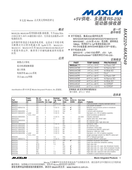

________________General DescriptionThe MAX3222/MAX3232/MAX3237/MAX3241 trans-ceivers have a proprietary low-dropout transmitter out-put stage enabling true RS-232 performance from a 3.0V to 5.5V supply with a dual charge pump. The devices require only four small 0.1µF external charge-pump capacitors. The MAX3222, MAX3232, and MAX3241 are guaranteed to run at data rates of 120kbps while maintaining RS-232 output levels. The MAX3237 is guaranteed to run at data rates of 250kbps in the normal operating mode and 1Mbps in the MegaBaud™ operating mode, while maintaining RS-232output levels.The MAX3222/MAX3232 have 2 receivers and 2 drivers. The MAX3222 features a 1µA shutdown mode that reduces power consumption and extends battery life in portable systems. Its receivers remain active in shutdown mode, allowing external devices such as modems to be monitored using only 1µA supply cur-rent. The MAX3222 and MAX3232 are pin, package,and functionally compatible with the industry-standard MAX242 and MAX232, respectively.The MAX3241 is a complete serial port (3 drivers/5 receivers) designed for notebook and subnotebook computers. The MAX3237 (5 drivers/3 receivers) is ideal for fast modem applications. Both these devices feature a shutdown mode in which all receivers can remain active while using only 1µA supply current. Receivers R1(MAX3237/MAX3241) and R2 (MAX3241) have extra out-puts in addition to their standard outputs. These extra outputs are always active, allowing external devices such as a modem to be monitored without forward bias-ing the protection diodes in circuitry that may have V CC completely removed.The MAX3222, MAX3237, and MAX3241 are available in space-saving TSSOP and SSOP packages.________________________ApplicationsNotebook, Subnotebook, and Palmtop Computers High-Speed Modems Battery-Powered Equipment Hand-Held Equipment Peripherals Printers__Next Generation Device Features♦For Smaller Packaging:MAX3228E/MAX3229E: +2.5V to +5.5V RS-232Transceivers in UCSP™♦For Integrated ESD Protection:MAX3222E/MAX3232E/MAX3237E/MAX3241E*/MAX3246E: ±15kV ESD-Protected, Down to 10nA,3.0V to 5.5V, Up to 1Mbps, True RS-232Transceivers♦For Low-Voltage or Data Cable Applications:MAX3380E/MAX3381E: +2.35V to +5.5V, 1µA, 2 Tx/2 Rx RS-232 Transceivers with ±15kV ESD-Protected I/O and Logic PinsMAX3222/MAX3232/MAX3237/MAX3241*3.0V to 5.5V , Low-Power , up to 1Mbps, T rue RS-232Transceivers Using Four 0.1µF External Capacitors________________________________________________________________Maxim Integrated Products119-0273; Rev 7; 1/07*Covered by U.S. Patent numbers 4,636,930; 4,679,134; 4,777,577; 4,797,899; 4,809,152; 4,897,774; 4,999,761; and other patents pending.Typical Operating Circuits appear at end of data sheet.Ordering Information continued at end of data sheet.For pricing, delivery, and ordering information,please contact Maxim/Dallas Direct!at 1-888-629-4642, or visit Maxim’s website at .+Denotes lead-free package.M A X 3222/M A X 3232/M A X 3237/M A X 3241Transceivers Using Four 0.1µF External Capacitors2_______________________________________________________________________________________ABSOLUTE MAXIMUM RATINGSELECTRICAL CHARACTERISTICS(V CC = +3.0V to +5.5V, C1–C4 = 0.1µF (Note 2), T A = T MIN to T MAX , unless otherwise noted. Typical values are at T A = +25°C.)Stresses beyond those listed under “Absolute Maximum Ratings” may cause permanent damage to the device. These are stress ratings only, and functional operation of the device at these or any other conditions beyond those indicated in the operational sections of the specifications is not implied. Exposure to absolute maximum rating conditions for extended periods may affect device reliability.Note 1:V+ and V- can have a maximum magnitude of 7V, but their absolute difference cannot exceed 13V.V CC ...........................................................................-0.3V to +6V V+ (Note 1)...............................................................-0.3V to +7V V- (Note 1)................................................................+0.3V to -7V V+ + V- (Note 1)...................................................................+13V Input VoltagesT_IN, SHDN , EN ...................................................-0.3V to +6V MBAUD...................................................-0.3V to (V CC + 0.3V)R_IN.................................................................................±25V Output VoltagesT_OUT...........................................................................±13.2V R_OUT....................................................-0.3V to (V CC + 0.3V)Short-Circuit DurationT_OUT....................................................................ContinuousContinuous Power Dissipation (T A = +70°C)16-Pin TSSOP (derate 6.7mW/°C above +70°C).............533mW 16-Pin Narrow SO (derate 8.70mW/°C above +70°C)....696mW 16-Pin Wide SO (derate 9.52mW/°C above +70°C)........762mW 16-Pin Plastic DIP (derate 10.53mW/°C above +70°C)...842mW 18-Pin SO (derate 9.52mW/°C above +70°C)..............762mW 18-Pin Plastic DIP (derate 11.11mW/°C above +70°C)..889mW 20-Pin SSOP (derate 7.00mW/°C above +70°C).........559mW 20-Pin TSSOP (derate 8.0mW/°C above +70°C).............640mW 28-Pin TSSOP (derate 8.7mW/°C above +70°C).............696mW 28-Pin SSOP (derate 9.52mW/°C above +70°C).........762mW 28-Pin SO (derate 12.50mW/°C above +70°C).....................1W Operating Temperature RangesMAX32_ _C_ _.....................................................0°C to +70°C MAX32_ _E_ _ .................................................-40°C to +85°C Storage Temperature Range.............................-65°C to +150°C Lead Temperature (soldering, 10s).................................+300°CMAX3222/MAX3232/MAX3237/MAX3241Transceivers Using Four 0.1µF External Capacitors_______________________________________________________________________________________3TIMING CHARACTERISTICS—MAX3222/MAX3232/MAX3241(V CC = +3.0V to +5.5V, C1–C4 = 0.1µF (Note 2), T A = T MIN to T MAX , unless otherwise noted. Typical values are at T A = +25°C.)ELECTRICAL CHARACTERISTICS (continued)(V CC = +3.0V to +5.5V, C1–C4 = 0.1µF (Note 2), T A = T MIN to T MAX , unless otherwise noted. Typical values are at T A = +25°C.)M A X 3222/M A X 3232/M A X 3237/M A X 3241Transceivers Using Four 0.1µF External Capacitors4_________________________________________________________________________________________________________________________________Typical Operating Characteristics(V CC = +3.3V, 235kbps data rate, 0.1µF capacitors, all transmitters loaded with 3k Ω, T A = +25°C, unless otherwise noted.)-6-5-4-3-2-101234560MAX3222/MAX3232TRANSMITTER OUTPUT VOLTAGEvs. LOAD CAPACITANCELOAD CAPACITANCE (pF)T R A N S M I T T E R O U T P U T V O L T A G E (V )20003000100040005000246810121416182022150MAX3222/MAX3232SLEW RATEvs. LOAD CAPACITANCELOAD CAPACITANCE (pF)S L E W R A T E (V /µs )20003000100040005000510152025303540MAX3222/MAX3232SUPPLY CURRENT vs. LOAD CAPACITANCEWHEN TRANSMITTING DATALOAD CAPACITANCE (pF)S U P P L Y C U R R E N T (m A )20003000100040005000TIMING CHARACTERISTICS—MAX3237(V CC = +3.0V to +5.5V, C1–C4 = 0.1µF (Note 2), T A = T MIN to T MAX , unless otherwise noted. Typical values are at T A = +25°C.)Note 2:MAX3222/MAX3232/MAX3241: C1–C4 = 0.1µF tested at 3.3V ±10%; C1 = 0.047µF, C2–C4 = 0.33µF tested at 5.0V ±10%.MAX3237: C1–C4 = 0.1µF tested at 3.3V ±5%; C1–C4 = 0.22µF tested at 3.3V ±10%; C1 = 0.047µF, C2–C4 = 0.33µF tested at 5.0V ±10%.Note 3:Transmitter input hysteresis is typically 250mV.MAX3222/MAX3232/MAX3237/MAX3241Transceivers Using Four 0.1µF External Capacitors_______________________________________________________________________________________5-7.5-5.0-2.502.55.07.50MAX3241TRANSMITTER OUTPUT VOLTAGEvs. LOAD CAPACITANCELOAD CAPACITANCE (pF)T R A N S M I T T E R O U T P U T V O L T A G E (V )2000300010004000500046810121416182022240MAX3241SLEW RATEvs. LOAD CAPACITANCELOAD CAPACITANCE (pF)S L E W R A T E (V /µs )20003000100040005000510152025303545400MAX3241SUPPLY CURRENT vs. LOADCAPACITANCE WHEN TRANSMITTING DATALOAD CAPACITANCE (pF)S U P P L Y C U R R E N T (m A )20003000100040005000-7.5-5.0-2.502.55.07.50MAX3237TRANSMITTER OUTPUT VOLTAGE vs. LOAD CAPACITANCE (MBAUD = GND)LOAD CAPACITANCE (pF)T R A N S M I T T E R O U T P U T V O L T A G E (V )200030001000400050000102030504060700MAX3237SLEW RATE vs. LOAD CAPACITANCE(MBAUD = V CC )LOAD CAPACITANCE (pF)S L E W R A T E (V /µs )500100015002000-7.5-5.0-2.502.55.07.50MAX3237TRANSMITTER OUTPUT VOLTAGE vs. LOAD CAPACITANCE (MBAUD = V CC )LOAD CAPACITANCE (pF)T R A N S M I T T E R O U T P U T V O L T A G E (V )5001000150020001020304050600MAX3237SUPPLY CURRENT vs.LOAD CAPACITANCE (MBAUD = GND)LOAD CAPACITANCE (pF)S U P P L Y C U R R E N T (m A )200030001000400050000246810120MAX3237SLEW RATE vs. LOAD CAPACITANCE(MBAUD = GND)LOAD CAPACITANCE (pF)S L E W R A T E (V /µs )2000300010004000500010302040506070MAX3237SKEW vs. LOAD CAPACITANCE(t PLH - t PHL )LOAD CAPACITANCE (pF)1000150050020002500_____________________________Typical Operating Characteristics (continued)(V CC = +3.3V, 235kbps data rate, 0.1µF capacitors, all transmitters loaded with 3k Ω, T A = +25°C, unless otherwise noted.)M A X 3222/M A X 3232/M A X 3237/M A X 3241Transceivers Using Four 0.1µF External Capacitors6_____________________________________________________________________________________________________________________________________________________Pin DescriptionMAX3222/MAX3232/MAX3237/MAX3241Transceivers Using Four 0.1µF External Capacitors_______________________________________________________________________________________7_______________Detailed DescriptionDual Charge-Pump Voltage ConverterThe MAX3222/MAX3232/MAX3237/MAX3241’s internal power supply consists of a regulated dual charge pump that provides output voltages of +5.5V (doubling charge pump) and -5.5V (inverting charge pump), regardless of the input voltage (V CC ) over the 3.0V to 5.5V range. The charge pumps operate in a discontinuous mode; if the output voltages are less than 5.5V, the charge pumps are enabled, and if the output voltages exceed 5.5V, the charge pumps are disabled. Each charge pump requires a flying capacitor (C1, C2) and a reservoir capacitor (C3, C4) to generate the V+ and V- supplies.RS-232 TransmittersThe transmitters are inverting level translators that con-vert CMOS-logic levels to 5.0V EIA/TIA-232 levels.The MAX3222/MAX3232/MAX3241 transmitters guaran-tee a 120kbps data rate with worst-case loads of 3k Ωin parallel with 1000pF, providing compatibility with PC-to-PC communication software (such as LapLink™).Typically, these three devices can operate at data rates of 235kbps. Transmitters can be paralleled to drive multi-ple receivers or mice.The MAX3222/MAX3237/MAX3241’s output stage is turned off (high impedance) when the device is in shut-down mode. When the power is off, the MAX3222/MAX3232/MAX3237/MAX3241 permit the outputs to be driven up to ±12V.The transmitter inputs do not have pullup resistors.Connect unused inputs to GND or V CC .MAX3237 MegaBaud OperationIn normal operating mode (MBAUD = G ND), the MAX3237 transmitters guarantee a 250kbps data rate with worst-case loads of 3k Ωin parallel with 1000pF.This provides compatibility with PC-to-PC communica-tion software, such as Laplink.For higher speed serial communications, the MAX3237features MegaBaud operation. In MegaBaud operating mode (MBAUD = V CC ), the MAX3237 transmitters guar-antee a 1Mbps data rate with worst-case loads of 3k Ωin parallel with 250pF for 3.0V < V CC < 4.5V. For 5V ±10%operation, the MAX3237 transmitters guarantee a 1Mbps data rate into worst-case loads of 3k Ωin parallel with 1000pF.Figure 1. Slew-Rate Test CircuitsLapLink is a trademark of Traveling Software, Inc.M A X 3222/M A X 3232/M A X 3237/M A X 3241Transceivers Using Four 0.1µF External Capacitors8_______________________________________________________________________________________RS-232 ReceiversThe receivers convert RS-232 signals to CMOS-logic out-put levels. The MAX3222/MAX3237/MAX3241 receivers have inverting three-state outputs. In shutdown, the receivers can be active or inactive (Table 1).The complementary outputs on the MAX3237 (R1OUTB)and the MAX3241 (R1OUTB, R2OUTB) are always active,regardless of the state of EN or SHDN . This allows for Ring Indicator applications without forward biasing other devices connected to the receiver outputs. This is ideal for systems where V CC is set to 0V in shutdown to accommodate peripherals, such as UARTs (Figure 2).MAX3222/MAX3237/MAX3241Shutdown ModeSupply current falls to less than 1µA in shutdown mode (SHDN = low). When shut down, the device’s charge pumps are turned off, V+ is pulled down to V CC , V- is pulled to ground, and the transmitter outputs are dis-abled (high impedance). The time required to exit shut-down is typically 100µs, as shown in Figure 3. Connect SHDN to V CC if the shutdown mode is not used. SHDN has no effect on R_OUT or R_OUTB.MAX3222/MAX3237/MAX3241Enable ControlThe inverting receiver outputs (R_OUT) are put into a high-impedance state when EN is high. The complemen-tary outputs R1OUTB and R2OUTB are always active,regardless of the state of EN and SHDN (Table 1). EN has no effect on T_OUT.__________Applications InformationCapacitor SelectionThe capacitor type used for C1–C4 is not critical for proper operation; polarized or nonpolarized capacitors can be used. The charge pump requires 0.1µF capaci-tors for 3.3V operation. For other supply voltages, refer to Table 2 for required capacitor values. Do not use values lower than those listed in Table 2. Increasing the capaci-tor values (e.g., by a factor of 2) reduces ripple on the transmitter outputs and slightly reduces power consump-tion. C2, C3, and C4 can be increased without changing C1’s value. However, do not increase C1 without also increasing the values of C2, C3, and C4, to maintain the proper ratios (C1 to the other capacitors).When using the minimum required capacitor values,make sure the capacitor value does not degrade exces-sively with temperature. If in doubt, use capacitors with a higher nominal value. The capacitor’s equivalent series resistance (ESR), which usually rises at low tempera-tures, influences the amount of ripple on V+ and V-.Figure 2. Detection of RS-232 Activity when the UART and Interface are Shut Down; Comparison of MAX3237/MAX3241(b) with Previous Transceivers (a).MAX3222/MAX3232/MAX3237/MAX3241Transceivers Using Four 0.1µF External Capacitors_______________________________________________________________________________________9Power-Supply DecouplingIn most circumstances, a 0.1µF bypass capacitor is adequate. In applications that are sensitive to power-supply noise, decouple V CC to ground with a capacitor of the same value as charge-pump capacitor C1. Connect bypass capacitors as close to the IC as possible.Operation Down to 2.7VTransmitter outputs will meet EIA/TIA-562 levels of ±3.7V with supply voltages as low as 2.7V.Transmitter Outputs whenExiting ShutdownFigure 3 shows two transmitter outputs when exiting shutdown mode. As they become active, the two trans-mitter outputs are shown going to opposite RS-232 lev-els (one transmitter input is high, the other is low).Each transmitter is loaded with 3k Ωin parallel with 2500pF. The transmitter outputs display no ringing or undesirable transients as they come out of shutdown.Note that the transmitters are enabled only when the magnitude of V- exceeds approximately 3V.Mouse DriveabilityThe MAX3241 has been specifically designed to power serial mice while operating from low-voltage power sup-plies. It has been tested with leading mouse brands from manufacturers such as Microsoft and Logitech. The MAX3241 successfully drove all serial mice tested and met their respective current and voltage requirements.Figure 4a shows the transmitter output voltages under increasing load current at 3.0V. Figure 4b shows a typical mouse connection using the MAX3241.CC = 3.3V C1–C4 = 0.1µF50µs/divFigure 3. Transmitter Outputs when Exiting Shutdown or Powering UpM A X 3222/M A X 3232/M A X 3237/M A X 3241Transceivers Using Four 0.1µF External Capacitors10______________________________________________________________________________________Figure 4b. Mouse Driver Test Circuit Figure 4a. MAX3241 Transmitter Output Voltage vs. Load Current per TransmitterMAX3222/MAX3232/MAX3237/MAX3241Transceivers Using Four 0.1µF External Capacitors______________________________________________________________________________________11High Data RatesThe MAX3222/MAX3232/MAX3241 maintain the RS-232±5.0V minimum transmitter output voltage even at high data rates. Figure 5 shows a transmitter loopback test circuit. Figure 6 shows a loopback test result at 120kbps, and Figure 7 shows the same test at 235kbps.For Figure 6, all transmitters were driven simultaneously at 120kbps into RS-232 loads in parallel with 1000pF.For Figure 7, a single transmitter was driven at 235kbps,and all transmitters were loaded with an RS-232 receiver in parallel with 1000pF.The MAX3237 maintains the RS-232 ±5.0V minimum transmitter output voltage at data rates up to 1Mbps.Figure 8 shows a loopback test result at 1Mbps with MBAUD = V CC . For Figure 8, all transmitters were loaded with an RS-232 receiver in parallel with 250pF.CC = 3.3V5µs/divFigure 5. Loopback Test CircuitFigure 6. MAX3241 Loopback Test Result at 120kbpsCC = 3.3V2µs/divFigure 7. MAX3241 Loopback Test Result at 235kbps0V +5V 0V -5V +5V 0VT_INT_OUT = R_IN 5k R_OUT 150pF200ns/divCC = 3.3VFigure 8. MAX3237 Loopback Test Result at 1000kbps (MBAUD = V CC )M A X 3222/M A X 3232/M A X 3237/M A X 3241Transceivers Using Four 0.1µF External Capacitors__________________________________________________Typical Operating CircuitsInterconnection with 3V and 5V LogicThe MAX3222/MAX3232/MAX3237/MAX3241 can directly interface with various 5V logic families, includ-ing ACT and HCT CMOS. See Table 3 for more informa-tion on possible combinations of interconnections.Table 3. Logic-Family Compatibility with Various Supply VoltagesMAX3222/MAX3232/MAX3237/MAX3241Transceivers Using Four 0.1µF External Capacitors______________________________________________________________________________________13_____________________________________Typical Operating Circuits (continued)M A X 3222/M A X 3232/M A X 3237/M A X 3241Transceivers Using Four 0.1µF External Capacitors14___________________________________________________________________________________________________________________________________Pin Configurations (continued)MAX3222/MAX3232/MAX3237/MAX3241Transceivers Using Four 0.1µF External Capacitors______________________________________________________________________________________15______3V-Powered EIA/TIA-232 and EIA/TIA-562 Transceivers from MaximOrdering Information (continued)*Dice are tested at T A = +25°C, DC parameters only.+Denotes lead-free package.M A X 3222/M A X 3232/M A X 3237/M A X 3241Transceivers Using Four 0.1µF External Capacitors16_________________________________________________________________________________________________________Chip Topography___________________Chip InformationT1INT2IN 0.127"(3.225mm)0.087"(2.209mm)R2OUTR2IN T2OUTV CCV+C1+SHDNENC1- C2+C2-V-MAX3222TRANSISTOR COUNT: 339SUBSTRATE CONNECTED TO GNDTransceivers Using Four 0.1µF External CapacitorsPackage Information (The package drawing(s) in this data sheet may not reflect the most current specifications. For the latest package outline information, go to /packages.)Revision HistoryPages changed at Rev 7: 1, 15, 16, 17Maxim cannot assume responsibility for use of any circuitry other than circuitry entirely embodied in a Maxim product. No circuit patent licenses are implied. Maxim reserves the right to change the circuitry and specifications without notice at any time.17__________________Maxim Integrated Products, 120 San Gabriel Drive, Sunnyvale, CA 94086 (408) 737-7600©2007 Maxim Integrated Products is a registered trademark of Maxim Integrated Products, Inc.。

DATA SHEET OPTIV CLASSIC 322PRODUCT DESCRIPTIONThe Optiv Classic 322 combines optical and tactile measurement in one system (optional touch-trigger probe).The system supports multi-sensor measurements using the Vision sensor (CMOS colour camera, motorised CNC zoom) and the touch-trigger probe HP-TM. The Optiv Classic 322 provides easy pallet station integration with good accessibility to the measuring table from all sides. Measurement software is PC-DMIS.FIELDS OF APPLICATION• Shop floor and inspection room• Versatile geometry measurements and GD&T analysisDESIGNDesign principle : Benchtop unit of proven cross-table design with a solid metal base frame as a standardGuides : Mechanical linear guides on all axes, counterbalance on Z axisDrives : DC servo motors, power transmission via plain shafts in conjunction with rolling ring drivesLength measuring system : Incremental, optoelectronic length measuring systemResolution of the scales : 0.05 µmMEASURING RANGE (X x Y x Z)OPTIV CLASSIC 322X300 mm (11.5 in.)256 mm (10 in.)256 mm (10 in.)Y200 mm (7.5 in.)175 mm (6.5 in.)175 mm (6.5 in.)Z200 mm (7.5 in.)(2)200 mm (7.5 in.)(2)200 mm (7.5 in.)(2)(1) Vision sensor <—> Touch-trigger probe, see page 6. (2) At a maximum workpiece depth in Y of 140 mm, otherwise Z = 80 mm.LOADING CAPACITY• Load-bearing capacity of the table up to 16 kgDIMENSIONS IN MM AND WEIGHTS IN KG• Dimensions see machine layout on page 5• Machine weight 260 kg + base frame 45 kgMEASURING ACCURACY(3)XY measuring accuracy MPE (Exy) = (2.8 + L/150) µm XY measuring accuracy MPE (Exy) = (2.8 + L/150) µmZ measuring accuracy MPE (Ez) = (5.0 + L/150) µm Z measuring accuracy MPE (Ez) = (5.0 + L/150) µm(3) The conditions of acceptance of Hexagon Metrology Vision apply. L = measurement length in mm.HEXAGON MANUFACTURING INTELLIGENCE | 2OPTIV CLASSIC 322 AIRBORNE NOISE EMISSIONS• The A-weighted emission sound pressure level at operator’s position is less than 70 db(A). ENVIRONMENTAL REQUIREMENTS• Air humidity 45 % - 75 % RL, non-condensing• Environmental temperature 20 °C ± 2 °C• Permissible temperature gradient 1.0 °C/h, 2.0 °C/d, 1.0 °C/m• Max. installation height 2000 m above sea levelTHROUGHPUT• Max. traversing speed : X, Y = 165 mm/s, Z = 60 mm/sVISION SENSORTechnical description :• Sensor for non-contact measurement of smallest and closely toleranced features- H igh resolution digital 1/1.8-inch CMOS colour camera with Gigabit Ethernet interface, for interference-free,low noise image reproduction- Maximum optical precision due to low distortion optics : Motorised CNC zoom- Powerful image processing> Fast, precision video autofocus> Automatic feature detection, geometry and bad pixel video filters> C ontour scanning mode : Sophisticated set of user-selectable algorithms to setup edge detection,intelligent, automatic selection of the most suitable setting for the measurement> Best fit routines> A utoTune : Transferability of measuring programs between machines of the same type> M ultiCapture : MultiCapture allows all 2D features within a field of view to be captured simultaneously,regardless of the feature type. Inspection speeds can be increased by 35 % or more, depending on the featuresize and density. The capture sequence for groups of features using MultiCapture is also automaticallyoptimised, creating the most efficient possible path with the fewest number of stage movements.> R GB Sensitivity Adjustments for colour cameras : Software controls for Red/Green/Blue (RGB) sensitivity inimages from a colour camera allow for fine control adjustment over image contrast. This capability improvesoverall consistency in vision inspection in general and is especially useful for coloured parts where edges can bedifficult to capture with grayscale or lighting modifications alone.Illumination for Vision sensor :• Coaxial LED top light• LED back light• Multi-segment LED ring light : 4 quadrants• Laserpointer (simplifies navigation during the measuring program generation)CNC zoom :• M otorised zoom, for a continuous adjustment of field of view and resolution : Standard: 6.5x• H igh resolution digital 1/1.8-inch CMOS colour camera (H 1280 x V 1024) with Gigabit Ethernet interface MAGNIFICATION VARIANTS OF THE 6.5X CNC ZOOM(1)Standard0.74x to 4.4x920 to 1309.2 x 7.3 1.53 x 1.227.2 bis 1.249x to 295x(1) Values rounded. (2) Optical. (3) Without multi-segment LED ring light (When using a multi-segment LED ring light, these values are reduced by the amount of the overall heightof the ring light (approx. 30 mm).). (4) On a 22-inch (16:9) monitor, PC-DMIS “Scale to Fit” —> OFF. | HEXAGON MANUFACTURING INTELLIGENCE3TOUCH-TRIGGER PROBE HP-TM (OPTIONAL)• T he5-way touch-trigger probe consistsof the sensor body and the stylus holding module that are magnetically connected to each other.• T he stylus holding modules are available in four versions with different trigger forces.±X, ±Y, +Z M8 thread(probe body),M2 thread(styli)Four :• L Flow force• S Fstandardforce• M Fmediumforce• E Fextendedforce0.35 µm(LF module),0.35 µm(SF module),0.50 µm(MF module),0.65 µm(EF module)± 0.60 µm(LF module),± 0.80 µm(SF module),± 1.00 µm(MF module),± 2.00 µm(EF module)0.055 N,L = 10 mm(LF module),0.08 N,L = 10 mm(SF module),0.10 N,L = 25 mm(MF module),0.10 N,L = 50 mm(EF module)X/Y = +/- 16°,Z = + 5 mmHR-P with4 slotsMutual measuring range Vision sensor <—> Touch-trigger probe, see page 6.CONTROL SYSTEM AND SAFETY REGULATIONS• Machine control unit : DELL computer system with Microsoft Windows 10 Professional (64 bit)• CNC controller : Microprocessor CNC with vector path control• S afety equipment:- E mergency-Stop circuit with Emergency-Stop button- A xis drive via rolling ring drive with safety slip clutch- S cale signal monitoring- P rotective covers for the axes’ drives- C ollision protection for touch-trigger probes• S afety regulations:- D IN EN ISO 12100-1 and -2 (Safety of machinery)- DIN EN 60204-1 (Safety of machinery - Electrical equipment of machines)- DIN EN ISO 13849-1 (Safety of machinery - Safety-related parts of control systems)- D IN EN 61000-4-2 and -4 (Electromagnetic compatibility EMC, immunity of machines)- D IN EN 55011 (Industrial, scientific and medical equipment - Radio-frequency disturbance characteristics) SUPPLY DATA• I nput voltage power supply 115-230 V ± 10%• F requency 50/60 Hz ± 5%• P ower consumption (max.) 690 WOPTIONAL EQUIPMENT• T ouch-trigger probe HP-TM• S tylus module changing rack HR-P with 4 slots• R otary indexing table• P eriphery:- W orktable- P rinters,monitorsHEXAGON MANUFACTURING INTELLIGENCE | 4OPTIV CLASSIC 322 MACHINE LAYOUT | HEXAGON MANUFACTURING INTELLIGENCE5HEXAGON MANUFACTURING INTELLIGENCE | 6STAGE LAYOUTOPTIV CLASSIC 322 ROTARY INDEXING TABLE (OPTIONAL)ROTARY INDEXING TABLE FOROPTIV CLASSIC 322, 432, 443 ANDOPTIV PERFORMANCE 322In this separate data sheet, you will findfurther information on the optionally availablerotary indexing table. | HEXAGON MANUFACTURING INTELLIGENCE7Hexagon Manufacturing Intelligence helps industrial manufacturers develop the disruptive technologies of today and the life-changing products of tomorrow. As a leading metrology and manufacturing solution specialist, our expertise in sensing, thinking and acting – the collection, analysis and active use of measurement data – gives our customers the confidence to increase production speed and accelerate productivity while enhancing product quality. Through a network of local service centres, production facilities and commercial operations across five continents, we are shaping smart change in manufacturing to builda world where quality drives productivity. For more information, visit .Hexagon Manufacturing Intelligence is part of Hexagon (Nasdaq Stockholm: HEXA B; ), a leading global provider of information technologies that drive quality and productivity across geospatial and industrial enterprise applications.COORDINATE MEASURING MACHINES 3D LASER SCANNINGSENSORSPORTABLE MEASURING ARMS SERVICESLASER TRACKERS & STATIONS MULTISENSOR & OPTICAL SYSTEMS WHITE LIGHT SCANNERS METROLOGY SOFTWARE SOLUTIONS CAD / CAMSTATISTICAL PROCESS CONTROL AUTOMATED APPLICATIONS MICROMETERS, CALIPERS AND GAUGES DESIGN AND COSTING SOFTWARE© 2018 Hexagon AB and / or its subsidiaries and affiliates. All rights reserved. This document is accurate as of its publication date. Information is subject to change without notice.。

1S E M I C O N D U C T O R SSUMMARYNPN —-V CEO = 80V; R SAT =68m ; I C = 3.5A DESCRIPTIONPackaged in the new innovative 2mm x 2mm MLP (Micro Leaded Package)outline,these new 4th generation low saturation dual PNP transistors offer extremely low on state losses making them ideal for use in DC-DC circuits and various driving and power management functions.Additionally users gain several other key benefits :Performance capability equivalent to much larger packages Improved circuit efficiency & power levels PCB area and device placement savings Lower Package Height (0.9mm nom)Reduced component countFEATURES•Low Equivalent On Resistance•Extremely Low Saturation Voltage (185mV max @1A)•h FE specified up to 5A•I C =-3.5A Continuous Collector Current •2mm x 2mm MLPAPPLICATIONS•DC - DC Converters •DC - DC Modules •Power switches •Motor controlDEVICE MARKING•SEZXTEM322ISSUE 1 - JUNE 2003MPPS TM Miniature Package Power Solutions 80V NPN LOW SATURATION TRANSISTORDEVICE REEL SIZE TAPE WIDTH QUANTITY PER REELZXTEM322TA 7”8mm 3000ZXTEM322TC13”8mm10000ORDERING INFORMATIONMLP322ZXTEM322S E M I C O N D U C T O R SISSUE 1 - JUNE 20032PARAMETERSYMBOL VALUE UNIT Junction to Ambient (a)R ⍜JA 83ЊC/W Junction to Ambient (b)R ⍜JA 51ЊC/W Junction to Ambient (d)R ⍜JA 125ЊC/W Junction to Ambient (e)R ⍜JA42ЊC/WNOTES(a)For a single device surface mounted on 10sq cm 1oz copper on FR4 PCB, in still air conditions with all exposed pads attached .(b) For a single device surface mounted on 10sq cm 1oz copper on FR4 PCB, in still air conditions measured at t Յ5 secs with all exposed pads attached .(c) Repetitive rating - pulse width limited by max junction temperature. Refer to Transient Thermal Impedance graph.(d) For a single device surface mounted on 10 sq cm 1oz copper FR4 PCB, in still air conditions with minimal lead connections only.(e) For a single device surface mounted on 65 sq cm 2oz copper FR4 PCB, in still air conditions with all exposed pads attached .(f) The minimum copper dimensions required for mounting are no smaller than the exposed metal pads on the base of the device, as shown in the package dimensions data. The thermal resistance for a device mounted on 1.5mm thick FR4 board using minimum copper of 1oz weight and 1mm wide tracks is Rth= 300°C/W giving a power rating of Ptot=420mWTHERMAL RESISTANCEPARAMETERSYMBOL LIMIT UNIT Collector-Base Voltage V CBO 100V Collector-Emitter Voltage V CEO 80V Emitter-Base Voltage V EBO 7.5V Peak Pulse CurrentI CM 5A Continuous Collector Current (a)I C 3.5A Base CurrentI B 1000mA Power Dissipation at TA=25°C (a)Linear Derating FactorP D 1.512W mW/ЊC Power Dissipation at TA=25°C (b)Linear Derating FactorP D 2.4519.6W mW/ЊC Power Dissipation at TA=25°C (d)Linear Derating FactorP D 18W mW/ЊC Power Dissipation at TA=25°C (e)Linear Derating FactorP D 324W mW/ЊC Operating &Storage Temperature Range T j :T stg -55 to +150ЊC Junction TemperatureT j150ЊCABSOLUTE MAXIMUM RATINGSZXTEM322S E M I C O N D U C T O R SISSUE 1 - JUNE 20033ZXTEM322S E M I C O N D U C T O R SISSUE 1 - JUNE 2003 4PARAMETER SYMBOL MIN.TYP.MAX.UNIT CONDITIONS Collector-Base Breakdown Voltage V(BR)CBO100180V I C=100A Collector-Emitter Breakdown Voltage V(BR)CEO80110V I C=10mA* Emitter-Base Breakdown Voltage V(BR)EBO7.58.2V I E=100A Collector Cut-Off Current I CBO25nA V CB=80V Emitter Cut-Off Current I EBO25nA V EB=6V Collector Emitter Cut-Off Current I CES25nA V CE=65VCollector-Emitter Saturation Voltage V CE(sat)15451451602402060185200325mVmVmVmVmVI C=0.1A,I B=10mA*I C=0.5A,I B=50mA*I C=1A,I B=20mA*I C=1.5A,I B=50mA*I C=3.5A,I B=300mA*Base-Emitter Saturation Voltage V BE(sat) 1.09 1.175V I C=3.5A,I B=300mA* Base-Emitter Turn-On Voltage V BE(on)0.96 1.05V I C=3.5A,V CE=2V*Static Forward Current Transfer Ratio h FE2003001106020450450170903010900I C=10mA,V CE=2V*I C=200mA,V CE=2V*I C=1A,V CE=2V*I C=1.5A,V CE=2V*I C=3A,V CE=2V*I C=5A,V CE=2V*Transition Frequency f T100160MHz I C=50mA,V CE=10Vf=100MHzOutput Capacitance C obo11.518pF V CB=10A,f=1MHzTurn-On Time t(on)86ns VCC =10V,I C=1AI B1=I B2=25mA Turn-Off Time t(off)1128ns ELECTRICAL CHARACTERISTICS(at T amb= 25°C unless otherwise stated)*Measured under pulsed conditions. Pulse width=300s. Duty cycleՅ2%ZXTEM322S E M I C O N D U C T O R SISSUE 1 - JUNE 20035ZXTEM322S E M I C O N D U C T O R S6ISSUE 1 - JUNE 2003EuropeZetex plcFields New Road ChaddertonOldham, OL9 8NP United KingdomTelephone (44) 161 622 4444Fax: (44) 161 622 4446hq@Zetex GmbHStreitfeldstraße 19D-81673 München GermanyTelefon: (49) 89 45 49 49 0Fax: (49) 89 45 49 49 49europe.sales@AmericasZetex Inc700 Veterans Memorial Hwy Hauppauge, NY 11788USATelephone: (1) 631 360 2222Fax: (1) 631 360 8222usa.sales@Asia PacificZetex (Asia) Ltd3701-04Metroplaza Tower 1Hing Fong Road Kwai Fong Hong KongTelephone: (852) 26100 611Fax: (852) 24250 494asia.sales@These offices are supported by agents and distributors in major countries world-wide.This publication is issued to provide outline information only which (unless agreed by the Company in writing)may not be used,applied or reproduced for any purpose or form part of any order or contract or be regarded as a representation relating to the products or services concerned.The Company reserves the right to alter without notice the specification,design,price or conditions of supply of any product or service.For the latest product information,log on to©Zetex plc 2003DIM Millimetres Inches DIM Millimetres Inches Min Max Min Max MinMaxMinMaxA 0.80 1.000.03150.0393e 0.65 REF 0.0255 REF A10.000.050.000.002E 2.00 BSC 0.0787 BSC A20.650.750.02550.0295E20.790.990.0310.039A30.150.250.00590.0098E40.480.680.01880.0267b 0.180.280.00700.0110L 0.200.450.00780.0177b10.170.300.00660.0118L20.125 MAX.0.005 REF D 2.00 BSC 0.0787 BSCr 0.075 BSC 0.0029 BSC D2 1.22 1.420.04800.0559⍜0Њ12Њ0Њ12ЊD40.560.760.02200.0299PACKAGE DIMENSIONSControlling dimensions are in millimetres. Approximate conversions are given in inches。