CM400DU-24NFH中文资料
- 格式:pdf
- 大小:57.90 KB
- 文档页数:4


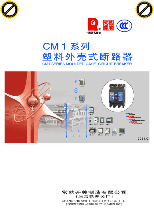
CM 1系列塑料外壳式断路器CM1SERIES MOULDED CASE CIRCUIT BREAKER常熟开关制造有限公司(原常熟开关厂)CHANGSHU SWITCHGEAR MFG.CO.,LTD.(FORMER CHANGSHU SWITC HGEAR PLANT )CV 系列CW 系列CM 系列CK 系列CR 系列CA 系列CJR 系列CJD 系列CD 系列CH 系列CE 系列CB 系列S2011.03适用范围………………………………适用工作环境…………………………断路器的分类…………………………CM1快速选用表……………………脱扣器方式及内部附件代号…………四极断路器规格………………………保护特性………………………………功耗及降容系数………………………高海拔降容…………………………断路器特性曲线………………………断路器主要技术性能指标………………………………..........................................外形尺寸及安装尺寸............断路器安装安全间隙内外部附件........................接线端子型号........................FWB1温度报警模块使用与维护...........................订货须知..............................限流特性.................................订货规范 (1123456778111937)385152535555565759消防用过载不脱扣只报警接线参考图……不同额定电流的连接导线参考截面Application range ………………………………Applicable environment condition ………………Classification of CM1circuit breakers …………Table for choosing quickly the CM1series ………Release pattern and accessories code ……………Specification of four-poles breaker ………………Protection feature ………………………………Power wastage and capacity-reducing factor ……Capacity-reducing for high-elevation …………Characteristic curve ……………………………Main technical-performance index ……………Outline dimensions and mounting dimensions …Mounting safety clearance ………………………Internal/external accessories ……………………Type of wiring terminal …………………………Temperature alarm module ………………………Use and maintenance …………………………Ordering notice ………………………………Limited characteristic …………………………Ordering form ………………………………………Cross-section areaof wiring cable and corresponding rated current 1123456778111937385152535555565759Wiring referential diagram of fire control without release but alarm due to overload ………………CM1系列塑料外壳式断路器(以下简称断路器),是本公司采用国际先进设计、制造技术研制、开发的新型断路器之一。


功率器件损耗计算于两个方面:器件内部和器件外部。
器件工作时所耗散的功率要通过发热形式耗散出去。
若器件的散热能力有限,则功率的耗散就会造成器件内部芯片有源区温度上升及结温升高,使得器件可靠性降低,无法安全正常工作。
在实际应用中,为了保证某些重要功率器件,在这些器件上使用散热器来控制其的工作温升。
功率器件常用的散热方式是使用散热器。
散热器设计的选用主要依靠功率器件的损耗发热量。
在计算出损耗量的前提下,对散热器的各个参数进行设计。
在开关电源系统中功率器件有7 个IGBT 和2 个整流桥,其损耗量计算如下:IGBT 的散热器有两组:其中U1、U2、U3 为一组,U4、U5、U6、U7 为一组。
U1、U2、U3 损耗:流过电流Io=228A工作电压Vcc=620V工作频率fc=3kHZ其它计算参数由CM600DU-24NFH 提供的参数表查得;通过CM600DU-24NFH 自带损耗计算软件可算得一个IGBT 模块的损耗量,如下图:由计算结果可知:P1=389.51WPo=3 乘以P1=3 乘以389.51=1168.53WU4、U5、U6、U7 损耗:流过电流Io=114A工作电压Vcc=620V工作频率fc=20kHZ其它计算参数由CM600DU-24NFH 提供的参数表查得;通过CM600DU-24NFH 自带损耗计算软件可算得一个IGBT 模块的损耗量,如下图:由计算结果可知:P1=476.82WPo=4 乘以P1=4 乘以476.82=1907.28W整流桥D1、D2 损耗计算整流桥是由四个二极管构成,主要的损耗来自二极管PN 结。
二极管的损耗包括正向导通损耗、反向恢复损耗和断态损耗。
肖特级二极管的反向时间很短,反向损耗可以忽略不计。
一般来说,二极管的截止损耗在总功耗中所占的比例很小,可以忽略不计。
在实际应用中,只考虑其的正向导通损耗。
二极管的正向导通损耗可由下式求出:v L@--防复制原创安全保护系统a),S #$`Pdiode.F=VFIFd@_bo]Kpqq]--cn-pereMHUhp|=式中VF DD 二极管正向导通压降; ujOn?€}4--防复制原创安全保护系统w Yu5 4I+IF DD 二极管的正向导通电流; |W+)w F--未经许可,禁止转载Hinwl N])dDD 二极管工作的占空比根据查SKKE 310F 参数可知:VF = 2.1 V IF=400 A d = 0.25由此可得单个二极管的损耗Pdiode.FPdiode.F=VFIFd=2.1V 乘以400A 乘以0.25=210W整流桥中的四个上二极管是交替工作的,每次工作是只有两个,所以整流桥的损耗为二极管的两倍,则:P=2 乘以Po=2 乘以210W=420W整个开关电源系统中共有两个整流桥同时工作,它们共有一个散热器进行散热。

5. 生产基板的变更在与上次不同的基板上实装元件时,需要调整与基板相对应的装置及进行生产材料的供给。
在本章中把生产基板的数据作为PT侧的数据说明了生产基板的变更的操作。
5.1 随生产基板变更的机器位置调整部位5.2 生产数据的变更5.2 生产数据的变更1235.3 搬送导轨宽度的调整下一页5.3 搬送导轨宽度的调整4Z4C-CEn-Ma-0011 4Z4C-CEn-MaCa-0024Z4C-CEn-Ma-0015.4 支撑销的安装4Z4C-CEn-Pc-001SERVOOFF ( )ON ( )下一页5.4 支撑销的安装444C-107P444C-108P444C-107P下一页5.4 支撑销的安装14Z4C-CEn-PcSp-0025.5 吸嘴的交换5.5 吸嘴的交换5.5 吸嘴的交换4Z4C-CEn-Pc-0011SERVOOFF ( )ON ( )5.5 吸嘴的交换5.5 吸嘴的交换4Z4C-CEn-Pc-001SERVOOFF ( )ON ( )5.5 吸嘴的交换5.6 生产材料的配置及确认4Z4C-CEn-DmFl-0015.7 基板搬送测试4Z4C-CEn-Main-001下一页5.7 基板搬送测试5.8 根据条件实装确认实装状态下一页5.8 根据条件实装确认实装状态1 在步骤3.中按下[部品]时12在步骤3.中按下[区块]时1CM402操作手册5.8 根据条件实装确认实装状态Page 5-21下一页4Z4C-C-OMA05-A01-00 4Z4C-CEn-PrCm-001CM402操作手册5.8 根据条件实装确认实装状态4Z4C-CEn-PrCs-002Page 5-22 4Z4C-C-OMA05-A01-00。

Appendix KPreparing and activating a replacement CM 4000As discussed on page 2−8, CM 4000s can be installed as a redundant pair, so that failure of one unit will result in control being taken by the second. A third unit can be kept in reserve and, in the event of a failure, have its address altered and be installed to provide a quick replacement for the failed unit and restore system redundancy. See Figure K−1.Replacement CM 4000REPLACING A FAILED UNITA fault condition should be indicated by a “00,” “01,” or “FF” indication on the front panel LED display, or, in the case of a failed power supply, no lamps illuminated. Control should have switched to the other CM by this point. Check that it has by looking for the green Activate lamp. Then proceed as follows:1.If necessary, switch control manually to the good unit by pressing the Activate button.Figure K −2.button 2.De −power the faulty CM 4000.3.Before installing the replacement unit, change its physical Ethernet address (MAC address) to match that of the failedCM 4000:Caution: Changing the physical address of the CM 4000 can have undesirable results if not done properly. Itis very important to maintain strict control of the addresses of all units in and out of the system to avoid net-work conflicts.The physical Ethernet address is stored in a serial EEPROM chip. The data in this chip is validated with twochecksums. If either checksum is invalid, the Ethernet chip will fail to initialize and will not function. Be-cause of this, it is very important that during the EEPROM write procedure, the CM 4000 is not reset or powerinterrupted until the write cycle is completed.a.On the replacement CM, connect a terminal to the front console port and power up the unit. It is stressed that thisprocedure is done with the replacement CM 4000 out of the system where there can be no address conflict .b.Stop the boot process at the ‘Press any key to stop auto −boot.’ prompt.Press any key to stop auto −boot (1)c.At the VxWorks boot prompt, enter ‘N’ and then press ‘enter’.[VxWorks Boot]: N[ENTER]d.Wait for the EEPROM memory to get read:Reading EEPROM ..................................Replacement CM 4000The current Ethernet address will be displayed:Current Ethernet Address is: 00:40:53:12:34:56The first 3 bytes of the Ethernet address are the manufacturer’s ID and cannot be changed. The fourth byte will be shown with an option to change it:00− 0040− 4053− 5312− _e.Modify the last 3 bytes to match those of the failed CM 4000.Enter the new digits and press Enter to change Byte 4 or press Enter alone to keep the current byte. In this example, the 4th byte is changed to “21.”12− 21[ENTER]Repeat the process for the remaining two bytes. In this example, the 5th byte will be kept the same, and the 6th byte changed to ”65”:34− [ENTER]56− 65[ENTER]f.The EEPROM will now be re−written. During this time, do not reset the CM 4000 or allow the power to reset.Writing EEPROM .....When the write cycle is complete, the new current Ethernet address will be displayed with the vxWorks prompt:New Ethernet Address is: 00:40:53:21:34:65[VxWorks Boot]:Make a note of this number (e.g., by writing it on the CM back panel).g.Remove power from the CM 4000.4.Make sure that power has been removed from the faulty CM 4000, then disconnect it from the system while noting cablepositions.5.Install, connect, and power up the replacement CM 4000.The replacement CM 4000 will boot up automatically. The other CM 4000 should remain active throughout this opera-tion.6.Confirm that the system is still operating normally by using a Jupiter control panel.Ensure that the status of all crosspoints on the switcher is reported on the panel.Replacement CM 40007.To verify that the replacement unit is ready for use:a.Go to “JNS Applications > Control Center > Bootp” and check that the correct MAC address is being used for thereplacement CM. Also go to the “TFTP Status” tab and look for an indication that the “transfer succeeded” (“100% complete”). If these indications are correct, proceed as follows:b.Swap control to the replacement CM 4000 by pressing the Activate button.c.Confirm system operation.d.Assuming all is well leave the replacement CM 4000 in control of the system. The installation is now complete.Should problems be experienced return control immediately to the opposite CM 4000. De−power the replacement CM 4000, check all cabling, and reapply power. Should this fail to eliminate the fault, it may be necessary to download a new configura-tion set; refer to “Validating, Compiling, and Activating (Downloading) a Configuration Set” on page 5−13.If problems persist, contact Thomson Technical Support.。

V CE = V CES , V GE = 0V V GE = V GES , V CE = 0V T j = 25°CT j = 125°C V CC = 600V, I C = 300A, V GE = 15VV CC = 600V, I C = 300A V GE1 = V GE2 = 15VR G = 1.0Ω, Inductive load switching operation I E = 300AI E = 300A, V GE = 0V IGBT part (1/2 module)*1FWDi part (1/2 module)*1Case to fin, Thermal compound Applied (1/2 module)*1,*2I C = 30mA, V CE = 10VI C = 300A, V GE = 15VV CE = 10V V GE = 0V1200±203006003006001890–40 ~ +150–40 ~ +12525003.5 ~ 4.53.5 ~ 4.5400HIGH POWER SWITCHING USEV V A A W °C °C V N • m g10.53.0—4740.9—550180600350250—3.80.0660.12—16mA µA nF nC ns µC V °C/W Ω——2.12.4———1350—————9.0———0.02———————————————————1.07V V 68ns I CES I GES C ies C oes C res Q G t d(on)t rt d(off)t ft rr (Note 1)Q rr (Note 1)V EC(Note 1)R th(j-c)Q R th(j-c)R R th(c-f)R GSymbol ParameterV GE(th)V CE(sat)*1 : Tc, Tf measured point is just under the chips.*2 : Typical value is measured by using Shin-etsu Silicone “G-746”.Note 1. I E , V EC , t rr & Q rr represent characteristics of the anti-parallel, emitter to collector free-wheel diode (FWDi).2. Pulse width and repetition rate should be such that the device junction temp. (T j ) does not exceed T jmax rating.3. Junction temperature (T j ) should not increase beyond 150°C.Collector-emitter voltage Gate-emitter voltage Maximum collector dissipation Junction temperature Storage temperature Isolation voltage WeightG-E Short C-E ShortDC, T C = 80°C *1Pulse (Note 2)Pulse(Note 2)T C = 25°C *1Main terminal to base plate, AC 1 min.Main terminal M6Mounting holes M6Typical valueSymbol ParameterCollector current Emitter currentTorque strength ConditionsUnit Ratings V CES V GES I C I CMI E (Note 1)I EM (Note 1)P C (Note 3)T j T stg V iso———Unit Typ.Limits Min.Max.Test conditionsELECTRICAL CHARACTERISTICS (Tj = 25°C)ABSOLUTE MAXIMUM RATINGS (Tj = 25°C)Collector cutoff current Gate-emitter threshold voltageGate leakage currentCollector-emitter saturation voltageInput capacitance Output capacitanceReverse transfer capacitance Total gate charge Turn-on delay time Turn-on rise time Turn-off delay time Turn-off fall timeReverse recovery time Reverse recovery charge Emitter-collector voltage Contact thermal resistance External gate resistanceThermal resistanceHIGH POWER SWITCHING USEHIGH POWER SWITCHING USEHIGH POWER SWITCHING USE。

TACTILE, 12 x 12mm01945 47 47 47q01945 47 48 49qsales@angliac.co.uk
www.angliac.co.uk
SWITCHES569Choice of button style and operating force.x12 x 12mmsizexPositive 'click' actionand tactile feedback
xChoice of button style and operating force
xSPNO momentary contactsx4 terminal mountingxHigh reliability,longer lifexEstablished footprint
DIPTRONICS type DTS-2A range of 12 x 12mm size pcb mounting tactile switches offering a choice of button style and operating force.High reliability with up to 500,000 cycle life expectancy.
SpecificationContact arrangement...........single pole, single throw 4 terminal normally open, momentary actionContact rating......................50mA, 12Vdc Contact resistance.................100mΩmax.Operating force....................160 ±50gf (brown button)260 ±50gf (red button)
Manf.ButtonOperatingPart No.LengthForceOrder Code

HIGH POWER SWITCHING USEHIGH POWER SWITCHING USEELECTRICAL CHARACTERISTICS (T j = 25°C, unless otherwise specified)INVERTER PARTLimitsUnitMin.Typ.Max.I CESV GE(th)I GESV CE(sat)C iesC oesC resQ Gt d(on)t rt d(off)t ft rr (Note.3) Q rr (Note.3)V EC(Note.3)R th(j-c)Q R th(j-c)RR GintR G Collector cutoff currentGate-emitter threshold voltageGate leakage currentCollector-emitter saturationvoltageInput capacitanceOutput capacitanceReverse transfer capacitanceTotal gate chargeTurn-on delay timeTurn-on rise timeTurn-off delay timeTurn-off fall timeReverse recovery timeReverse recovery chargeEmitter-collector voltageThermal resistance(Junction to case)Internal gate resistanceExternal gate resistanceV CE = V CES, V GE = 0VI C = 5mA, V CE = 10V±V GE = V GES, V CE = 0VI C = 50A, V GE = 15VI C = 50A, V GE = 15VV CE = 10VV GE = 0VV CC = 600V, I C = 50A, V GE = 15VV CC = 600V, I C = 50AV GE = ±15V, R G = 6.2ΩInductive load(I E = 50A)I E = 50A, V GE = 0VI E = 50A, V GE = 0Vper 1/6 IGBTper 1/6 free wheeling diodeT C = 25°C, per switch—7—2.02.21.9———250—————22.62.162.5———180.52.6——8.50.750.17—10050300600200—3.4——0.350.63—62—6————————————————————6mAVμAVnFnCnsμCVK/WΩT j = 25°CT j = 125°CChip(Note. 6)(Note. 1)(Note. 6)T j = 25°CT j = 125°CChip(Note. 6)Symbol Parameter ConditionsBRAKE PARTLimitsUnitMin.T yp.Max.I CESV GE(th)I GESV CE(sat)C iesC oesC resQ GI RRM(Note.3) V FM(Note.3)R th(j-c)QR th(j-c)RR GintR G Collector cutoff currentGate-emitter threshold voltageGate leakage currentCollector-emitter saturationvoltageInput capacitanceOutput capacitanceReverse transfer capacitanceT otal gate chargeRepetitive peak reverse currentForward voltage dropThermal resistance(Junction to case)Internal gate resistanceExternal gate resistanceV CE = V CES, V GE = 0VI C = 3mA, V CE = 10V±V GE = V GES, V CE = 0VI C = 30A, V GE = 15VI C = 30A, V GE = 15VV CE = 10VV GE = 0VV CC = 600V, I C = 30A, V GE = 15VV R = V RRMI F = 30AI F = 30Aper IGBTper Clamp diodeT C = 25°C—7—2.02.21.9———150—2.62.162.5———180.52.6——5.10.450.1—13.4——0.480.79—100—6———————————————10mAVμAVnFnCmAVK/WΩT j = 25°CT j = 125°CChip(Note. 6)(Note. 1)(Note. 6)T j = 25°CT j = 125°CChip(Note. 6)Symbol Parameter ConditionsI RRM V FR th(j-c) Repetitive peak reverse currentForward voltage dropThermal resistance(Junction to case)V R = V RRM, T j = 150°CI F = 50Aper Diode—1.2—61.60.33———mAVK/W (Note. 1)LimitsUnitMin.T yp.Max.Symbol Parameter Conditions CONVERTER PARTHIGH POWER SWITCHING USEHIGH POWER SWITCHING USEHIGH POWER SWITCHING USEHIGH POWER SWITCHING USEHIGH POWER SWITCHING USE。

24C02/24C04/24C08/24C16/24C32/24C641.2.2K4K 8K ,16K ,32K 位和64K 位串行I C 总线EEPROM3.24C02/04/08/16/32/64PROM256/512/1024/2048/4096/8192×8-bit1.8V1μA1mA 24C02/04/08/16/32/648/16/16/16/32/3224C02/04/08/16/32/648-pin PDIP8-pin SOP ●●●●●●●●●●●●SD SCL WP V CC NC A SD A SCL WP V CC 12348765NC NC NC GND SD A SCL WP V CC 12348765 ()SD A SCL WP V CC 12348765A 0A 1A 2GND C02C1621.8V~5.5V- 1mA- 1μA- 24C02, 256 X 8 (2K bits)- 24C04, 512 X 8 (4K bits) - 24C08, 1024 X 8 (8K bits) - 24C16, 2048 X 8 (16K bits)- 24C32, 4096 X 8 (32K bits)- 24C64, 8192 X 8 (64K bits)2I CI C 1 MHz (5V), 400 kHz (1.8V, 2.5V, 2.7V) ( 5 ms)8 (24C02)16(24C04/08/16),32字节页(24C32/64)ESD 2.5kV - 100- 100 8-pin DIP 8-pin SOP RoHS ●●●●●●●22●S D A 123487651A 2GND NC NC C A 2GND C04C082.7V)00n SOP●●SD A SCL WP V CC 12348765A 0A 1A 2GND C32SD ASCL WP V CC 12348765A 0A 1A 2GNDC6424C02/24C04/24C08/24C16/24C32/24C645. Ḛ1 ḚV 6. 乱 ヺ ԡⳈ⌕կ⬉⬉ Ⳉ⌕䕧 ⬉ ⏽V CC Ⳉ⌕䕧 ⬉ V IN V OUT T STG -0.3 ~ V CC +0.3-0.3 ~ V CC +0.3-0.3 ~ +6.5°C -65 ~ +150V °C7. 㤤 ӊヺ ԡⳈ⌕կ⬉⬉ V CC ⏽T A+855.5 1.8-40(䍙 乱 㛑Ӯ 㟈 ӊ )V V ( 㤤 ӊϟ ⦄ 㛑)SDASCL WP V CCNC /NC /NC /A0NC /NC /A1/A1NC /A2/A2/A2C16/C08/C04/C02GNDSTART STOPLOGICSERIAL CONTROLLOGICDEVICE ADDRESS COMPARATORDATA WORD ADDRESS COUNTER LOADCOMPLOADINCY DECODER HIGH VOLTAGE PUMP/TIMING ENDATA RECOVERYEEPROMSERIAL MUXX D E C O D E RDOUT/ACKNOWLEDGEDINESD ⬉ (Ҏԧ )ESD ⬉ ( )V ESD2500200V V乱⬉ 䕧 ⬉ 乱 㛑Ӯ 㟈 ӊ DOUTmA 9. Ⳉ⌕⬉⇨⡍ヺ ԡ ⬉⌕կ⬉⬉⌕I CC V CC =5V⌟䆩 ӊ100kHz 3.0䕧 Ԣ⬉ ⬉μA 3.01.0-0.6V 0.4V IN = V CC GND 0.05( ӊ˖T A = 0°C ̚ +70°C, V CC = +1.8V ̚ +5.5V ˈ䰸䴲 ⊼䞞)䕧 Ԣ⬉ ⬉ μA V IL 0.4V CC0.20.4100kHz V V CC ×0.3I SB V IN = V CC GND V OUT = V CC GND μA 䕧 ⓣ⬉⌕䕧 ⓣ⬉⌕I LI I LO V IH 䕧 催⬉ ⬉ V CC +0.5V V V VV OL3V OL2V = 2.1 mA V 10. Ѹ⌕⬉⇨⡍ ( ӊ˖T A = 0°C ̚ +70°C, V = +1.8V +5.5V, C L = 100 pF ˈ䰸䴲 ⊼䞞)ヺ ԡ䩳催⬉䩳乥⥛, SCL ⌟䆩 ӊ400V CC =1.8V 1000ns 0.050.050.60.90.6 μskHz 1.20.5540V CC =5V 0.4t LOW μs ⍜䰸 䯈 䩳ϟ䰡⊓ 䕧 䯈䱨 䯈t I t AA50t HIGH䩳Ԣ⬉ μsV CC =1.8V V CC =5V V CC =1.8V V CC =5V V CC =1.8V V CC =5V V CC =1.8V V CC =5V8. 㛮⬉( ӊ˖T A = 25°C, f = 1.0 MHz, V CC = +1.8V)pFヺ ԡ䕧 /䕧 ⬉ (SDA)C I/O 䕧 ⬉ (A0, A1, A2, SCL)C IN68 pF⌟䆩 ӊV I/O = 0V V IN = 0V1.2 㒓䞞 䯈t BUF0.5μs V CC =1.8V V CC =5V䇏1.03.0 mA m 042.0C =5.0V, I OL = 3.0 mA CC ×0.7GNDOL1V CC =3.0V, I OL =2.1mA CC =1.8V, I OL = 0.15 mA =C CC = +1.8V ̚+5.5f SCL10. Ѹ⌕⬉⇨⡍ (㓁)䕧 Ϟ 䯈 䕧 䯈0ns500.650.25ns t WRns 100ns ℶ ӊ ゟ 䯈 䕧 䯈t R t DH t F 䕧 ゟ 䯈μs ms䕧 ϟ䰡 䯈t SU.STOV CC =1.8V V CC =5V V CC =1.8V V CC =5Vμs 300100300t HD.DAT t SU.DAT 2 㒓3SCLSDA_INSDA _OUTt F t LOWt SU .STAt HD.STAt AA t DHt BUFt SU.STOt Rt HD.DAT t SU.DAT t HIGH t LOW8th BIT SCLSDAACKSTOPCONDITIONSTART CONDITIONt WR (1)t HD.STAμs 䍋 ӊ 䯈䍋 ӊ ゟ 䯈t SU.STA V CC =1.8V V CC =5V V CC =1.8V V CC =5Vμs 0.60.250.60.25ヺ ԡ ⌟䆩 ӊ ⊼ 䯈W :5 ҢϔϾ ⱘ ℶ ӊ 㟇 䚼 㒧 ⱘ 䯈DŽn 08V μ3001AHIG11.3156247A0A1A2SDA SCL WP GND V CCA2A1A024C02/32/64A2A1A0824C02/32/6424C04A2A1424C04A024C08A2224C08A0A124C1616KA2A1A0/SDA V CC10kΩSCL8WP WPWPV CC12.13. 䆺㒚 䇈24CXX I C 㒓Ӵ䕧 䆂DŽI C ϔ⾡ ǃϸ㒓І㸠䗮䆃 ˈ І㸠 㒓SDA І㸠 䩳㒓SCL DŽϸḍ㒓䛑 乏䗮䖛ϔϾϞ ⬉䰏 ⬉⑤DŽ ⱘ 㒓䜡㕂 4 ⼎4 ϸ㒓 㒓䜡㕂㒓Ϟ 䗕 ⱘ ӊ㹿⿄ 䗕 ˈ ⱘ ӊ㹿⿄ DŽ Ѹ ⱘ ӊ㹿⿄Џ ӊˈ Џ ӊ ⱘ ӊ 㹿⿄Ң ӊDŽЏ ӊѻ⫳І㸠 䩳SCL ˈ㒓ⱘ䆓䯂⢊ ǃѻ⫳START STOP ӊDŽ24CXX I C 㒓ЁЎҢ ӊ DŽ㒓 Ѣぎ䯆⢊ ҹ Ӵ䕧DŽ↣ Ӵ䕧 ѢSTART ӊˈ㒧 ѢSTOP ӊˈѠ㗙П䯈ⱘ 㡖 ≵ 䰤 ⱘˈ⬅ 㒓ϞⱘЏ ӊ DŽ ҹ 㡖˄8ԡ˅Ў ԡӴ䕧ˈ9ԡ ⬅ ѻ⫳ ㄨDŽ䍋 ℶ ӊ䩳㒓䛑Ў催 ⿄ 㒓 ぎ䯆⢊ DŽ SCL Ў催⬉ SDA ⱘϟ䰡⊓˄催 Ԣ 䍋 ӊ˄START ˈㅔ ЎS ˅ˈSDA ⱘϞ ⊓˄Ԣ 催˅ ℶ ӊ˄STOP ˈㅔ ЎP ˅DŽ 㾕 5DŽ5 䍋 ӊ ℶ ӊⱘ НV CCҪ24Cxx MPU SDASCLR PR Pϸ㒓І㸠S Ў催ㅔ ЎⱘϞ ⊓˄Ԣ 㒓І㸠 㒓SS 䍋 ӊ222ԡӴ䕧↣Ͼ 䩳㛝 Ӵ䗕ϔԡ DŽSCL Ў催 SDA 乏 〇 ˈ Ўℸ SDA ⱘ 㹿䅸Ў DŽԡӴ䕧 㾕 6DŽ6 ԡӴ䕧ㄨ㒓Ϟⱘ ↣ ϔϾ 㡖 ѻ⫳ϔϾ ㄨˈЏ ӊ 乏ѻ⫳ϔϾ ⱘ乱 ⱘ 䩳㛝 ˈ㾕 7DŽ7 I C㒓ⱘ ㄨ ԢSDA 㒓㸼⼎ ㄨˈ ㄨ㛝 䯈 〇 ⱘԢ⬉ DŽ Џ ӊ ˈ 乏 Ӵ䕧㒧 ⱘ 㒭 䗕 ˈ ϔϾ 㡖П ⱘ ㄨ㛝 䯈ϡӮѻ⫳ ㄨ ˄ϡ ԢSDA ˅DŽ䖭⾡ ϟˈ 䗕 乏䞞 SDA 㒓Ў催ҹ Џ ӊѻ⫳ ℶ ӊDŽ䗕 䕧 ⱘ䕧 ⱘЏ ӊ ⱘ䍋 ӊ289䴲 ㄨㄨㄨ 䩳㛝㒓〇䆌SDASCL2ѻ⫳ϔϾ ㄨˈЏ ӊ 乏ѻ⫳ϔԢ㒓Ӵӊ ⱘSCL 䍋 ӊS1ӊ䍋 ӊՓ㛑㢃⠛䇏 ˈEEPROM 䛑㽕∖ 8ԡⱘ ӊ ˄㾕 8˅DŽӊ ⬅"1"ǃ"0" 㒘 ˈ 4ԡ Ё ⼎ˈ Ѣ І㸠EEPROM 䛑 ϔḋⱘ Ѣ24C02/32/64ˈ䱣 3ԡA2ǃA1 A0Ў ӊ ԡˈ 乏Ϣ⹀ӊ䕧 㛮 ϔ㟈DŽ Ѣ24C04ˈ䱣 2ԡA2 A1Ў ӊ ԡˈ 1ԡЎ义 ԡDŽA2 A1 乏Ϣ⹀ӊ䕧 㛮 ϔ㟈ˈ㗠A0 ぎ㛮DŽѢ24C08ˈ䱣 1ԡA2Ў ӊ ԡˈ 2ԡЎ义 ԡDŽA2 乏Ϣ⹀ӊ䕧 㛮 ϔ㟈ˈ㗠A1 A0 ぎ㛮DŽѢ24C16ˈ ӊ ԡˈ3ԡ䛑Ў义 ԡˈ㗠A2ǃA1 A0 ぎ㛮DŽ ӊ ⱘLSB Ў䇏/ 䗝 ԡˈ催Ў䇏 ˈԢЎ DŽ㢹↨䕗 ӊ ϔ㟈ˈEEPROM 䕧 ㄨ"0"DŽ ϡϔ㟈ˈ 䖨 ⢊ DŽ8 ӊ 1010A2A1A0R/W MSBLSB1010A2A1P0R/W1010A2P1P0R/W1010P2P1P0R/Wӊ EEPROM Ԣ 㗫 ⱘ⡍⚍ˈ ӊЎ˖˄1˅⬉⑤Ϟ⬉˗˄2˅ ℶ ӊ ӏԩ 䚼 DŽ24C0424C0824C16DŽ ԡ䆂Ёѻ⫳Ё ǃ ⬉ ㋏㒳 ԡ ˈI C 㒓 䗮䖛ҹϟℹ偸 ԡ˖ ˄1˅ѻ⫳9Ͼ 䩳 DŽ˄2˅ SCL Ў催 ˈSDA гЎ催DŽ ˄3˅ѻ⫳ϔϾ䍋 ӊDŽ21. 㡖㽕∖ ӊ ACK ㄨ ˈ 8ԡⱘ DŽ 䖭Ͼ EEPROM ㄨ"0"ˈ✊ ϔϾ8ԡ DŽ 8ԡ ˈEEPROM ㄨ"0"ˈ ⴔ 乏⬅Џ ӊ 䗕 ℶ ӊ 㒜ℶ DŽℸ EEPROM 䖯 䚼 t WR ˈ 䴲 Ёˈ ℸ 䯈 䕧 䛑 Ⳉ ˈEEPROM Ӯ ㄨ˄㾕 9˅DŽ9 㡖SDA 㒓䍋 ӊM S BL S B R /W A C K M S BL S B A C KA C Kӊℶ ӊDŽ24C02/32/6413.2.图10页写24C02器件按8字节/页执行页写,24C04/08/16器件按16字节/页执行页写,24C32/64器件按32字节/页执行页写。


CAT24C 161/162(16K),CAT24C081 /082(8K) CAT24C041/042(4K),CAT24C021/022(2K)I2C串行CMOS E2PROM,精确的复位控制器和看门狗定时器控制电路特性•数据线上的看门狗定时器(仅对CAT24Cxxl)籲可编程复位门槛电平籲高数据传送速率为400KHz和I2C总线兼容•至6V的工作电压•低功耗CMOS工艺籲16字节页写缓冲区籲片内防误擦除写保护籲高低电平复位信号输出——精确的电源电压监视器——可选择5V、和3V的复位门槛电平•100万次擦写周期•数据保存可长达100年•8脚DIP或SOIC封装•商业级、工业级和汽车温度范围概述CAT24Cxxx是集E2PROM存储器,复位微控制器和看门狗定时器三种流行功能与一体的芯片。
CAT24C161/162 (16K),CAT24C081/082 (8K),CAT24C041/042 (4K)和CAT24C021/022 (2K)以I2C是串行CMOS E2PROM器件。
釆用CMOS工艺大降低了器件的功耗。
CAT24Cxxx 另一特点是16字节的页写缓冲区,提供8脚DIP和SOIC封装。
CAT24Cxxx的复位功能和看门狗定时器功能保证系统出现故障的时候能给CPU —个复位信号。
CAT24Cxxx的2脚输出低电平复位信号,7脚输出高电平复位信号。
CAT24Cxxl看狗溢出信号从SDA脚输出。
CAT24Cxx2不具备看门狗功能。
绝对最大参数工作温度:-55°C〜125°C贮存温度:-65°C〜15°C各管脚承受对地电压:〜Vcc+ VCC对地电压范围:〜最大功耗:管脚焊接温度(10S): 300 °C输出短路电流:100mA管脚配置]V C C ]RESET方框图表一直流操作特性Vcc=+ 〜+符号参数最小典型最大单位测试条件Icc供电电压3mA F scl=100KHzI Sb停止40u A Vcc=50u A Vcc=5 Ili输入漏电流2u A V m=0 或Vcc Ilo输出漏电流10u A V m=0 或Vcc Vil输入低电平-1VVih输入高电平7Vcc+vVol输出低电平v I ol=3 mA, Vcc=表二分布电容T A=25°C,f=, Vcc=5V符号测试项最大单位条件Ci/o I/O (SDA 脚)8pf C F o=0VCin I (SLC 脚)6pf C m=0V读写周期范围上电时序管脚介绍WP:写保护将该管脚接Vcc,E2PRON就实现写保护(只读)。

CM-A40i Reference User ManualV2.2022051. Introduction1.1. About this ManualThis manual is intended to provide the user with an overview of the board and benefits, complete features specifications, and set up procedures. It contains important safety information as well.1.2. Feedback and Update to this ManualTo help our customers make the most of our products, we are continually making additional and updated resources available on the Boardcon website ( , ).These include manuals, application notes, programming examples, and updated software and hardware. Check in periodically to see what’s new!When we are prioritizing work on these updated resources, feedback from customers is the number one influence, If you have questions, comments, or concerns about your product or project, please no hesitate to contact us at ***********************.1.3. Limited WarrantyBoardcon warrants this product to be free of defects in material and workmanship for a period of one year from date of buy. During this warranty period Boardcon will repair or replace the defective unit in accordance with the following process:A copy of the original invoice must be included when returning the defective unit to Boardcon. This limited warranty does not cover damages resulting from lighting or other power surges, misuse, abuse, abnormal conditions of operation, or attempts to alter or modify the function of the product.This warranty is limited to the repair or replacement of the defective unit. In no event shall Boardcon be liable or responsible for any loss or damages, including but not limited to any lost profits, incidental or consequential damages, loss of business, or anticipatory profits arising from the use or inability to use this product.Repairs make after the expiration of the warranty period are subject to a repair charge and the cost of return shipping. Please contact Boardcon to arrange for any repair service and to obtain repair charge information.Content1 CM-A40i Introduction (3)1.1 Summary (3)1.2 Features (3)1.3 A40i Block Diagram (6)1.4 CM-A40i specifications (7)1.5 CM-A40i PCB Dimension (8)1.6 CM-A40i Pin Definition (8)1.7 Development Kit (EMA40I) (16)2 Hardware Design Guide (17)2.1 Peripheral Circuit Reference (17)2.2 Power Tree (19)3 Product Electrical Characteristics (19)3.1 Dissipation and Temperature (19)3.2 Reliability of Test (20)1.1 SummaryThe CM-A40i system-on-module is equipped with Allwinner’s A40i quad-core Cortex-A7, Mali400 GPU, It is designed specifically for the AI devices such as industrial controller, IoT devices, intelligent interactive devices, personal computers and robots. The high performance and low power solution can help customers to introduce new technologies more quickly and enhance the overall solution efficiency.1.2 Features•Microprocessor- Quad-core Cortex-A7 up to 1.2G- 32KB I-cache,32KB D-cache,512KB L2 cache- Audio Codec in CoreMemory Organization- DDR3L RAM up to 2GB- EMMC up to 32GB•Boot ROM- Supports system code download through USB OTG•Security ID-Size up to 2Kbit for security chip ID•Video Decoder/Encoder- Supports video decoding up to 1080p@45fps- Supports H.264 encode- H.264 HP encoding up to 1080p@45fps- Picture size up t0 4096x4096•Display Subsystem- Video OutputSupports HDMI 1.4 transmitter with HDCP 1.2, up to 1080p@60fpsSupports 4 lanes MIPI DSI up to 1080p@60fpsSupports LVDS interface up to 1920x1080@60fpsSupports RGB interface up to 1920x1080@60fps- Image inSupports TV decoder:4-ch analog CVBS or 1-ch YPbPR signal inputSupports CMOS sensor parallel interfaces•Analog audio inputs and outputs- One mono microphone input- One stereo headphone output•I2S/PCM/ AC97- One I2S/PCM interface- Up to 8-CH output- One SPDIF output•USB- Three USB interfaces- One USB 2.0 OTG, and two USB hosts•Ethernet- GMAC/EMAC- Support 10/100/1000Mbit/s data transfer rates- Support MII/RGMII PHY interface•I2C- Up to three I2C- Support standard mode and fast mode(up to 400kbit/s)•Smart Card Reader- Support ISO/IEC 7816-3 and EMV2000(4.0) specifications- Support synchronous and any other non-ISO 7816 and non-EMVcards •SPI- Up to four SPI controllers, each SPI controller with two CS signals- Full-duplex synchronous serial interface- 1-, or 2-wire mode•UART- Up to 8 UART controllers- UART0 with 2 wires for debug tools- UART1 with 8 wires- UART2/3 each with 4 wires- Others with 2 wires- Compatible with industry-standard 16550 UARTs•PS2- Two PS2 controllers- Compliant with IBM PS2 and AT-compatible keyboard and mouse interface - Dual-role controller:PS2 host or PS2 device•CIR- Two CIR controllers-Flexible receiver for consumer IR remote control•SATA- One SATA host controller- Support SATA 1.5Gb/s and SATA 3.0Gb/s•Keypad- One keypad matrix interface up to 8 rows and 8 columns- Interrupt for key pressor key release•KEYADC- Up to two ADC channels for key application- 6-bit resolution- Voltage input range between 0V to 2V- Support ingle, normal and continuous mode•PWM- 6 on-chip PWMs (4 PWM pairs) with interrupt-based operation- up to 24/100MHz output frequency- Minimum resolution is 1/65536•WatchDog- One watchdog to generate reset signal or interrupt•Interrupt Controller- Support 32 interrupts•3D Graphics Engine- ARM Mali400 MP2 supply- Support OpenGL ES 2.0, OpenGL ES 1.1, Open VG 1.1 standard •Power unit- AXP221S on board- Lion-Battery Charge Management- OVP/UVP/OTP/OCP protections- Charging current can reach 2.2A- Very low RTC consume current, less 5uA at 3V button Cell •Temperature- Industrial grade, Operating temperature: -20 - 85°C1.3 A40i Block Diagram1.3.1 A40i Block DiagramD i spl ay I nD i spl ay O utM I P I D S I (4 l ane)1080p@60f ps LV D S 1080p@60f ps 1080p@60f ps V i deo D ecoder 32-bi t D D R 3/D D R 3L 8-bi t N D FC 64-bi t E C C S D 3.0/eM M C 5.0S yst emC C UG I C D M A Ti m er P W M C onnect i vi t yU S B 2.0 O TG TW I x5S P I x4U A R T x8E M A C G M A C D E 2.0C r ypt o E ngi neC S I x21080p@30f ps 720p@30f ps V i deo E ngi neU S B H O S T x2V i deo E ncoder1080p@45f ps S D I OTV I N x4H D M I 1080P @60f ps TV O U T x4S A TA P S 2TS C x2K E Y A D C K eypad S M C R TP C I RS I D Ther m al S ensorR TC M em or yL2 cache512K BA udi o C odecI 2S /P C M x2A C 97O W A O U TA udi oA R M C or t ex-A 7 x4A 7I cache32K BD cache32K BN E O N S I M DT hum b-2/F P UM al i 400 M P 2G P UR G B1.3.2 Development board (EMA40I) Block Diagram1.4 CM-A40i specifications1.5 CM-A40i PCB Dimension1.6 CM-A40i Pin Definition0.6mm1.5mm1.7 Development Kit (EMA40I)DC_5V Li-battery WiFi&BT GPSM.2 SATACAN SpeakerHeadphone PCIE(4G)Nano SIM EthernetRTC optionaloptional optional2.1 Peripheral Circuit Reference2.1.1 External Power2.1.2 Debug CircuitMAIN 5VR 510KD 1LED _RED2VuF/10DEBUGVCC_3V3VCC_3V3PB23/UAR T0_RXT0_TXJ82.1.3 USB OTG Interface Circuit2.1.4 CAN Interface CircuitOTGPB14/SPI2_CS02.2 Power Tree3.1 Dissipation and TemperatureDEFAULT POWER ON3.2 Reliability of Test20。


NA400系列中大型PLC硬件手册傲拓科技股份有限公司2023年01月基本说明✧感谢您购买了傲拓科技系列可编程序控制器。
✧在使用产品之前,请仔细阅读本手册,并在充分理解手册内容的前提下进行接线使用。
✧软件及编程方面的介绍,请查阅相关手册。
✧请将本手册交付给最终用户。
用户须知✧只有具备一定的电气知识的操作人员才可以对产品进行接线等其他操作,如有使用不✧明的地方,请咨询本公司的技术部门。
✧手册等其他技术资料中所列举的示例仅供用户理解、参考用,不保证一定动作。
✧将该产品与其他产品组合使用的时候,请确认是否符合有关规格、原则等。
✧使用该产品时,请自行确认是否符合要求以及安全,对于本产品故障而可能引发机器✧故障或损失时,请自行设置后备及安全功能。
版权申明✧本手册内容,包括文字、图表、标志、标识、商标、产品型号、软件程序、版面设计等,均受《中华人民共和国著作权法》、《中华人民共和国商标法》、《中华人民共和国专利法》及与之适用的国际公约中有关著作权、商标权、专利权或其他财产所有权法律的保护,为傲拓科技科技有限公司专属所有或持有。
✧本手册仅供商业用户阅读、查询,在未得到傲拓科技科技有限公司特别授权的情况下,无论出于何种原因和目的,均不得用任何电子或机械方法,以任何形式复制和传递本手册的内容。
否则本公司将依法追究法律责任。
✧我们已核对本手册中的内容、图表与所述硬件设备相符,但误差难以避免,并不能保证完全一致。
同时,我们会定期对手册的内容、图表进行检查、修改和维护,恕不另行通知。
✧傲拓科技科技有限公司保留全部权利。
✧手册中涉及到的其他商标或注册商标属于他们各自的拥有者。
联系方式如果您有任何关于本产品的使用问题,请与购买产品的代理商、办事处联系,也可以直接与傲拓科技公司联系。
✧电话:************✧传真:************✧网址:✧地址:江苏省南京市雨花台区云密城D栋8层目录前言 (1)第一章硬件系统概述 (3)1.1NA400硬件系统组成及结构 (3)1.2NA400技术特色 (4)1.3NA400系统指标 (5)1.4产品清单 (6)1.5NA400硬件系统配置 (12)第二章CPU模块 (19)2.1标准CPU401-0201 (20)2.2 高性能CPU401-0301 (25)2.3高性能CPU401-0401 (31)2.4高性能冗余CPU401-0501 (36)2.5高性能冗余CPU401-0601 (42)2.6高性能冗余CPU401-0701 (47)2.7标准CPU401-0221 (52)2.8高性能CPU401-0421 (58)2.9经济型冗余CPU401-0521 (63)2.10标准CPU401-0331 (68)2.11标准CPU401-0431 (75)2.12高性能冗余CPU401-0531 (84)第三章电源模块 (93)3.1电源模块PWM401-0501 (93)3.2电源模块PWM401-0801 (95)3.3电源模块PWM401-1001 (97)3.4电源模块PWM401-0502 (99)3.5电源模块PWM401-0802 (101)3.6电源模块PWM401-1002 (103)3.7冗余电源模块24V-DC输入 (105)第四章数字量模块 (108)4.1数字量输入模块DIM401-1601:DI16×DC24V (110)4.2数字量输入模块DIM401-1601CT:DI16×DC24V (114)4.3数字量输入模块DIM401-1602:DI16×DC24V (116)4.4数字量输入模块DIM401-1602CT:DI16×DC24V (120)4.5数字量输入模块DIM401-3201:DI32×DC24V (123)4.6数字量输入模块DIM401-3201CT:DI32×DC24V (127)4.7数字量输入模块DIM401-3202:DI32×DC24V (130)4.8数字量输入模块DIM401-3202CT:DI32×DC24V (134)4.9交流数字量输入模块DIM401-1603:DI16×AC220V (136)4.10事件记录模块IIM401-1601:IIM16×DC24V (140)4.11事件记录模块IIM401-1601CT:IIM16×DC24V (144)4.12事件记录模块IIM401-3201:IIM32×DC24V (147)4.13事件记录模块IIM401-3201CT:IIM32×DC24V (151)4.14数字量输出模块DOM401-1601:DO16×DC24V×晶体管 (154)4.15数字量输出模块DOM401-1601CT:DO16×DC24V×晶体管 (158)4.16数字量输出模块DOM401-1602:DO16×继电器 (161)4.17数字量输出模块DOM401-1602CT:DO16×继电器 (165)4.18数字量输出模块DOM401-3201:DO32×DC24V×晶体管 (168)4.19数字量输出模块DOM401-3201CT:DO32×DC24V×晶体管 (172)4.20脉冲量输入模块PIM401-0801:PI8×DC24V (175)4.21脉冲量输入模块PIM401-0801CT:PI8×DC24V (180)4.22脉冲量输入模块PIM401-0802:PI8×DC24V (183)4.23脉冲量输入模块PIM401-0802CT:PI8×DC24V (187)第五章模拟量模块 (191)5.1模拟量输入模块AIM401-0801:AI8×电流 (194)5.2模拟量输入模块AIM401-0801CT:AI8×电流 (198)5.3模拟量输入模块AIM401-1601:AI16×电流 (200)5.4模拟量输入模块AIM401-1601CT:AI16×电流 (205)5.5模拟量输入模块AIM401-0802:AI8×电流电压混合型 (207)5.6模拟量输入模块AIM401-0802CT:AI8×电流电压混合型 (212)5.7模拟量输入模块AIM401-0803:AI8×电压 (215)5.8模拟量输入模块AIM401-0803CT:AI8×电压 (219)5.9模拟量输入模块AIM401-1603:AI16×电压 (222)5.10模拟量输入模块AIM401-1603CT:AI16×电压 (226)5.11模拟量输入模块AIM401-0404:AI4×电流电压混合型 (229)5.12模拟量输入模块AIM401-0404CT:AI4×电流电压混合型 (233)5.13模拟量输入模块AIM401-0804:AI8×电流电压混合型 (236)5.14模拟量输入模块AIM401-0804CT:AI8×电流电压混合型 (240)5.15模拟量输入模块AIM401-0805:AI8×RTD (243)5.16模拟量输入模块AIM401-0805CT:AI8×RTD (247)5.17模拟量输入模块AIM401-0806:AI8×热电偶 (250)5.18模拟量输入模块AIM401-0806CT:AI8×热电偶 (254)5.19模拟量输出模块AOM401-0401:AO4×电流 (258)5.20模拟量输出模块AOM401-0401CT:AO4×电流 (262)5.21模拟量输出模块AOM401-0402:AO4×电流/电压混合型 (265)5.22模拟量输出模块AOM401-0402CT:AO4×电流/电压混合型 (270)5.23模拟量输出模块AOM401-0802:AO8×电流/电压混合型 (274)5.24模拟量输出模块AOM401-0802CT:AO8×电流/电压混合型 (279)第六章高速计数模块 (283)6.1高速计数模块HCM401-0201 (283)6.2高速计数模块HCM401-0801 (294)6.3高速计数模块HCM401-0302 (308)第七章通讯模块 (318)7.1串口通讯模块CMM401-0411 (319)7.2串口通讯模块CMM401-0801 (322)7.3P ROFIBUS DP主站模块CMM401-0102 (325)7.4P ROFIBUS DP从站模块CMM401-0103 (328)7.5CANO PEN 主站模块CMM401-0104 (332)7.6D EVICE N ET 主站模块CMM401-0106 (335)7.7以太网远程IO主站模块CMM401-0108 (339)7.8以太网远程IO子站模块CMM401-0118 (343)7.9以太网远程IO子站模块CMM401-0118_SFP (349)7.10通讯模块(以太网):CMM401-0205 (355)7.11P ROFIBUS DP从站模块CMM401-0113 (358)7.12双CAN模块CMM401-0214 (361)7.13软件编程 (366)第八章系统配置 (367)8.1I/O模块的选择 (367)8.2CPU的选择 (368)8.3模块安装底板的选择 (370)8.4系统配置案例 (373)第九章硬件安装 (379)9.1模块底板的安装 (379)9.2模块的安装与拆卸 (380)9.3总线适配器与总线扩展电缆的安装 (384)9.4预接线电缆CNL401-0255T(V2.0) (387)9.5通信模件扩展电缆CNL401-0203(V1.0) (388)9.6配线要求 (389)第十章配件和附件 (391)前言NA系列可编程控制器(简称NA-PLC)由傲拓科技股份有限公司自主设计与研发,汲取了国际主流PLC的成功经验,改进了其不足之处,瞄准了当今PLC的最新发展方向,采用了计算机、通信、电子和自动控制等方面的国际先进技术,在CPU操作系统、I/O信号处理、网络通讯、软件开发及生产工艺等方面具有优越的性能,是适用于各种自动化控制的可编程控制器。
Gate-emitter threshold voltage Thermal resistance *1Collector-emitter voltage Gate-emitter voltage Maximum collector dissipation Maximum collector dissipation Junction temperature Storage temperature Isolation voltage Weight
V CE = V CES , V GE = 0V V GE = V GES , V CE = 0V T j = 25°C
T j = 125°C V CC = 600V, I C = 400A, V GE = 15V
V CC = 600V, I C = 400A V GE1 = V GE2 = 15V
R G = 0.78Ω, Inductive load switching operation I E = 400A
I E = 400A, V GE = 0V IGBT part (1/2 module)FWDi part (1/2 module)
Case to fin, Thermal compound Applied *2 (1/2 module)IGBT part (1/2 module)FWDi part (1/2 module)
I C = 40mA, V CE = 10V
I C = 400A, V GE = 15V
V CE = 10V V GE = 0V
1200±2040080040080010402500–40 ~ +150–40 ~ +12525003.5 ~ 4.53.5 ~ 4.5580
HIGH POWER SWITCHING USE
V V A A A A W W °C °C V N • m N • m g
11.46.5—635.31.2—300100500150250—3.50.120.23—0.051*30.093*37.8
mA µA nF nF nF nC ns ns ns ns µC V °C/W °C/W °C/W °C/W °C/W Ω
——5.05.0———1800—————16———0.02———
————————————————————0.78
6V V 4.57.5ns Collector cutoff current Gate leakage current Collector-emitter
saturation voltage (Note 4)Input capacitance Output capacitance
Reverse transfer capacitance Total gate charge Turn-on delay time Turn-on rise time Turn-off delay time Turn-off fall time
Reverse recovery time Reverse recovery charge Emitter-collector voltage Contact thermal resistance Thermal resistance *4External gate resistance
I CES I GES C ies C oes C res Q G t d(on)t r
t d(off)t f
t rr (Note 1)Q rr (Note 1)V EC(Note 1)R th(j-c)Q R th(j-c)R R th(c-f)R th(j-c’)Q R th(j-c’)R R G
Symbol Parameter
V GE(th)V CE(sat)*1 : T C measured point is shown in page OUTLINE DRAWING.*2 : Typical value is measured by using Shin-etsu Silicone “G-746”.
*3 : If you use this value, R th(f-a) should be measured just under the chips.*4 : T C ’ measured point is just under the chips.
Note 1. I E , V EC , t rr & Q rr represent characteristics of the anti-parallel, emitter to collector free-wheel diode (FWDi).
2. Pulse width and repetition rate should be such that the device junction temp. (T j ) does not exceed T jmax rating.
3. Junction temperature (T j ) should not increase beyond 150°C.
4. No short circuit capability is designed.
G-E Short C-E Short Operation (Note 2)Pulse (Note 2)Operation (Note 2)Pulse
(Note 2)
T C = 25°C T C ’ = 25°C *4
Main Terminal to base plate, AC 1 min.Main Terminal M6Mounting holes M6Typical value
Symbol Parameter
Collector current Emitter current
Mounting torque Conditions
Unit Ratings V CES V GES I C I CM
I E (Note 1)I EM (Note 1)P C (Note 3)P C ’ (Note 3)T j T stg V iso
———
Unit Typ.Limits Min.Max.Test conditions
MAXIMUM RATINGS (Tj = 25°C)
ELECTRICAL CHARACTERISTICS (Tj = 25°C)
HIGH POWER SWITCHING USE
HIGH POWER SWITCHING USE。