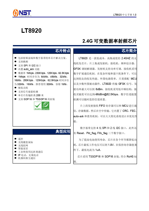
AD892EJP中文资料
- 格式:pdf
- 大小:1.01 MB
- 文档页数:10


Keysight M8920A PXIe Radio Test Set 100 kHz to 3.8/6 GHzField radios are a vital lifeline for warfighters, firefighters andpeacekeepers. That’s why the new Keysight M8920A is designed to deliver the excellence you expect from your radio. All along your lifecycle, we open up capabilities that ranges from deep analysis in design to fast testing in production.Table of ContentsAccelerate MilCom and public safety radio manufacturing (3)Applications (3)Technical Specifications (4)Definitions and conditions (4)RF Analyzer Technical Specifications and Characteristics (5)RF Analyzer Technical Specifications and Characteristics (Continued) (6)RF Generator Technical Specifications and Characteristics (7)RF Generator Technical Specifications and Characteristics (Continued) (8)Audio Module Technical Specifications and Characteristics (8)Audio Module RX Audio Filters (9)Radio Test Application Specifications (9)N9093EM0E basic analog demodulation measurement application key specifications (9)N9093EM1E basic digital demodulation measurement application key specifications (9)Connectivity Test Application Specifications (10)WLAN 802.11ac (10)LTE-FDD/TDD (10)Bluetooth (10)Front Panel M9470A RF Interface Module Connections (10)General Specifications (11)Related Literature (12)Additional Information (12)Accelerate MilCom and public safety radio manufacturingDigital 2-way radios being developed for MilCom and the public safety radio market bring new testing challenges and hurdles to overcome for manufacturers and depot testing. Radio technologies are requiring wider bandwidths, higher frequencies, and multiple radio format capabilities.Product descriptionKeysight’s M8920A PXIe Radio Test Set supports many formats by combining PXI hardware with application-specific software in a single flexible and scalable chassis, providing broad multi-format coverage for next-generation radio testing.With Keysight’s new Radio Test Measurement Application (N9093), you can access and control multiple instruments on one screen while viewing a variety of critical measurements at the same time. Keysight can help deliver the operational excellence you expect from your radio.Applications−Cover all necessary analog AM and FM modulation test requirements.−Test APCO P1/P2, TETRA1, DMR, dPMR, ARIB, and custom modulation formats.−Test commercial connectivity formats including WLAN, LTE, Bluetooth®, etc.−All measurements can be performed with one click of a button.−Test analog Avionics Radios, and your Avionics Databus with optional Databus modulesM8920A PXIe Radio Test SetTechnical SpecificationsDefinitions and conditionsSpecifications describe the warranted performance of calibrated instruments. Data represented in this document are specifications under the following conditions unless otherwise noted.−Specifications are valid from 40° to 65 °C for individual module temperature, as reported by the module, and 20° to 35 °C for environment temperature unless otherwise noted −Calibrated instrument has been stored for a minimum of 2 hours within the allowed operating range−If instrument has previously been stored at a temperature range inside the allowed storage range, but outside the allowed operating range, instrument must have been stored for a minimum of 2hours within the allowed operating range before turn-on−30-minute warm-up time−Calibration cycle maintained−The RF, IF, and Source Alignments have been run within the previous 7 days−An ALL Alignment has been run within the previous 8 hours−If the temperature has changed more than 5 °C from the previous ALL AlignmentTypical describes additional product performance information that is not covered by the product warranty. It is performance beyond specifications that 80% of the units exhibit with a 95% confidence level. This data, shown in italics, does not include measurement uncertainty, and is valid only at room temperature (approximately 25 °C) after alignment within the stated alignment time and temperature limits.Nominal values indicate expected performance or describe product performance that is useful in the application of the product but are not covered by the product warranty.Recommended best practices in use−Use slot blockers and EMC filler panels in empty module slots to ensure proper operating temperatures. Keysight chassis and slot blockers optimize module temperature performance and reliability of test.−Set chassis fan to high at environmental temperatures above 45 °C.RF Analyzer Technical Specifications and Characteristics1.Instantaneous b andwidth (1 d B b andwidth) a vailable a round a c enter frequency o ver w hich t he i nput s ignal c an b e d igitized f or further a nalysis o rprocessing in the time, frequency or modulation domain.2.Calibration a ccuracy d epends o n h ow a ccurately t he f requency s tandard w as a djusted t o 10 M Hz. I f t he a djustment p rocedure i s f ollowed, t he c alibration accuracyis given by the specification. Achievable Initial Calibration Accuracy.3.The 3-dB cutoff frequency can be selected for the User-defined audio filters.RF Analyzer Technical Specifications and Characteristics (Continued)1.T/R port high power attenuation OFF2.Except at 100 MHz, 5 GHz, and 5.5 GHzRF Generator Technical Specifications and Characteristics1.Calibration a ccuracy d epends o n h ow a ccurately t he f requency s tandard w as a djusted t o 10 M Hz. I f t he a djustment p rocedure i s f ollowed, t he c alibrationa ccuracy is given by the specification. Achievable Initial Calibration Accuracy.2. Specifications apply when input port is set to Antenna InRF Generator Technical Specifications and Characteristics (Continued)Audio Module Technical Specifications and CharacteristicsAudio Module RX Audio FiltersRadio Test Application SpecificationsN9093EM0E basic analog demodulation measurement application key specificationsN9093EM1E basic digital demodulation measurement application key specifications1. The 3 dB cutoff frequency can be selected for the User-defined audio filters.Connectivity Test Application SpecificationsWLAN 802.11acLTE-FDD/TDDBluetoothFront Panel M9470A RF Interface Module ConnectionsGeneral SpecificationsFind us at Page 11PPFind us at Page 12Learn more at: For more information on Keysight Technologies’ products, applications or services , please contact your local Keysight office. The complete list is available at: /find/contactusThis information is subject to change without notice. © Keysight Technologies, 2018, Published in USA, Month July 11, 2019, 5992-2802ENRelated LiteratureFor more detailed product and specification information refer to the following literature and web pages: Publication titlePublication number M8920A PXIe Radio Test Set Technical Overview 5992-2821EN M8920A PXIe Radio Test Set Configuration Guide 5992-2800EN M8920A PXIe Radio Test Set Getting Started Guide M8920-90001 M9470A PXIe 50W Interface Module Data Sheet 5992-3140EN M9421A VXT PXIe Vector Transceiver Data Sheet 5992-1646EN M9260A PXIe Audio Analyzer Data Sheet 5992-1918EN PXIe Chassis Spec GuideM9019-90015 PC Tested Configurations with PXIe Chassis Technical Overview 5990-7632EN M9037A PXIe Embedded Controller Spec Guide M9037-90015 Interface Modules and Adapters for PXIe Systems5992-0377EN M924XA InfiniiVision PXIe Modular Oscilloscopes Data Sheet 5992-2003EN 6.5 Digit PXI Digital Multimeter Data Sheet 5992-2757EN PXIe Vector Network Analyzer Configuration Guide 5991-4885EN PXI Avionics Bus Interface Cards Configuration Guide 5992-2448EN 89600 VSA Software Configuration Guide5990-6386ENAdditional InformationProduct webpages:/find/M8920A /find/N9093 /find/PXIX-Series measurement applications: /find/X-Series_AppsSignal Studio Software:/find/signalstudio89600 VSA Software:/find/89600Bluetooth and the Bluetooth logos are trademarks owned byBluetooth SIG, Inc., U.S.A. and licensed to Keysight Technologies, Inc。

Agilent8922MGSM\CDMA手机综合测试仪产品型号: 综合测试仪Agilent8922M产品说明与介绍8922GSM测试装置8922GSM测试装置可以理想地用于R&D、高层维护服务和生产制造方面。
易于使用、丰富而灵活的功能特性使它成为实验台工作选择的仪器。
8922的速度、准确度和重复度使它能够理想地用于来货输入检验和大量生产方面。
8922包括一个GSM基站仿真器及所有信令和测量的能力,能够全面地测试移动台而无需任何附加设备。
GSM无线电测试解决方案8922是一套完整的测试GSM无线台射频部分的测量仪器。
除了频率易变的0.3GMSK 射频发生器外,RF分析仪还有灵活的本地振荡器、相关数据解调节器、脉冲解调器、调频解调器、用于分析相位和频率误差的综合方法分析仪、合成频谱分析仪和脉冲功率计。
8922增加了一个用于完成GSM接收机测量、信道CODEC和呼叫控制协议的误码率测试仪(BERT),以便在进行测量的同时建立电话呼叫并保持链路。
通过用于移动台功能测试的声频CODEC简化了回波模式,并且利用电气人机接口(EMMI)来控制移动台和支持数字音频接口(DAI)。
8922中的快速存储器易于升级。
GSM 数据和HSCSD 测试解决方案8922支持测试GSM单时隙数据和高速电路交换数(HSCSD)移动台的能力。
用在R&D、生产和维修方面,选件K09、K17和K18能够测试单时隙、2x1、2x2、9.6Kb/s和14.4Kb/s 移动数据装置。
完整的成套工具除了完整配套的GSM测量之外,Agilent 8922还包括对于模块测试、排除故障以及调谐作业等有效的通用工具。
这些工具包括一台数字示波器、CW RF合成器、频谱分析仪、CW RF频率计数器、CW和峰值RF功率计、交流电压表、直流电压表、1kHz失真/SINAD(信号对噪声和失真比)测试仪、音频频率计和合成声源。
这些功能的组合使8922对于GSM无线设备的制造和修理都是极为有效的工具。

FLUKE 8922A8920A, 8921A & 8922AAutorangingFluke's autoranging feature allows you to carry out your testing without having to change ranges manually. A range can be placed on HOLD or manually stepped up to a higher range. On HOLD, the meter will remain in a given range regardless of changes in input levels. On STEP UP, the meter will increase ranges step-by-step until the switch is released. Peaking/Dipping MeterIn addition to an accurate digital display, all Fluke Voltmeters in the 8920-Series feature an analog meter for peak and null voltage adjustments. The meter indicates O to 100 percent full scale in each range.Linear Analog OutputModels 8920A and 8922A are equipped with a rear panel output for driving X-Y or st d p chart recorders, delivering voltages proportional to the display count. A 2-volt level equals 2000 counts, a 1-volt level equals 1000 counts, etc. This feature is not available on Model 8921A. AccuracyFluke Digital Voltmeters avoid the possibilities for error so common in analog meters. The digital displays eliminate the likelihood of misreading the meter due to viewing angle problems of parallax common with analog meters. Also, the accuracy of 8920-Series Voltmeters is specified as a percent of reading rather than as percent of full scale.Percent of reading accuracy does not degrade for measurements at the low end of a scale. Front panel switching offers a choice of readings in dB or volts.Technical SpecificationsThe a ccuracy s pecifications b elow apply from 9% to 100% of full scale and from 18°C to 28°C for 90 days. For six-month specifications multiply figures by 1.5.AC Accuracy: ± % of voltage reading or ±dB (8920A/8921 A)Range 2Hz 10 H z 20Hz 50Hz 10 kHz 700V200V1%or 0.5%or 20V 0.15dB 0.1 dB 2V Not200mV Speci-5%orlied 0.5dB 2%or 1%or 20 m V 0.25 d B 0.15dB3%or 2%or 2mV0.35dB 0.25dBAC Accuracy: ± % of voltage reading or ±dB(8922A)Range 2Hz 10 H z 20Hz 50Hz 10 k HzFILTER IN I700V200V 1%or•0.15 d B 1%or 0.5%or20V 0.15 d B 0.1 d B2V 5%or200 mV 3%or• 0.5dB0.35dB2%or•0.25dB 2%or 1%or20 mV 0.25 d B 0.15 d B5%or0.5dB5%or• 5%or 3%or 2%or I2 mv0.5 d B .. 0.5dB 0.35 d B 0.25dB• Valid when AC + DC DAMPING is selected andinput has no de components.••Below 2 mV add number of digits (N) to ±5% voltage readings, where N = 5 + mV input. Or, for dBreadings. add N to ±0.5 dB, where N = 0.5 + (mVinput)2AC+DC Accuracy: Add to AC accuracy specifications (above) ±10 digits or ±0.5 dB above 2mV, or ±100 digits or ±5.0 dB below 2 mV. Forde only, add above digits to 50 Hz to 10 kHzspecificationsFunctions: True RMS measurements only. ACor AC+ DC (8920A and 8921 A); AC or AC+ DCwith damping (8922A)Maximum Input: 700V rms or 1 O OOV peak, not toexceed a volt-hertz product of 1 x 10⁸ on anyrangeMaximum Common Mode Voltage8920A and 8922A: 400 mV rms or 600 mVpeak8921A: 500V rms or 700V peakAC Common Mode Rejection: �60 dB at 50 and60 Hz with 1000 unbalanceDC Common Mode Rejection: �100 dB, 1000unbalanceCrest Factor: 7 at full scale, increasing downscale by 7 times the voltage range divided by thevoltage input. Degrades below 10 Hz, annunciated when capability exceeded (8922A only)Input Impedance: 10 MO shunted by <30 pF200kHz 1 MHz 2MHz 10 M Hz 20MHzNot Specified0.7%or0.15 d B3% o r0.35 d B 5%or0.5dB2%or0.25dB 4%or0.4dB I3%or0.35dB200kHz 1 MHz 2MHz 11 MHzFILTER OUTNot Specified0.7%or0.15 d B3%or0.35 d B2%or 5%or0.25 d B 0.5dB4% o r0.4 d BVoltage R11nges: 2 mV, 20 mV, 200 mV, 2V, 20V,200V, 700VRanging: Autoranging with HOLD to defeat a�to•ranging and STEP UP for manual ranging.Ranges up at 2000 counts and ranges down at180 countsDecibel Ranges: In the autorange mode, theinstrument appears as though it has a singlerange spanning 131 dBdBm Reference: Twelve user-selectable impedances are provided to reference a O dBm, 1mW level (500,750,930, 1100, 1240, 1350,1500, 3000, 6000, 9000, 10000, and 12000)(dBV = 10000)Relative dB Reference: A voltage input presentwhen this button is pushed is held as "O dB"reference point. Subsequent readings indicate±deviations from this pointVoltage Resolution: 0.05% of ranges (3½ digits)Decibel Resolution: O.Q1 dB (4½ digits)Typical-3 dB Points: 40 MHz on 20 mV thru 20Vranges and 4 MHz on 2 mV range (8920A/8921 A); 22 MHz on 2 mV to 20V ranges (8922A)Low Pass Filter: Approximately 200 kHz -3 dBpoint, on 8922A onlyReading Rate: 2.5/s or 1 /s with ac + de withdamping (8922A)Autorange Rate: <950 ms or <3.5s with ac + dewith damping (8922A)Response Time: (To rated accuracy) <1.6s or<7s with ac + de with damping (8922A)Readout: Panel-select able for volts or dB,auto•matic decimal point location: analog peaking/dipping meter. " V .. "V .. "dB,,LED Annunciators: Indicate m , ,"REL REF," and "2 MHz MAX" for 2 mV range(8920A and 8921A) and "UNCAL" when crestfactor limitation exceeded (8922A)Overrange: Flashes maximum reading for thatrangeUnderrange: Flashes decimalLinear Analog Output: (8920A and 8922A only)Linear output of 2000 mV de for a 2000-countreadout; ±1.0% relative to display; essentiallyoo output into a �10 kO load; non-isolated, withoutput common same as input common。


Agilent8920/8921通信测试仪(综测)使用说明一、仪器面板键盘操作及菜单1、面板CRT显示●RX TEST—接收机测试屏幕,可显示RF和AF控制及接收机测试结果。
●TX TEST—发射机测试屏幕,可显示RF和AF控制及发射机测试结果。
●DUPLEX TEST—双工测试屏幕,可同时显示RF和AF控制及收发信机测试结果。
●TESTS—访问来自存储卡、内部ROM/RAM及外接磁盘驱动器装入的程序,可对其编辑与自动运行的屏幕,显示测试结果。
●RF GENERATOR—射频信号源屏幕,用于显示射频与调制信号的控制及测试结果。
●RF ANAL YZER—射频分析仪屏幕,用于显示射频与解调信号的控制及测试结果。
●AF ANAL YZER—音频分析仪屏幕,用于显示音频信号的控制与测试结果。
●OSCILLOSCOPE—示波器屏幕,用于完成对示波器的控制及显示测量结果。
●SPECTRUM ANAL YZER—频谱分析仪屏幕。
●SIGNALING ENCODER—信令编码器屏幕。
●SIGNALING DECODER—信令解码器屏幕。
●RADIO INT—无线电接口与屏幕,显示仪器内置无线电接口卡对外接模块与设备的自动测试结果。
2、面板连接器与控制器●POWER—仪器的电源开关键。
●RF IN/OUT连接器—是一阻抗为50Ω的N型阴性插座,用作射频信号源的输出与调制分析仪的输入接口,允许连续输入60W,或输入100W功率。
●DUPLEX OUT连接器—是一阻抗为50Ω的BNC型阴性插座,用作射频信号源及跟踪信号源的输出端口。
●ANT IN连接器—用作小功率射频信号(≤200Mw)及空中信号的输入端口。
●MIC/ACC接口—是一8针DIN接口,可提供多种用途的连接:MIC IN—当KEY IN接地时去调制射频发生器(先滤波与放大);KEY IN—用于射频信号源的输出开/关状态控制,及在TX TEST与RX TEST屏幕之间的转换控制;KEY OUT1与KEY OUT2用于一部外设的开/关控制。


TA21型牵引变电所安全监控及综合自动化系统说明书WBB-892并补保护测控装置目录1 概述 (59)2 装置功能及特点 (59)3 技术参数 (61)4 结构 (64)5 硬件说明 (64)6 保护原理 (66)7 保护定值及说明 (68)8装置的安装与调试 (70)9 动作信息及说明 (72)10 投运说明及注意事项 (72)11 贮存及保修 (73)12 供货成套性 (73)13 订货须知 (73)14 附图 (73)1 概述WBB-892并补保护测控装置(以下简称装置)是由高性能微处理器实现的并补保护、测量与控制装置。
适用于单相交流电气化铁道牵引供电系统,既可作为常规固定投入并联电容补偿设备的保护、测控装置,也可作为多分支并联电容补偿设备的保护、测控装置。
同时具有负荷录波、故障录波、网络通信等自动化功能。
装置既可单独供货,也可与WKH-892馈线保护测控装置、WBH-892Z主变主保护装置、WBH-892H主变后备保护装置、WBH-892C主变测控装置、WDB-892动力变保护测控装置、WCK-892通用测控装置、WXH-892信号显示装置以及监控系统组成牵引变电所自动化系统。
2装置功能及特点2.1装置功能2.1.1 设计思想在研制过程中,执行相关国际、国家、行业标准,融合多年理论研究成果,吸取既有同类装置成功经验,采纳用户实际需求,融入的设计思想主要有:●装置对调度端、试验仿真工具软件完全透明化设计,便于实现远程诊断;●采用自适应保护原理,克服多支路并补装置投退对保护灵敏度的影响;●采取软件自动调零技术,克服抽取差动电压的电压互感器变比差异对保护动作行为的影响。
2.1.2 保护功能●电流速断保护●过电流保护●谐波过电流保护●差电流保护●差电压保护●过电压保护●低电压保护●谐波阻抗保护●非电量保护2.1.3 测量功能●遥测量—并联电容补偿支路总电流(测量绕组)IM●召测量a)负荷录波☉母线电压☉测量绕组电流b)实时电量☉母线电压☉并联电容补偿支路总电流(保护绕组)☉并联电容补偿支路总电流(测量绕组)☉差电压△U1☉差电压△U2☉差电压△U3☉差电流△I1☉差电流△I2☉差电流△I3c)故障录波☉母线电压☉并联电容补偿支路总电流(保护绕组)d)自检报告☉硬件自检(RAM、A/D、出口驱动等)☉软件自检(整定值校验、程序校验)☉通信自检e)事件报告☉保护由于扰动启动但未出口的信息☉装置“上电”复位信息☉整定值修改f)故障报告2.1.4 控制功能●断路器●隔离开关●装置复归2.1.5遥信功能●“当地”/“遥控”方式开关位置信号●断路器位置信号●断路器手车位置信号●隔离开关位置信号●控制回路断线信号●机构故障信号●装置不良告警●非电量信号(轻瓦斯、电容器过热、动补变过热、动补分闸等)●保护动作信号a)电流速断保护b)过电流保护c)差电流保护d)差电压保护e)过电压保护f)低电压保护g)谐波过电流保护h)谐波阻抗保护i)非电量保护动作信号2.1.6 通信功能●一个可选的光纤Lonworks环网接口,采用插卡方式,可采用单环或冗余双环通信方式,通信速率为1.25Mbps;●一个可选的以太网络接口,采用插卡方式,通信媒介采用光纤,通信速率为10Mbps;●一个标准的RS232串口,用于通过便携机进行日常维护;●一个标准的RS485GPS校时接口。


TDA8920C2× 110 W class-D power amplifierRev. 02 — 11 June 2009Product data sheet1.General descriptionThe TDA8920C is a high-efficiency class-D audio power amplifier. The typical outputpower is 2× 110W with a speaker load impedance of 4Ω.The TDA8920C is available in both HSOP24and DBS23P power packages.The amplifieroperates over a wide supply voltage range from±12.5V to±32.5V and features lowquiescent current consumption.2.FeaturesI Pin compatible with TDA8950/20B for both HSOP24 and DBS23P packagesI Symmetrical operating supply voltage range from±12.5V to±32.5VI Stereo full differential inputs, can be used as stereo Single-Ended (SE) or monoBridge-Tied Load (BTL) amplifierI High output power in typical applications:N SE 2×110W, R L=4Ω (V P =±30V)N SE 2×125W, R L=4Ω (V P =±32V)N SE 2×120W, R L=3Ω (V P =±29V)N BTL 1×220W, R L=8Ω (V P =±30V)I Low noiseI Smooth pop noise-free start-up and switch offI Zero dead time switchingI Fixed frequencyI Internal or external clockI High efficiencyI Low quiescent currentI Advanced protection strategy: voltage protection and output current limitingI Thermal FoldBack (TFB)I Fixed gain of 30dB in SE and 36dB in BTL applicationsI Fully short-circuit proof across loadI BD modulation in BTL configuration3.ApplicationsI DVDI Mini and micro receiverI Home Theater In A Box (HTIAB) systemI High-power speaker system4.Quick reference data[1]V P is the supply voltage on pins VDDP1, VDDP2 and VDDA.[2]The circuit is DC adjusted at V P =±12.5V to ±32.5 V .[3]Output power is measured indirectly; based on R DSon measurement; see Section 13.3.5.Ordering informationTable 1.Quick reference dataSymbol Parameter Conditions Min Typ Max UnitGeneral, V P [1] =±30 V V P supply voltage Operating mode[2]±12.5±30±32.5V V P(ovp)overvoltage protection supply voltage Standby, Mute modes; V DD − V SS65-70V I q(tot)total quiescent currentOperating mode; no load; no filter; no RC-snubber network connected -5075mAStereo single-ended configuration P ooutput powerT j =85°C; L LC =22µH; C LC =680nF (see Figure 10)THD + N =10%; R L =4Ω;V P =±30V[3]-110-W THD + N =10%; R L =4Ω;V P =±27V-90-WMono bridge-tied load configuration P ooutput powerT j =85°C; L LC =22µH; C LC =680nF (see Figure 10); R L =8Ω;THD + N =10%; V P =±30V[3]-220-WTable 2.Ordering informationType numberPackage NameDescriptionVersion TDA8920CJ DBS23P plastic DIL-bent-SIL power package; 23 leads (straight lead length 3.2 mm)SOT411-1TDA8920CTHHSOP24plastic, heatsink small outline package; 24 leads; low stand-off heightSOT566-36.Block diagramPin numbers in brackets refer to type number TDA8920CJ.Fig 1.Block diagram001aai852OUT1V SSP1V DDP2DRIVER HIGH OUT2BOOT2TDA8920CTH (TDA8920CJ)BOOT1DRIVER LOWSWITCH1CONTROL ANDHANDSHAKEPWM MODULATORMANAGEROSCILLATORTEMPERATURE SENSOR CURRENT PROTECTION VOLTAGE PROTECTIONSTABIMODEINPUT STAGE mute9 (3)8 (2)IN1M IN1P22 (15)21 (14)20 (13)17 (11)16 (10)15 (9)VSSP2VSSP1DRIVER HIGH DRIVER LOWSWITCH2CONTROL ANDHANDSHAKEPWM MODULATOR11 (5)n.c.7 (1)OSC 2 (19)SGND6 (23)MODEINPUT STAGEmute5 (22)4 (21)IN2MIN2P 19 (-)24 (17)VSSD n.c.1 (18)VSSA 12 (6)n.c.3 (20)VDDA10 (4)n.c.23 (16)13 (7)18 (12)14 (8)VDDP2PROT STABI VDDP17.Pinning information7.1PinningFig 2.Pin configuration TDA8920CTH Fig 3.Pin configuration TDA8920CJTDA8920CTHVSSD VSSA VDDP2SGND BOOT2VDDA OUT2IN2M VSSP2IN2P n.c.MODE STABI OSC VSSP1IN1P OUT1IN1MBOOT1n.c.VDDP1n.c.PROT n.c.001aai853242322212019181716151413111291078563412TDA8920CJOSC IN1P IN1M n.c.n.c.n.c.PROT VDDP1BOOT1OUT1VSSP1STABI VSSP2OUT2BOOT2VDDP2VSSD VSSA SGND VDDA IN2M IN2P MODE 001aai85412345678910111213141516171819202122237.2Pin descriptionTable 3.Pin descriptionSymbol Pin DescriptionTDA8920CTH TDA8920CJVSSA118negative analog supply voltageSGND219signal groundVDDA320positive analog supply voltageIN2M421channel 2 negative audio inputIN2P522channel 2 positive audio inputMODE623mode selection input: Standby, Mute or OperatingmodeOSC71oscillator frequency adjustment or tracking inputIN1P82channel 1 positive audio inputIN1M93channel 1 negative audio inputn.c.104not connectedn.c.115not connectedn.c.126not connectedPROT137decoupling capacitor for protection (OCP)VDDP1148channel 1 positive power supply voltageBOOT1159channel 1 bootstrap capacitorOUT11610channel 1 PWM outputVSSP11711channel 1 negative power supply voltageST ABI1812decoupling of internal stabilizer for logic supplyn.c.19-not connectedVSSP22013channel 2 negative power supply voltageOUT22114channel 2 PWM outputBOOT22215channel 2 bootstrap capacitorVDDP22316channel 2 positive power supply voltageVSSD2417negative digital supply voltage8.Functional description8.1GeneralThe TDA8920C is a two-channel audio power amplifier that uses class-D technology.For each channel, the audio input signal is converted into a digital PWM signal using ananalog input stage and a PWM modulator; see Figure1. To drive the output powertransistors, the digital PWM signal is fed to a control and handshake block and to high-and low-side driver circuits.This level-shifts the low-power digital PWM signal from a logiclevel to a high-power PWM signal switching between the main supply lines.A2nd-order low-passfilter converts the PWM signal to an analog audio signal that can beused to drive a loudspeaker.The TDA8920C single-chip class-D amplifier contains high-power switches,drivers,timing and handshaking between the power switches, along with some control logic. To ensure maximum system robustness, an advanced protection strategy has been implemented to provide overvoltage, overtemperature and overcurrent protection.Each of the two audio channels contains a PWM modulator,an analog feedback loop and a differential input stage.The TDA8920C also contains circuits common to both channels such as the oscillator, all reference sources, the mode interface and a digital timing manager.The two independent amplifier channels feature high output power, high efficiency, low distortion and low quiescent currents, and can be connected in the followingconfigurations:•Stereo Single-Ended (SE)•Mono Bridge-Tied Load (BTL)The amplifier system can be switched to one of three operating modes using pin MODE:•Standby mode: featuring very low quiescent current•Mute mode: the amplifier is operational but the audio signal at the output is suppressed by disabling the voltage-to-current (VI) converter input stages •Operating mode:the amplifier is fully operational,de-muted and can deliver an output signalA slowly rising voltage should be applied(e.g.via an RC network)to pin MODE to ensure pop noise-free start-up. The bias-current setting of the (VI converter) input stages is related to the voltage on the MODE pin.In Mute mode, the bias-current setting of the VI converters is zero (VI converters are disabled). In Operating mode, the bias current is at a maximum. The time constant required to apply the DC output offset voltage gradually between Mute and Operating mode levels can be generated using an RC network connected to pin MODE.An example of a switching circuit for driving pin MODE is illustrated in Figure4. If the capacitor was omitted, the very short switching time constant could result in audible pop noises being generated at start-up (depending on the DC output offset voltage and loudspeaker used).Fig 4.Example of mode selection circuit010aaa552 SGND mode controlmute/ operating 10 µF5.6 kΩ+5 V470 Ωstandby/ operating S2S1 5.6 kΩTo ensure the coupling capacitors at the inputs (C IN in Figure 10)are fully charged before the outputs start switching,a delay is inserted during the transition from Mute to Operating mode.An overview of the start-up timing is provided in Figure 5.For proper switch-off,the MODE pin should be forced LOW at least 100ms before the supply lines (V DDA and V SSA )drop below 12.5 V .(1)First 1⁄4 pulse down.Upper diagram: When switching from Standby to Mute, there is a delay of approximately 100 ms before the output starts switching.The audio signal will become available once V MODE reaches the Operating mode level (see Table 8),but not earlier than 150ms after switching to Mute.T o start-up pop noise-free, it is recommended that the time constant applied to pin MODE be at least 350 ms for the transition between Mute and Operating modes.Lower diagram: When switching directly from Standby to Operating mode, there is a delay of 100ms before the outputs start switching. The audio signal becomes available after a second delay of 50ms.To start-up pop noise-free,it is recommended that the time-constant applied to pin MODE be at least 500ms for the transition between Standby and Operating modes.Fig 5.Timing on mode selection input pin MODE2.2 V < V MODE < 3 Vaudio outputoperatingstandbymute50 %duty cycle> 4.2 V0 V (SGND)time001aah657V MODE100 ms50 msmodulated PWM> 350 ms2.2 V < V MODE < 3 Vaudio outputoperatingstandbymute50 %duty cycle> 4.2 V0 V (SGND)timeV MODE100 ms50 msmodulated PWM> 350 ms(1)(1)8.2Pulse-width modulation frequencyThe amplifier output signal is a PWM signal with a typical carrier frequency of between250kHz and450kHz.A2nd-order LC demodulationfilter on the output is used to convert the PWM signal into an analog audio signal. The carrier frequency is determined by anexternal resistor, R OSC, connected between pins OSC and VSSA. The optimal carrierfrequency setting is between 250kHz and 450kHz.The carrier frequency is set to345kHz by connecting an external30kΩresistor between pins OSC and VSSA. See Table9 on page14 for more details.If two or more class-D amplifiers are used in the same audio application, it isrecommended that an external clock circuit be used with all devices (see Section13.4).This will ensure that they operate at the same switching frequency, thus avoiding beattones(if the switching frequencies are different,audible interference known as‘beat tones’can be generated)8.3ProtectionThe following protection circuits are incorporated into the TDA8920C:•Thermal protection:–Thermal FoldBack (TFB)–OverT emperature Protection (OTP)•OverCurrent Protection (OCP)•Window Protection (WP)•Supply voltage protection:–UnderVoltage Protection (UVP)–OverVoltage Protection (OVP)–UnBalance Protection (UBP)How the device reacts to a fault conditions depends on which protection circuit has beenactivated.8.3.1Thermal protectionThe TDA8920C employes an advanced thermal protection strategy. A TFB functiongradually reduces the output power within a defined temperature range.If the temperature continues to rise, OTP is activated to shut down the device completely.8.3.1.1Thermal FoldBack (TFB)If the junction temperature(T j)exceeds the thermal foldback activation threshold,the gain is gradually reduced.This reduces the output signal amplitude and the power dissipation, eventually stabilizing the temperature.TFB is specified at the thermal foldback activation temperature T act(th_fold) where theclosed-loop voltage gain is reduced by 6dB. The TFB range is:T act(th_fold)−5°C < T act(th_fold) < T act(th_prot)The value of T act(th_fold) for the TDA8920C is approximately 153°C; see Table8 for moredetails.8.3.1.2OverTemperature Protection (OTP)If TFB fails to stabilize the temperature and the junction temperature continues to rise,the amplifier will shut down as soon as the temperature reaches the thermal protectionactivation threshold,T act(th_prot).The amplifier will resume switching approximately 100ms after the temperature drops below T act(th_prot).The thermal behavior is illustrated in Figure 6.8.3.2OverCurrent Protection (OCP)In order to guarantee the robustness of the TDA8920C, the maximum output current that can be delivered at the output stages is limited. OCP is built in for each output power switch.OCP is activated when the current in one of the power transistors exceeds the OCPthreshold (I ORM = 9.2 A) due, for example, to a short-circuit to a supply line or across the load.The TDA8920C amplifier distinguishes between low-ohmic short-circuit conditions and other overcurrent conditions such as a dynamic impedance drop at the loudspeaker. The impedance threshold (Z th ) depends on the supply voltage.How the amplifier reacts to a short circuit depends on the short-circuit impedance:•Short-circuit impedance >Z th :the amplifier limits the maximum output current to I ORMbut the amplifier does not shut down the PWM outputs. Effectively, this results in a clipped output signal across the load (behavior very similar to voltage clipping).•Short-circuit impedance <Z th :the amplifier limits the maximum output current to I ORMand at the same time discharges the capacitor on pin PROT. When C PROT is fully discharged, the amplifier shuts down completely and an internal timer is started.The value of the protection capacitor (C PROT ) connected to pin PROT can be between 10pF and 220pF (typically 47pF). While OCP is activated, an internal current source is enabled that will discharge C PROT .(1)Duty cycle of PWM output modulated according to the audio input signal.(2)Duty cycle of PWM output reduced due to TFB.(3)Amplifier is switched off due to OTP .Fig 6.Behavior of TFB and OTP001aah656(T act(th_fold) − 5°C)T act(th_fold) T j (°C)T act(th_prot)Gain (dB)30 dB24 dB0 dB123When OCP is activated, the power transistors are turned off. They are turned on again during the next switching cycle.If the output current is still greater than the OCP threshold,they will be immediately switched off again.This switching will continue until C PROT is fully discharged. The amplifier will then be switched off completely and a restart sequence initiated.After a fixed period of 100ms, the amplifier will attempt to switch on again, but will fail if the output current still exceeds the OCP threshold. The amplifier will continue trying to switch on every 100 ms. The average power dissipation will be low in this situation because the duty cycle is low.Switching the amplifier on and off in this way will generate unwanted ‘audio holes’. This can be avoided by increasing the value of C PROT (up to 220 pF) to delay amplifier switch-off. C PROT will also prevent the amplifier switching off due to transient frequency-dependent impedance drops at the speakers.The amplifier will switch on, and remain in Operating mode, once the overcurrent condition has been removed. OCP ensures the TDA8920C amplifier is fully protected against short-circuit conditions while avoiding audio holes.[1]OVP can be triggered by supply pumping; see Section 13.6.8.3.3Window Protection (WP)Window Protection (WP)checks the conditions at the output terminals of the power stage and is activated:•During the start-up sequence, when the TDA8920C is switching from Standby toMute.Start-up will be interrupted If a short-circuit is detected between one of the output terminals and pin VDDP1/VDDP2or VSSP1/VSSP2.The TDA8920C will wait until the short-circuit to the supply lines has been removed before resuming start-up.The short circuit will not generate large currents because the short-circuit check is carried out before the power stages are enabled.•When the amplifier is shut down completely because the OCP circuit has detected ashort circuit to one of the supply lines.WP will be activated when the amplifier attempts to restart after 100 ms (seeSection 8.3.2).The amplifier will not start-up again until the short circuit to the supply lines has been removed.Table 4.Current limiting behavior during low output impedance conditions at different values of C PROTTypeV P (V)V I (mV , p-p) f (Hz)C PROT (pF)PWM output stopsShort (Z th =0Ω)Short(Z th =0.5Ω)Short(Z th =1Ω)TDA8920C 29.55002010yes yes OVP [1]100010yes yes no 2015yes yes OVP [1]100015yes no no 1000220nonono8.3.4Supply voltage protectionIf the supply voltage drops below the minimum supply voltage threshold,V P(uvp),the UVP circuit will be activated and the system will shut down. Once the supply voltage rises above V P(uvp) again, the system will restart after a delay of 100ms.If the supply voltage exceeds the maximum supply voltage threshold, V P(ovp), the OVP circuit will be activated and the power stages will be shut down. When the supply voltage drops below V P(ovp) again, the system will restart after a delay of 100ms.An additional UnBalance Protection (UBP) circuit compares the positive analog supply voltage (on pin VDDA) with the negative analog supply voltage (on pin VSSA) and is triggered if the voltage difference exceeds a factor of two (V DDA > 2×|V SSA | OR |V SSA |>2× V DDA ). When the supply voltage difference drops below the unbalance threshold,V P(ubp), the system restarts after 100ms.An overview of all protection circuits and their respective effects on the output signal is provided in T able 5.[1]Amplifier gain depends on the junction temperature and heatsink size.[2]The amplifier shuts down completely only if the short-circuit impedance is below the impedance threshold (Z th ; see Section 8.3.2). In all other cases, current limiting results in a clipped output signal.[3]Fault condition detected during any Standby-to-Mute transition or during a restart after OCP has been activated (short-circuit to one of the supply lines).8.4Differential audio inputsThe audio inputs are fully differential ensuring a high common mode rejection ratio and maximum flexibility in the application.•Stereo operation: to avoid acoustical phase differences, the inputs should be inantiphase and the speakers should be connected in antiphase. This configuration:–minimizes power supply peak current–minimizes supply pumping effects, especially at low audio frequencies•Mono BTL operation:the inputs must be connected in anti-parallel.The output of onechannel is inverted and the speaker load is connected between the two outputs of the TDA8920C. In practice (because of the OCP threshold) the output power can be boosted to twice the output power that can be achieved with the single-ended configuration.The input configuration for a mono BTL application is illustrated in Figure 7.Table 5.Overview of TDA8920C protection circuitsProtection name Completeshutdown Restart directly Restart after 100ms Pin PROT detection TFB [1]N N N N OTP Y N Y N OCP Y [2]N [2]Y [2]Y WP N [3]Y N N UVP Y N Y N OVP Y N Y N UBPYNYN9.Limiting values[1]V P is the supply voltage on pins VDDP1, VDDP2 and VDDA.10.Thermal characteristicsFig 7. Input configuration for mono BTL applicationV inIN1P OUT1power stagembl466OUT2SGNDIN1MIN2P IN2MTable 6.Limiting valuesIn accordance with the Absolute Maximum Rating System (IEC 60134).Symbol Parameter ConditionsMin Max Unit V P [1]supply voltageStandby, Mute modes; V DD − V SS -65V I ORM repetitive peak output current maximum output current limiting9.2-A T stg storage temperature −55+150°C T amb ambient temperature −40+85°C T j junction temperature -150°C V MODE voltage on pin MODE referenced to SGND06V V OSC voltage on pin OSC 0SGND + 6V V I input voltage referenced to SGND; pin IN1P; IN1M;IN2P and IN2M−5+5V V PROT voltage on pin PROTreferenced to voltage on pin VSSD 012V V ESD electrostatic discharge voltage Human Body Model (HBM)−2000+2000V Charged Device Model (CDM)−500+500V I q(tot)total quiescent current Operating mode; no load; no filter; no RC-snubber network connected -75mA V PWM(p-p)peak-to-peak PWM voltageon pins OUT1 and OUT2-120VTable 7.Thermal characteristics Symbol ParameterConditions Typ Unit R th(j-a)thermal resistance from junction to ambient in free air40K/W R th(j-c)thermal resistance from junction to case1.1K/W11.Static characteristics[1]V P is the supply voltage on pins VDDP1, VDDP2 and VDDA.[2]The circuit is DC adjusted at V P =±12.5V to ±32.5 V .[3]Unbalance protection activated when V DDA > 2×|V SSA | OR |V SSA |> 2× V DDA .[4]With respect to SGND (0V).[5]The transition between Standby and Mute modes has hysteresis,while the slope of the transition between Mute and Operating modes is determined by the time-constant of the RC network on pin MODE; see Figure 8.[6]DC output offset voltage is gradually applied to the output during the transition between Mute and Operating modes. The slope caused by any DC output offset is determined by the time-constant of the RC network on pin MODE.[7]At a junction temperature of approximately T act(th_fold)−5°C,gain reduction commences and at a junction temperature of approximately T act(th_prot),the amplifier switches off.Table 8.Static characteristics V P [1] =±30 V; f osc = 345 kHz; T amb = 25°C; unless otherwise specified.Symbol Parameter Conditions Min Typ Max Unit Supply V P supply voltageOperating mode [2]±12.5±30±32.5V V P(ovp)overvoltage protection supply voltageStandby, Mute modes;V DD −V SS65-70V V P(uvp)undervoltage protection supply voltage V DD −V SS 20-25V V P(ubp)unbalance protection supply voltage [3]-33-%I q(tot)total quiescent currentOperating mode; no load; no filter;no RC-snubber network connected -5075mAI stb standby current measured at 30 V -480650µA Mode select input; pin MODEV MODEvoltage on pin MODEreferenced to SGND [4]0-6V Standby mode [4][5]0-0.8V Mute mode [4][5] 2.2- 3.0V Operating mode[4][5]4.2-6V I I input current V I =5.5 V -110150µA Audio inputs; pins IN1M, IN1P , IN2P and IN2MV I input voltage DC input [4]-0-V Amplifier outputs; pins OUT1 and OUT2V O(offset)output offset voltageSE; Mute mode --±25mV SE; Operating mode [6]--±150mV BTL; Mute mode --±30mV BTL; Operating mode[6]--±210mV Stabilizer output; pin STABI V O(STABI)output voltage on pin ST ABIMute and Operating modes;with respect to VSSD9.39.810.3VTemperature protection T act(th_prot)thermal protection activation temperature-154-°C T act(th_fold)thermal foldback activation temperatureclosed loop SE voltage gain reduced with 6dB[7]-153-°C12.Dynamic characteristics12.1Switching characteristics[1]V P is the supply voltage on pins VDDP1, VDDP2 and VDDA.[2]When using an external oscillator, the frequency f track (500 kHz minimum, 900 kHz maximum) will result in a PWM frequency f osc (250kHz minimum, 450 kHz maximum) due to the internal clock divider; see Section 8.2.[3]When t r(i) > 100 ns, the output noise floor will increase.Fig 8. Behavior of mode selection pin MODEStandbyMuteOn5.5coa021V MODE (V)4.23.02.20.80V O (V)V O(offset)(mute)V O(offset)(on)slope is directly related to the time-constantof the RC network on the MODE pinTable 9.Dynamic characteristics V P [1] =±30 V; T amb = 25°C; unless otherwise specified.Symbol Parameter Conditions Min Typ Max Unit Internal oscillatorf osc(typ)typical oscillator frequency R OSC =30.0k Ω290345365kHz f osc oscillator frequency 250-450kHz External oscillator input or frequency tracking; pin OSCV OSC voltage on pin OSC HIGH-levelSGND +4.5SGND +5SGND +6V V trip trip voltage -SGND + 2.5-V f track tracking frequency [2]500-900kHz Z i input impedance 1--M ΩC i input capacitance --15pF t r(i)input rise timefrom SGND +0V toSGND + 5 V[3]--100ns12.2Stereo SE configuration characteristics[1]R sL is the series resistance of the low-pass LC filter inductor used in the application.[2]Output power is measured indirectly; based on R DSon measurement; see Section 13.3.[3]THD measured between 22Hz and 20kHz,using AES1720kHz brick wall filter;max.limit is guaranteed but may not be 100%tested.[4]V ripple = V ripple(max) = 2 V (p-p); measured independently between VDDPn and SGND and between VSSPn and SGND.[5]22 Hz to 20 kHz, using AES17 20 kHz brick wall filter.[6]22 Hz to 20 kHz, using AES17 20 kHz brick wall filter.[7]P o = 1 W; f i = 1kHz.[8]V i = V i(max) = 1 V (RMS); f i = 1 kHz.[9]Leads and bond wires included.Table 10.Dynamic characteristicsV P =±30 V; R L = 4Ω; f i = 1 kHz; f osc = 345 kHz; R sL [1] < 0.1Ω; T amb = 25°C; unless otherwise specified.Symbol Parameter ConditionsMin Typ Max Unit P ooutput powerL =22µH; C LC =680nF; T j =85°C [2]THD =0.5%; R L = 4Ω-90-W THD =10%; R L = 4Ω-110-W THD =10%; V P =±27 V-90-W THD total harmonic distortion P o =1W; f i =1kHz [3]-0.05-%P o =1W; f i =6kHz[3]-0.05-%G v(cl)closed-loop voltage gain 293031dB SVRRsupply voltage ripple rejectionbetween pins VDDPn and SGND Operating mode; f i =100Hz [4]-90-dB Operating mode; f i =1kHz [4]-70-dB Mute mode; f i =100Hz [4]-75-dB Standby mode; f i =100Hz [4]-120-dB between pins VSSPn and SGND Operating mode; f i =100Hz [4]-80-dB Operating mode; f i =1kHz [4]-60-dB Mute mode; f i =100Hz [4]-80-dB Standby mode; f i =100Hz[4]-115-dB Z i input impedance between one of the input pins and SGND4563-k ΩV n(o)output noise voltage Operating mode; R s =0Ω[5]-160-µV Mute mode[6]-85-µV αcs channel separation [7]-70-dB |∆G v |voltage gain difference --1dB αmute mute attenuationf i =1kHz; V i =2V (RMS)[8]-75-dB CMRR common mode rejection ratio V i(CM)=1V (RMS)-75-dB ηpooutput power efficiencySE, R L = 4Ω-88-%SE, R L = 6Ω-90-%BTL, R L = 8Ω-88-%R DSon(hs)high-side drain-source on-state resistance [9]-200-m ΩR DSon(ls)low-side drain-source on-state resistance[9]-190-m Ω12.3Mono BTL application characteristics[1]R sL is the series resistance of the low-pass LC filter inductor used in the application.[2]Output power is measured indirectly; based on R DSon measurement; see Section 13.3.[3]THD measured between 22Hz and 20kHz,using AES1720kHz brick wall filter;max.limit is guaranteed but may not be 100%tested.[4]V ripple = V ripple(max) = 2 V (p-p).[5]22 Hz to 20 kHz, using an AES17 20 kHz brick wall filter; low noise due to BD modulation.[6]22 Hz to 20 kHz, using an AES17 20 kHz brick wall filter.[7]V i = V i(max) = 1 V (RMS); f i = 1 kHz.Table 11.Dynamic characteristicsV P =±30 V; R L = 8Ω; f i = 1 kHz; f osc = 345 kHz; R sL [1] < 0.1Ω ; T amb = 25°C; unless otherwise specified.Symbol Parameter ConditionsMin Typ Max UnitP ooutput powerT j =85°C;L LC =22µH;C LC =680nF (see Figure 10)[2]THD =0.5%; R L = 8Ω-170-W THD =10%; R L = 8Ω-220-W THD total harmonic distortion P o =1W; f i =1kHz [3]-0.05-%P o =1W; f i =6kHz[3]-0.05-%G v(cl)closed-loop voltage gain -36-dB SVRRsupply voltage ripple rejectionbetween pin VDDPn and SGND Operating mode; f i =100Hz [4]-80-dB Operating mode; f i =1kHz [4]-80-dB Mute mode; f i =100Hz [4]-95-dB Standby mode; f i =100Hz [4]-120-dB between pin VSSPn and SGND Operating mode; f i =100Hz [4]-75-dB Operating mode; f i =1kHz [4]-75-dB Mute mode; f i =100Hz [4]-90-dB Standby mode; f i =100Hz[4]-130-dB Z i input impedance measured between one of the input pins and SGND4563-k ΩV n(o)output noise voltage Operating mode; R s =0Ω[5]-190-µV Mute mode[6]-45-µV αmute mute attenuationf i =1kHz; V i =2V (RMS)[7]-75-dB CMRRcommon mode rejection ratioV i(CM)=1V (RMS)-75-dB。

产品特点:●标准的CMOS工艺●嵌入512K/256位EPROM●21/10秒语音长度其标准是在6KHz采样率和4位ADPCM压缩下。
●最大12段语音●组合声音块来扩展语音持续时间●有960个入口表供语音块组合●语音数据存储8位PCM或4位ADPCM压缩可供用户选择●两种触发模式的使用(EPROM设计选择)—(Key Trigger Mode)按键触发模式:S1-S4组合触发12组语音,也可以通过SBT键顺序触发语音组—(CPU Parallel Trigger)CPU并口触发模式:S1-S4组合选择12组语音地址通过STB触发对应地址语音组●语音组触发选择:(Edge / Level)上升沿触发/高电平触发;(Hold / Un-hold)保持/不保持;(Retrigger / Non-retrigger)覆盖/不覆盖●芯片全局选择:(Ramp / No-ramp)斜坡/无斜坡;(Output Options)输出选择;( Key / CPU)按键/CPU触发模式●16ms(基于8KHz采样率)延时在按键触发模式时●65us(基于8KHz采样率)延时在CPU并口模式时●RST脚置高语音立即停止播放●两个用户可设计输出,其中选择有:停止时输出脉冲,忙信号,LED 闪烁●内置振荡器通过外接电阻来控制采样率● 2.6-5.0V范围内单电源供电和<5uA低耗静态。
●PWM输出,VOUT1脚和VOUT2脚直接驱动喇叭●D/A输出,COUT脚通过晶体管驱动喇叭●开发系统支持语音的编辑和选择产品说明:aP8921A/10A系列是高性能的嵌入512K/256位EPROM的标准CMOS工艺的OTP语音芯片。
基于6Khz的采样率和4位ADPCM压缩它能存储21/10秒长度的语音信息。
同时8位的PCM数据存储供用户选择。
简单按键触发和CPU并口触发两种模式便于不同需求的用户选择。
外接电阻控制振荡频率,8位D/A电流输出和PWM直推输出最小化外接元件。