Power Semiconductor Devices and Smart Power ICs
- 格式:doc
- 大小:2.18 MB
- 文档页数:10
The semiconductor industry, often referred to as the backbone of modern technology, has seen exponential growth over the past few decades. It is a crucial component in various electronic devices, including smartphones, computers, medical equipment, and automotive systems. This summary aims to provide an overview of the key aspects of the semiconductor industry, its evolution, current state, and future prospects.Evolution of the Semiconductor IndustryThe history of the semiconductor industry dates back to the late 1940s when the first semiconductor device, the Point Contact Transistor, was invented. However, it was the invention of the Junction Transistor by William Shockley in 1947 that marked the beginning of the modern semiconductor era. Over the years, advancements in semiconductor technology have led to the miniaturization of devices, improved performance, and reduced costs.The development of integrated circuits (ICs) in the late 1950s and early 1960s revolutionized the industry. These circuits, which integrated thousands of transistors onto a single chip, paved the way for thedigital revolution. The advancements continued with the transition from small-scale integration (SSI) to medium-scale integration (MSI), large-scale integration (LSI), and eventually to very large-scale integration (VLSI) and ultra-large-scale integration (ULSI).Current State of the Semiconductor IndustryToday, the semiconductor industry is a multi-billion-dollar global market. It is characterized by fierce competition, rapid technological innovation, and high capital investment. The industry is segmented into various categories, including microprocessors, memory devices, analog devices, and discrete semiconductors.1. Microprocessors: These are the central processing units (CPUs) that power computers and other electronic devices. Companies like Intel, AMD, and ARM dominate this segment.2. Memory Devices: This category includes Dynamic Random-Access Memory (DRAM) and Static Random-Access Memory (SRAM), which are essential forstoring data. Samsung, SK Hynix, and Micron are key players in this segment.3. Analog Devices: These devices handle analog signals and are used in various applications, such as power management, signal conditioning, and audio processing. Texas Instruments, Analog Devices, and ON Semiconductor are leading companies in this area.4. Discrete Semiconductors: These are individual semiconductor devices, such as diodes, transistors, and thyristors, which are used in a wide range of applications. Infineon, ON Semiconductor, and NXP Semiconductors are prominent in this segment.Challenges and OpportunitiesThe semiconductor industry faces several challenges, including supply chain disruptions, geopolitical tensions, and increasing demand for advanced technologies. However, these challenges also present opportunities for innovation and growth.1. Supply Chain Disruptions: The COVID-19 pandemic highlighted the vulnerabilities of global supply chains. To mitigate this risk, companies are looking to diversify their supply chains and invest in local production facilities.2. Geopolitical Tensions: Trade wars and geopolitical tensions have created uncertainties in the semiconductor industry. Companies are navigating these challenges by establishing strategic partnerships and diversifying their operations.3. Advanced Technologies: The industry is increasingly focusing on advanced technologies such as 5G, artificial intelligence (AI), and the Internet of Things (IoT). These technologies are expected to drive demand for semiconductors and create new markets.Future ProspectsThe future of the semiconductor industry looks promising, with continuous advancements in technology and increasing demand for electronic devices. Key trends include:1. 5G Technology: The rollout of 5G networks will require more advanced and efficient semiconductors to support the high data throughput and low latency requirements.2. AI and IoT: The integration of AI and IoT into various devices will drive the need for more powerful and energy-efficient semiconductors.3. Green Technology: As the world moves towards sustainability, the semiconductor industry is focusing on developing energy-efficient devices and recycling processes.In conclusion, the semiconductor industry has come a long way since its inception and continues to evolve at a rapid pace. With ongoing technological advancements and increasing demand, the industry is poised for continued growth and innovation in the coming years.。
肖特基势垒光电二极管原理及应用------------------------------------------------------------------------------------------------肖特基势垒光电二极管原理及应用姜凤贤1 王燕涛1 马军辉2(1.燕山大学里仁学院实验中心河北秦皇岛 066004;2.国家广电总局 2022台新疆喀什 844000)摘要: 详细介绍肖特基势垒二极管的工作原理、特性及应用,简单介绍肖特基势垒光电二极管的工作原理及应用展望。
关键词: 肖特基势垒二极管;肖特基势垒光电二极管;原理应用中图分类号:TN311.7 文献标识码:A 文章编号:1671,7597(2011)0820122,020 引言肖特基势垒光电二极管又称金属-半导体光电二极管,其势垒不再是p-n结,而是金属和半导体接触形成的阻挡层,即肖特基势垒。
1 肖特基势垒二极管结构原理及特性1.1 简述图1 肖特基势垒二极管肖特基二极管(如图1)是以其发明人肖特基博士(Schottky)命名的,SBD是肖特基势垒二极管(Schottky Barrier Diode,缩写成SBD)的简称。
SBD不是利用p 型半导体与n型半导体接触形成p-n结原理制作的,而是利用金属与半导体接触形成的金属,半导体结原理制作的。
因此,SBD也称为金属-半导体(接触)二极管或表面势垒二极管,它是一种热载流子二极管。
是近年来问世的低功耗、大电流、超高速半导体器件。
其反向恢复时间极短(可以小到几纳秒),——————————————————————————————————————------------------------------------------------------------------------------------------------正向导通压降仅0.4V左右,而整流电流却可达到几千安培。
FlashPro4 Device ProgrammerQuickstart CardKit ContentsQuantity Description1FlashPro4 programmer standalone unit1USB A to mini-B USB cable1FlashPro4 10-pin ribbon cable1Quickstart cardHardware InstallationAfter installing the software successfully, connect one end of the USB cable to the FlashPro4 device programmer and the other end to your PC’s USB port. The Found Hardware Wizard will open twice. Use the wizard to install the driver automatically (recommended). If the Found Hardware Wizard cannot find the drivers automatically, then ensure you have properly installed the FlashPro software prior to installing the hardware. If the drivers still cannot be installed automatically, then install them from a list or specific location (advanced).If FlashPro was installed as part of the Libero IDE default installation, the drivers are located atC:/Libero/Designer/Drivers/Manual. For a standalone FlashPro default installation, the drivers are located at C:/Microsemi/FlashPro/Drivers/Manual. Microsemi recommends the automatic driver installation. Note: FlashPro4 uses pin 4 of the JTAG connector, whereas FlashPro3 had no connection to this pin. FlashPro4 pin 4 of the JTAG header is a PROG_MODE output drive signal. PROG_MODE toggles between programming and normal operation. The PROG_MODE signal is intended to drive an N or P Channel MOSFET to control the output of a voltage regulator between the programming voltage of 1.5 V and normal operation voltage of 1.2 V. This is required for ProASIC®3L, IGLOO® V2, and IGLOO PLUS V2 devices because, although they can operate at 1.2 V, they must be programmed with a VCC core voltage of 1.5 V. For all other devices, leave this pin (PIN4 - PROG_MODE) unconnected (NC). For more information, see FlashPro4 Backward Compatibility with FlashPro3.Pin 4 on FlashPro4 programmers must not be connected or used for other than their intended purpose.1Microsemi, a wholly owned subsidiary of Microchip Technology Inc. (Nasdaq: MCHP), offers a comprehensive portfolio of semiconductor and system solutions for aerospace & defense, communications, data center and industrial markets. Products include high-performance and radiation-hardened analog mixed-sig nal integ rated circuits, FPGAs, SoCs and ASICs; power manag ement products; timing and synchronization devices and precise time solutions, setting the world's standard for time; voice processing devices; RF solutions; discrete components; enterprise storage and communication solutions, security technologies and scalable anti-tamper products; Ethernet solutions; Power-over-Ethernet ICs and midspans; as well as custom design capabilities and services. Learn more at .Microsemi HeadquartersOne Enterprise, Aliso Viejo, CA 92656 USAWithin the USA: +1 (800) 713-4113Outside the USA: +1 (949) 380-6100Sales: +1 (949) 380-6136Fax: +1 (949) 215-4996email:*************************** Microsemi makes no warranty, representation, or guarantee regarding the information contained herein or the suitability of its products and services for any particular purpose, nor does Microsemi assume any liability whatsoever arising out of the application or use of any product or circuit. The products sold hereunder and any other products sold by Microsemi have been subject to limited testing and should not be used in conjunction with mission-critical equipment or applications. Any performance specifications are believed to be reliable but are not verified, and Buyer must conduct and complete all performance and other testing of the products, alone and together with, or installed in, any end-products. Buyer shall not rely on any data and performance specifications or parameters provided by Microsemi. It is the Buyer’s responsibility to independently determine suitability of any products and to test and verify the same. The information provided by Microsemi hereunder is provided “as is, where is” and with all faults, and the entire risk associated with such information is entirely with the Buyer. Microsemi does not grant, explicitly or implicitly, to any party any patent rights, licenses, or any other IP rights, whether with regard to such information itself or anything described by such information. Information provided in this document is proprietary to Microsemi, and Microsemi reserves the right to make any changes to the information in this document or to any products and services at any time without notice.©2016–2018 Microsemi, a wholly owned subsidiary of Microchip Technology Inc. All rights reserved. Microsemi and the Microsemi logo are registered trademarks ofMicrosemi Corporation. All other trademarks and service marks are the property of their respective owners.50200198. 3.00. 08/18note.Software and LicensingLibero ® SoC Design Suite offers high productivity with its comprehensive, easy-to-learn, easy-to-adopt development tools for designing with Microsemi’s low power Flash FPGAs and SoC. The suite integrates industry standard Synopsys Synplify Pro ® synthesis and Mentor Graphics ModelSim ® simulation with best-in-class constraints management and debug capabilities.Download the latest Libero SoC release/products/fpga-soc/design-resources/design-software/libero-soc#downloads Generate a Libero Silver license for your kit/products/fpga-soc/design-resources/licensingDocumentation ResourcesFor more information about the FlashPro4 Device Programmer, see the documentation at/product-directory/programming/4977-flashpro#documentsSupportTechnical support is available online at /soc/support and by email at**********************Microsemi sales offices, including representatives and distributors, are located worldwide.To find your local representative, go to /salescontacts。
行业分类代码集成电路设计英文版Industry Classification Code: Integrated Circuit DesignIntegrated circuit design is a crucial segment within the electronics industry, playing a pivotal role in the development of modern technology. This article aims to explore the industry classification code for integrated circuit design, highlighting its significance, applications, and future prospects.Industry ClassificationIntegrated circuit design falls under the broader umbrella of the electronics industry, specifically within the semiconductor and electronics component manufacturing sector. The industry classification code for integrated circuit design typically varies depending on the international or regional standards used for classification. For instance, in the United States, the Standard Industrial Classification (SIC) code for this sector would be 3674- Semiconductor and Other Electronic Component Manufacturing.Significance of Integrated Circuit DesignIntegrated circuits (ICs) are the backbone of modern electronics, serving as the foundation for a wide range of devices and systems. IC design involves creating the layout and specifications for these circuits, ensuring their functionality, reliability, and performance. The importance of IC design lies in its ability to influence the efficiency, cost, and scalability of electronic products across multiple industries, including but not limited to consumer electronics, telecommunications, medical devices, automotive, and aerospace.Applications of Integrated Circuit DesignThe applications of integrated circuit design are vast and diverse. ICs are found in smartphones, computers, and other consumer electronics, enabling their advanced features and functionality. In the telecommunications industry, ICs power base stations, routers, and other equipment that facilitate globalconnectivity. In the medical field, ICs are used in diagnostic equipment, implantable devices, and remote monitoring systems, improving patient care and outcomes. Additionally, ICs play a crucial role in the automotive industry, enabling features like fuel efficiency, safety systems, and infotainment.Future ProspectsThe future of integrated circuit design looks bright, with continued advancements in technology driving new opportunities and challenges. The increasing demand for smaller, faster, and more energy-efficient ICs is driving innovation in materials, design techniques, and manufacturing processes. The emergence of new technologies like 5G, artificial intelligence, and the Internet of Things is expected to further expand the market for IC design, opening up new areas of application and growth.In conclusion, the industry classification code for integrated circuit design represents a crucial segment within the electronics industry. The significance of IC design lies in itsability to shape the future of technology across multiple industries, driving innovation and progress. With the continuous evolution of technology, the future prospects for integrated circuit design are exciting and full of potential.中文版行业分类代码:集成电路设计集成电路设计是电子工业中的关键领域,在现代技术的发展中扮演着重要的角色。
CMOS工艺简要概述(英文版)CMOS technology, short for Complementary Metal-Oxide-Semiconductor technology, is a popular integrated circuit manufacturing process used in the production of digital logic ICs, microprocessors, and many other electronic devices.The CMOS technology relies on the use of both n-type and p-type metal-oxide-semiconductor field-effect transistors (MOSFETs) to create a complementary circuitry design. This means that both types of transistors operate together to achieve lower power consumption, higher speed, and enhanced noise immunity.The fabrication process of CMOS technology begins with the preparation of a silicon substrate, which is then oxidized to create a thin layer of silicon dioxide (SiO2). This oxide layer acts as an insulating material and helps to isolate the transistors from the substrate. Next, a layer of polysilicon is deposited on the oxide layer, which will eventually serve as the gate electrode of the MOSFETs.Afterwards, a process called photolithography is used to define the transistor regions on the substrate. A layer of photoresist is applied to the substrate and exposed to ultraviolet light through a photomask, which contains the desired circuit pattern. The exposed photoresist is then developed, leaving behind a patterned layer that protects certain areas of the substrate.Using the patterned photoresist layer as a mask, various etching techniques are employed to remove unwanted materials from the substrate. This step helps to form the source and drain regions ofthe MOSFETs, as well as other interconnects and contacts required for circuit connectivity.Once the transistor regions are defined, dopants are introduced into the substrate through ion implantation or diffusion processes. These dopants alter the electrical properties of the substrate, creating n-type and p-type regions that form the active regions of the transistors.Following the doping step, a thin layer of insulating material called the inter-metal dielectric (IMD) is deposited on the substrate, and contact vias are created to connect the transistors with the metal interconnect layers. Metal interconnect layers, typically made of aluminum or copper, are then deposited and patterned to form the desired circuit connections.Finally, a passivation layer is applied to protect the integrated circuit from environmental factors and ensure its reliability.In summary, CMOS technology is a versatile and widely used fabrication process for the production of integrated circuits. Through a combination of precise material deposition, patterning, doping, and interconnect formation steps, CMOS technology enables the creation of complex and high-performance digital electronic devices.CMOS技术在集成电路制造中的广泛应用源于其独特的特性和优势。
图标/网站名称网址简单介绍21IC中国电子网电子工程师的网站 (嵌入式系统,单片机,DSP,EDA,测试测量,元器件,通信,电源,微电子,半导体)。
430开发网 430开发网。
51单片机世界 51单片机世界。
单片机世界单片机世界欢迎你!学单片机这里是入口。
世纪开发网世纪开发网。
单片机爱好者单片机爱好者。
超前科技超前科技CQKJ单片机仿真器产品专栏 C51仿真器,keil C51仿真机。
平凡单片机工作室单片机教学与学习网站。
单片机工作室单片机工作室。
51开发网 51开发网。
51新手交易网 51新手交易网。
孙冠单片机孙冠单片机。
嵌入开发网嵌入开发网。
老古开发网单片机与嵌入式系统专业网站。
晓奇工作室老古开发网。
单片机学习网晓奇工作室。
利舒技术实验室利舒技术实验室。
Xmcu 单片机工作室单片机网单片机知识、实验板、编程仿真工。
PIC学习网单片机,编程器,仿真器,单片机学习,PIC单片机原理,PIC单片机简介,PIC单片机字习,PIC单片机资料。
小龙微控小龙微控--个人网站。
51测试网 51测试网。
致祥电子致祥电子。
电子制作实验室电子制作实验室。
亦峰电子亦峰电子。
DevARM 开发网 DevARM 开发网。
超业电子超业电子。
龙人电子龙人电子。
中国电子技术信息网单片机,嵌入式系统,IC,EDA,元器件,电路,电源,通信,测量,编程,仿真,SMS,GPRS,ISP,电子论坛,软件下载,信息发布。
电子工程师网站单片机,FPGA,嵌入式系统,电路板设计。
单片机C语言C51BBS论坛单片机C语言C51BBS论坛。
中国IC网 IC信息发布比高科技比高科技。
北京仪器商城生产销售仪器,仪器仪表,国内大型仪器企业,仪器仪表商城 www_17web_com亿涛电子设计工作室亿涛电子设计工作室。
单片机坐标单片机 C51 单片机C语言 C语言原代码单片机毕业论文单片机毕业设计源代码芯片驱动程序基本电路设计 AVR单片机单片机人才推荐哈工大实验编程工具下载实用工具。
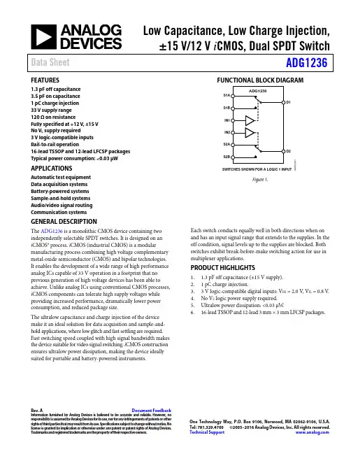
Low Capacitance, Low Charge Injection,±15 V/12 V i CMOS, Dual SPDT Switch Data Sheet ADG1236Rev. A Document FeedbackInformation furnished by Analog Devices is believed to be accurate and reliable. However, noresponsibility is assumed by Analog Devices for its use, nor for any infringements of patents or other rights of third parties that may result from its use. Specifications subject to change without notice. No license is granted by implication or otherwise under any patent or patent rights of Analog Devices. T rademarks and registered trademarks are the property of their respective owners. One Technology Way, P.O. Box 9106, Norwood, M A 02062-9106, U.S.A. Tel: 781.329.4700 ©2005–2016 Analog Devices, Inc. All rights reserved. Technical Support FEATURES1.3 pF off capacitance3.5 pF on capacitance1 pC charge injection33 V supply range120 Ω on resistanceFully specified at +12 V, ±15 VNo V L supply required3 V logic-compatible inputsRail-to-rail operation16-lead TSSOP and 12-lead LFCSP packages Typical power consumption: <0.03 µW APPLICATIONSAutomatic test equipmentData acquisition systemsBattery-powered systemsSample-and-hold systemsAudio/video signal routing Communication systemsFUNCTIONAL BLOCK DIAGRAM SWITCHES SHOWN FOR A LOGIC 1 INPUT04776-1Figure 1.GENERAL DESCRIPTIONThe ADG1236 is a monolithic CMOS device containing two independently selectable SPDT switches. It is designed on ani CMOS® process. i CMOS (industrial CMOS) is a modular manufacturing process combining high voltage complementary metal-oxide semiconductor (CMOS) and bipolar technologies. It enables the development of a wide range of high performance analog ICs capable of 33 V operation in a footprint that no previous generation of high voltage devices has been able to achieve. Unlike analog ICs using conventional CMOS processes, i CMOS components can tolerate high supply voltages while providing increased performance, dramatically lower power consumption, and reduced package size.The ultralow capacitance and charge injection of the device make it an ideal solution for data acquisition and sample-and-hold applications, where low glitch and fast settling are required. Fast switching speed coupled with high signal bandwidth makes the device suitable for video signal switching. i CMOS construction ensures ultralow power dissipation, making the device ideally suited for portable and battery-powered instruments. Each switch conducts equally well in both directions when on and has an input signal range that extends to the supplies. In the off condition, signal levels up to the supplies are blocked. Both switches exhibit break-before-make switching action for use in multiplexer applications.PRODUCT HIGHLIGHTS1. 1.3 pF off capacitance (±15 V supply).2. 1 pC charge injection.3. 3 V logic-compatible digital inputs: V IH = 2.0 V, V IL = 0.8 V.4.No V L logic power supply required.5.Ultralow power dissipation: <0.03 µW.6.16-lead TSSOP and 12-lead 3 mm × 3 mm LFCSP packages.ADG1236Data SheetRev. A | Page 2 of 16TABLE OF CONTENTSFeatures .............................................................................................. 1 Applications ....................................................................................... 1 Functional Block Diagram .............................................................. 1 General Description ......................................................................... 1 Product Highlights ........................................................................... 1 Revision History ............................................................................... 2 Specifications ..................................................................................... 3 Dual Supply ................................................................................... 3 Single Supply ................................................................................. 5 Absolute Maximum Ratings ............................................................6 ESD Caution...................................................................................6 Truth Table for Switches ...............................................................6 Pin Configurations and Function Descriptions ............................7 Terminology .......................................................................................8 Typical Performance Characteristics ..............................................9 Test Circuits ..................................................................................... 12 Outline Dimensions ....................................................................... 14 Ordering Guide .. (14)REVISION HISTORY3/16—Rev. 0 to Rev. AChanges to Figure 2 and Figure 3 ................................................... 7 Updated Outline Dimensions ....................................................... 14 Changes to Ordering Guide . (14)9/05—Revision 0: Initial VersionData SheetADG1236Rev. A | Page 3 of 16SPECIFICATIONSDUAL SUPPLYV DD = 15 V ± 10%, V SS = −15 V ± 10%, GND = 0 V , unless otherwise noted. Table 1.Y V e rsion 1 Parameters 25°C −40°C to +85°C −40°C to +125°C Unit Test Conditions/Comments 1 ANALOG SWITCH Analog Signal Range V DD to V SS V On Resistance (R ON ) 120 Ω typ V S = ±10 V, I S = −1 mA; Figure 20 190 230 260 Ω max V DD = +13.5 V, V SS = −13.5 VOn Resistance Match BetweenChannels (∆R ON )3.5 Ω typ V S = ±10 V, I S = −1 mA 6 10 12 Ω max On Resistance Flatness (R FLAT(ON)) 20 Ω typ V S = −5 V, 0 V, +5 V; I S = −1 mA 57 72 79 Ω max LEAKAGE CURRENTS V DD = +16.5 V, V SS = −16.5 V Source Off Leakage, I S (Off) ±0.02 nA typ V S = ±10 V, V S = ∓10 V; Figure 21 ±0.1 ±0.6 ±1 nA max Drain Off Leakage, I D (Off) ±0.02 nA typ V S = ±10 V, V S = ∓10 V; Figure 21 ±0.1 ±0.6 ±1 nA max Channel On Leakage, I D , I S (On) ±0.02 nA typ V S = V D = ±10 V; Figure 22 ±0.2 ±0.6 ±1 nA max DIGITAL INPUTS Input High Voltage, V INH 2.0 V min Input Low Voltage, V INL 0.8 V max Input Current, I INL or I INH 0.005 μA typ V IN = V INL or V INH ±0.1 μA max Digital Input Capacitance, C IN 2 pF typ DYNAMIC CHARACTERISTICS 2 Transition Time, t TRANS A OFF B ON 125 ns typ R L = 300 Ω, C L = 35 pF 150 200 ns max V S = 10 V; Figure 23 Transition Time, t TRANS B OFF A ON 70 ns typ R L = 300 Ω, C L = 35 pF 90 115 ns max V S = 10 V; Figure 23 Break-Before-Make Time Delay, t D 25 ns typ R L = 300 Ω, C L = 35 pF 10 ns min V S1 = V S2 = 10 V; Figure 24 Charge Injection −1 pC typ V S = 0 V, R S = 0 Ω, C L = 1 nF; Figure 25 Off Isolation 80 dB typ R L = 50 Ω, C L = 5 pF, f = 1 MHz;Figure 26Channel-to-Channel Crosstalk 85 dB typ R L = 50 Ω, C L = 5 pF, f = 1 MHz;Figure 27Total Harmonic Distortion + Noise 0.15 % typ R L = 10 kΩ, 5 V rms, f = 20 Hz to20 kHz−3 dB Bandwidth 1000 MHz typ R L = 50 Ω, C L = 5 pF; Figure 28 C S (Off) 1.3 pF typ f = 1 MHz; V S = 0 V 1.6 pF max f = 1 MHz; V S = 0 V C D , C S (On) 3.5 pF typ f = 1 MHz; V S = 0 V 4.3 pF max f = 1 MHz; V S = 0 VADG1236Data SheetRev. A | Page 4 of 16Y Version 1Parameters25°C −40°C to +85°C −40°C to +125°C Unit Test Conditions/Comments 1 POWER REQUIREMENTSV DD = +16.5 V, V SS = −16.5 V I DD 0.001 µA typ Digital inputs = 0 V or V DD 1.0 µA maxI DD 170 µA typ Digital inputs = 5 V230 µA maxI SS 0.001 µA typ Digital inputs = 0 V or V DD1.0 µA maxI SS 0.001 µA typ Digital inputs = 5 V1.0µA max1 Temperature range for Y version is −40°C to +125°C. 2Guaranteed by design; not subject to production test.Data SheetADG1236Rev. A | Page 5 of 16SINGLE SUPPLYV DD = 12 V ± 10%, V SS = 0 V , GND = 0 V , unless otherwise noted. Table 2.Y Version 1Parameters25°C −40°C to +85°C −40°C to +125°C Unit Test Conditions/Comments ANALOG SWITCHAnalog Signal Range 0 V to V DD VOn Resistance (R ON ) 300 Ω typ V S = 0 V to 10 V, I S = −1 mA; Figure 20475 567 625 Ω max V DD = 10.8 V, V SS = 0 VOn Resistance Match Between Channels (∆R ON ) 4.5 Ω typ V S = 0 V to 10 V, I S = −1 mA16 26 27 Ω maxOn Resistance Flatness (R FLAT(ON)) 60 Ω typ V S = 3 V, 6 V, 9 V, I S = −1 mA LEAKAGE CURRENTSV DD = 13.2 VSource Off Leakage, I S (Off) ±0.02 nA typ V S = 1 V/10 V, V D = 10 V/1 V; Figure 21±0.1 ±0.6 ±1 nA maxDrain Off Leakage, I D (Off) ±0.02 nA typ V S = 1 V/10 V, V D = 10 V/1 V; Figure 21±0.1 ±0.6 ±1 nA maxChannel On Leakage, I D , I S (On) ±0.02 nA typ V S = V D = 1 V or 10 V, Figure 22±0.2 ±0.6 ±1 nA max DIGITAL INPUTSInput High Voltage, V INH 2.0 V min Input Low Voltage, V INL0.8 V maxInput Current, I INL or I INH 0.001µA typ V IN = V INL or V INH±0.1 µA max Digital Input Capacitance, C IN 3 pF typ DYNAMIC CHARACTERISTICS 2Transition Time, t TRANS B OFF A ON 105 ns typ R L = 300 Ω, C L = 35 pF140 175 ns max V S = 8 V; Figure 23 Transition Time, t TRANS A OFF B ON 155 ns typ R L = 300 Ω, C L = 35 pF190 255 ns max V S = 8 V; Figure 23 Break-Before-Make Time Delay, t D 50 ns typ R L = 300 Ω, C L = 35 pF10 ns min V S1 = V S2 = 8 V; Figure 24Charge Injection −0.8 pC typ V S = 6 V, R S = 0 Ω, C L = 1 nF; Figure 25 Off Isolation75 dB typ R L = 50 Ω, C L = 5 pF, f = 1 MHz; Figure 26; Channel-to-Channel Crosstalk 85 dB typ R L = 50 Ω, C L = 5 pF, f = 1 MHz; Figure 27 −3 dB Bandwidth 800 MHz typ R L = 50 Ω, C L = 5 pF; Figure 28 C S (Off) 1.6 pF typ f = 1 MHz; V S = 6 V1.9 pF max f = 1 MHz; V S = 6 V C D , C S (On) 4 pF typ f = 1 MHz; V S = 6 V4.9 pF max f = 1 MHz; V S = 6 V POWER REQUIREMENTSV DD = 13.2 VI DD 0.001 µA typ Digital inputs = 0 V or V DD 1.0 µA maxI DD 170 µA typ Digital inputs = 5 V230µA max1 Temperature range for Y version is −40°C to +125°C. 2Guaranteed by design; not subject to production test.ADG1236Data SheetRev. A | Page 6 of 16ABSOLUTE MAXIMUM RATINGST A = 25°C, unless otherwise noted. Table 3.Parameter Rating V DD to V SS 35 VV DD to GND −0.3 V to +25 V V SS to GND +0.3 V to −25 VAnalog Inputs 1 V SS − 0.3 V to V DD + 0.3 V or 30 mA, whichever occurs first Digital Inputs 1 GND − 0.3 V to V DD + 0.3 V or 30 mA, whichever occurs first Peak Current, S or D100 mA (pulsed at 1 ms, 10% duty cycle max) Continuous Current per Channel, S or D25 mAOperating Temperature RangeAutomotive (Y Version) −40°C to +125°C Storage Temperature Range −65°C to +150°C Junction Temperature150°C 16-Lead TSSOP , θJA Thermal Impedance112°C/W 12-Lead LFCSP , θJA Thermal Impedance80°C/W Reflow Soldering Peak Temperature, Pb Free260°C1Over voltages at IN, S, or D are clamped by internal diodes. Current must be limited to the maximum ratings given.Stresses at or above those listed under Absolute Maximum Ratings may cause permanent damage to the product. This is a stress rating only; functional operation of the product at these or any other conditions above those indicated in the operational section of this specification is not implied. Operation beyond the maximum operating conditions for extended periods may affect product reliability.ESD CAUTIONTRUTH TABLE FOR SWITCHESTable 4.IN Switch A Switch B 0 Off On 1OnOffData SheetADG1236Rev. A | Page 7 of 16PIN CONFIGURATIONS AND FUNCTION DESCRIPTIONSIN1S1A D1S1B V SS GND NC NCNC NC NC V DD S2BD2S2A IN204776-002NC = NO CONNECT. DO NOT CONNECT TO THIS PIN.Figure 2. TSSOP Pin ConfigurationNOTES1.NC = NO CONNECT. DO NOT CONNECT TO THIS PIN.2. THE EXPOSED PAD MUST BE TIED TO SUBSTRATE, V SS .04776-003987123V DD S2B D2D1S1B V SS 4G N D 5I N 26S 2A2S 1A1I N 10N CFigure 3. LFCSP Pin ConfigurationTable 5. Pin Function DescriptionsPin No.TSSOP LFCSP Mn e monic D e scription 1 11 IN1 Logic Control Input. 2 12 S1A Source Terminal. Can be an input or output. 3 1 D1 Drain Terminal. Can be an input or output. 4 2 S1B Source Terminal. Can be an input or output. 5 3 V SS Most Negative Power Supply Potential. 6 4 GND Ground (0 V) Reference. 7, 8, 14 to 16 10 NC No Connect. 9 5 IN2 Logic Control Input. 10 6 S2A Source Terminal. Can be an input or output. 11 7 D2 Drain Terminal. Can be an input or output. 12 8 S2B Source Terminal. Can be an input or output. 13 9 V DD Most Positive Power Supply Potential.ADG1236Data SheetRev. A | Page 8 of 16TERMINOLOGYI DDThe positive supply current. I SSThe negative supply current.V D (V S )The analog voltage on Terminals D and S. R ONThe ohmic resistance between D and S.R FLAT(ON)Flatness is defined as the difference between the maximum and minimum value of on resistance as measured over the specified analog signal range.I S (Off)The source leakage current with the switch off. I D (Off)The drain leakage current with the switch off. I D , I S (On)The channel leakage current with the switch on. V INLThe maximum input voltage for Logic 0. V INHThe minimum input voltage for Logic 1. I INL (I INH )The input current of the digital input.C S (Off)The off switch source capacitance, measured with reference to ground. C D (Off)The off switch drain capacitance, measured with reference to ground. C D , C S (On)The on switch capacitance, measured with reference to ground. C INThe digital input capacitance.t TRANSThe delay time between the 50% and 90% points of the digital input and switch on condition when switching from one address state to another.Charge InjectionA measure of the glitch impulse transferred from the digital input to the analog output during switching.Off IsolationA measure of unwanted signal coupling through an off switch. CrosstalkA measure of unwanted signal that is coupled through from one channel to another as a result of parasitic capacitance. BandwidthThe frequency at which the output is attenuated by 3 dB. On ResponseThe frequency response of the on switch. Insertion LossThe loss due to the on resistance of the switch.THD + NThe ratio of the harmonic amplitude plus noise of the signal to the fundamental.Data SheetADG1236Rev. A | Page 9 of 16TYPICAL PERFORMANCE CHARACTERISTICSSOURCE OR DRAIN VOLTAGE (V)O N R E S I S T A N C E (Ω)200100018016014012080604020Figure 4. On Resistance as a Function of V D (V S) for Dual SupplySOURCE OR DRAIN VOLTAGE (V)O N R E S I S T A N C E (Ω)6003000500400200100Figure 5. On Resistance as a Function of V D (V S ) for Dual SupplySOURCE OR DRAIN VOLTAGE (V)O N R E S I S T A N C E (Ω)4502503000Figure 6. On Resistance as a Function of V D (V S ) for Single SupplyTEMPERATURE (°C)O N R E S I S T A N C E (Ω)250004776-01415020010050Figure 7. On Resistance as a Function of V D (V S ) for Different Temperatures,Dual SupplyTEMPERATURE (°C)O N R E S I S T A N C E (Ω)60004776-015300400200500100Figure 8. On Resistance as a Function of V D (V S ) for Different Temperatures,Single SupplyTEMPERATURE (°C)L E A K A G E (n A )0.20–0.2004776-01600.050.100.15–0.05–0.15–0.10Figure 9. Leakage Currents as a Function of Temperature, Dual SupplyADG1236Data SheetRev. A | Page 10 of 16TEMPERATURE (°C)L E A K A G E (n A )0.35–0.10Figure 10. Leakage Currents as a Function of Temperature, Single SupplyLOGIC, IN X (V)I D D (µA )605040301020Figure 11. I DD vs. Logic LevelV BIAS (V)C H A R G E I N J E C T I O I N (p C )642–2–4–6 Figure 12. Charge Injection vs. Source VoltageTEMPERATURE (°C)T I M E (n s )22020018016014012010080604020004776-004Figure 13. t TRANSITION Times vs. TemperatureFREQUENCY (Hz)O F F I S O L A T I O N (d B )0–100–90–80–70–60–50–40–30–20–10Figure 14. Off Isolation vs. FrequencyFREQUENCY (Hz)C R O S S T A L K (d B )0–100–90–80–70–60–50–40–30–20–10Figure 15. Crosstalk vs. FrequencyFREQUENCY (Hz)O N R E S P O N S E (d B )–30–10–5–15–20–25Figure 16. On Response vs. FrequencyFREQUENCY (Hz)T H D + N (%)10.001.000.100.01Figure 17. THD + N vs. FrequencyV BIAS (V)C A P A C I T A N C E (p F )54321004776-007Figure 18. Capacitance vs. Source Voltage for Dual SupplyV BIAS (V)C A P A C I T A N C E (p F )5431204776-006Figure 19. Capacitance vs. Source Voltage for Single SupplyTEST CIRCUITSV S04776-020Figure 20. Test Circuit 1—On ResistanceV S04776-021Figure 21. Test Circuit 2—Off Resistance04776-022Figure 22. Test Circuit 3—On Leakage04776-023OUTV V V VFigure 23. Test Circuit 4—Switching Times04776-024OUTV VV VBBM BBMV OUTV INFigure 24. Test Circuit 5—Break-Before-Make Time DelayV IN (NORMALLY CLOSED SWITCH)V OUTV IN OFFON 04776-025OUTV V VFigure 25. Test Circuit 6—Charge Injection04776-026OFF ISOLATION = 20 logV SFigure 26. Test Circuit 7—Off IsolationV V 04776-INSERTION LOSS = 20 logOUT V OUT WITHOUT SWITCHFigure 27. Test Circuit 8—Channel-to-Channel CrosstalkCHANNEL-TO-CHANNEL CROSSTALK = 20 logV OUT ΩV SV 04776-028Figure 28. Test Circuit 9—BandwidthV 04776-029OUTLINE DIMENSIONSCOPLANARITY0.10COMPLIANT TO JEDEC STANDARDS MO-153ABFigure 30. 16-Lead Thin Shrink Small Outline Package [TSSOP](RU-16)Dimensions shown in millimeters1.451.30 SQ 1.15111808-A0.08COMPLIANT TO JEDEC STANDARDS MO-220-WEED.FOR PROPER CONNECTION OF THE EXPOSED PAD, REFER TO THE PIN CONFIGURATION AND FUNCTION DESCRIPTIONSSECTION OF THIS DATA SHEET.0.800.75Figure 31. 12-Lead Lead Frame Chip Scale Package [LFCSP]3 mm × 3 mm Body and 0.75 mm Package Height(CP-12-4)Dimensions shown in millimetersORDERING GUIDEModel 1Temperature Range Package DescriptionPackage Option ADG1236YRUZ−40°C to +125°C 16-Lead Thin Shrink Small Outline Package [TSSOP] RU-16 ADG1236YRUZ-REEL −40°C to +125°C 16-Lead Thin Shrink Small Outline Package [TSSOP] RU-16 ADG1236YRUZ-REEL7 −40°C to +125°C 16-Lead Thin Shrink Small Outline Package [TSSOP] RU-16 ADG1236YCPZ-500RL7 −40°C to +125°C 12-Lead Lead Frame Chip Scale Package [LFCSP] CP-12-4 ADG1236YCPZ-REEL7−40°C to +125°C 12-Lead Lead Frame Chip Scale Package [LFCSP] CP-12-41Z = RoHS Compliant Part.NOTESNOTES©2005–2016 Analog Devices, Inc. All rights reserved. Trademarks and registered trademarks are the property of their respective owners.D04776-0-3/16(A)。
半导体英文词汇SemiconductorA semiconductor is a material that has electrical conductivity between that of a conductor and that of an insulator. This means that it can conduct some electricity under certain conditions, but not as much as a conductor. Semiconductors are essential components of electronic devices, such as diodes, transistors, and integrated circuits.半导体半导体是一种在导体和绝缘体之间具有电导性的材料。
这意味着在某些条件下它可以导电,但不像导体那样能够导电。
半导体是电子器件的基本组成部分,如二极管、晶体管和集成电路。
DiodeA diode is a semiconductor device that allows current to flow in only one direction. It has two terminals, an anode and a cathode. When a positive voltage is applied to the anode and a negative voltage to the cathode, the diode conducts electricity. However, if the polarity of theapplied voltage is reversed, the diode blocks the flow of current.二极管二极管是一种只允许电流在一个方向中流动的半导体器件。

1.5KE160CA-E3/54 1.5KE47CA-E3/541.5KE6.8A thru 1.5KE540A, 1N6267A thru 1N6303AVishay General SemiconductorT RANS Z ORB ® Transient Voltage SuppressorsDEVICES FOR BI-DIRECTION APPLICATIONSFor bi-directional types, use CA suffix (e.g. 1.5KE220CA) Electrical characteristics apply in both directions.FEATURES•Glass passivated chip junction•Available in uni-directional and bi-directional •1500 W peak pulse power capability with a 10/1000 μs waveform, repetitive rate (duty cycle): 0.01 %•Excellent clamping capability •Very fast response time•Low incremental surge resistance•AEC-Q101 qualified•Solder dip 275 °C max. 10 s, per JESD 22-B106•Material categorization: for definitions of compliance please see /doc?99912TYPICAL APPLICATIONSUse in sensitive electronics protection against voltage transients induced by inductive load switching and lighting on ICs, MOSFET, signal lines of sensor units for consumer, computer, industrial, automotive, and telecommunication.MECHANICAL DATACase: molded epoxy body over passivated junction Molding compound meets UL 94 V-0 flammability rating Base P/N-E3 - RoHS compliant, commercial gradeBase P/NHE3_X - RoHS compliant, and AEC-Q101 qualified (“X” denotes revision code e.g. A, B, ...)Terminals: matte tin plated leads, solderable per J-STD-002 and JESD 22-B102E3 suffix meets JESD 201 class 1A whisker test, HE3 suffix meets JESD 201 class 2 whisker testNote• 1.5KE250A to 1.5KE540A are commercial grade only•Bi-directional is available from 1.5KE6.8CA to 1.5KE220CA onlyPolarity: For uni-directional types the color band denotes cathode end, no marking on bi-directional typesNotes(1)Non-repetitive current pulse, per fig. 3 and derated above T A= 25 °C per fig. 2(2)Measured on 8.3 ms single half sine-wave or equivalent square wave, duty cycle = 4 pulses per minute maximum (3)V F = 3.5 V for 1.5KE220A and below; V F= 5.0 V for 1.5KE250A and above PRIMARY CHARACTERISTICSV BR uni-directional 6.8 V to 540 V V BR bi-directional 6.8 V to 220 V V WM uni-directional 5.8 V to 459 V V WM bi-directional5.8 V to 185 V P PPM 1500 W P D6.5 W I FSM (uni-directional only)200 A T J max.175 °CPolarity Uni-directional, bi-directionalPackage1.5KEMAXIMUM RATINGS (T A = 25 °C unless otherwise noted)PARAMETERSYMBOL VALUE UNIT Peak pulse power dissipation with a 10/1000 μs waveform (1) (fig. 1)P PPM 1500W Peak pulse current with a 10/1000 μs waveform (1) I PPM See next tableA Power dissipation on infinite heatsink at T L = 75 °C (fig. 5)P D 6.5W Peak forward surge current 8.3 ms single half sine-wave uni-directional only (2)I FSM 200A Maximum instantaneous forward voltage at 100 A for uni-directional only (3) V F 3.5/5.0V Operating junction and storage temperature rangeT J , T STG-55 to +175°C1.5KE6.8A thru 1.5KE540A, 1N6267A thru 1N6303AVishay General SemiconductorNotes(1) Pulse test: t p≤ 50 ms (2) S urge current waveform per fig. 3 and derate per fig. 2(3) All terms and symbols are consistent with ANSI/IEEE CA62.35(4) For bi-directional types with V R 10 V and less the I Dlimit is doubled (+) Underwriters laboratory recognition for the classification of protectors (QVGQ2) under the UL standard for safety 497B and file number E136766 for both uni-directional and bi-directional devicesELECTRICAL CHARACTERISTICS (T A = 25 °C unless otherwise noted)JEDEC ® TYPE NUMBER GENERAL SEMICONDUCTOR PART NUMBER BREAKDOWN VOLTAGE V BR AT I T (1)(V) TEST CURRENT I T (mA)STAND-OFF VOLTAGE V WM (V)MAXIMUM REVERSE LEAKAGE AT V WM I D (4) (μA) MAXIMUM PEAKPULSECURRENT I PPM (2)(A)MAXIMUM CLAMPING VOLTAGE AT I PPM V C (V) MAXIMUM TEMPERATURE COEFFICIENTOF V BR (%/°C)MIN.MAX.1N6267A (+)1.5KE6.8A 6.457.1410 5.80100014310.50.0571N6268A (+)1.5KE7.5A 7.137.8810 6.4050013311.30.0611N6269A (+)1.5KE8.2A 7.798.61107.022*******.10.0651N6270A (+)1.5KE9.1A 8.659.55 1.07.785011213.40.0681N6271A (+)1.5KE10A 9.5010.5 1.08.551010314.50.0731N6272A (+)1.5KE11A 10.511.6 1.09.40 5.096.215.60.0751N6273A (+)1.5KE12A 11.412.6 1.010.2 5.089.816.70.0781N6274A (+)1.5KE13A 12.413.7 1.011.1 5.082.418.20.0811N6275A (+)1.5KE15A 14.315.8 1.012.8 1.070.821.20.0841N6276A (+)1.5KE16A 15.216.8 1.013.6 1.066.722.50.0861N6277A (+)1.5KE18A 17.118.9 1.015.3 1.059.525.20.0891N6278A (+)1.5KE20A 19.021.0 1.017.1 1.054.227.70.0901N6279A (+)1.5KE22A 20.923.1 1.018.8 1.049.030.60.0921N6280A (+)1.5KE24A 22.825.2 1.020.5 1.045.233.20.0941N6281A (+)1.5KE27A 25.728.4 1.023.1 1.040.037.50.0961N6282A (+)1.5KE30A 28.531.5 1.025.6 1.036.241.40.0971N6283A (+)1.5KE33A 31.434.7 1.028.2 1.032.845.70.0981N6284A (+)1.5KE36A 34.237.8 1.030.8 1.030.149.90.0991N6285A (+)1.5KE39A 37.141.0 1.033.3 1.027.853.90.1001N6286A (+)1.5KE43A 40.945.2 1.036.8 1.025.359.30.1011N6287A (+)1.5KE47A 44.749.4 1.040.2 1.023.164.80.1011N6288A (+)1.5KE51A 48.553.6 1.043.6 1.021.470.10.1021N6289A (+)1.5KE56A 53.258.8 1.047.8 1.019.577.00.1031N6290A (+)1.5KE62A 58.965.1 1.053.0 1.017.685.00.1041N6291A (+)1.5KE68A 64.671.4 1.058.1 1.016.392.00.1041N6292A (+)1.5KE75A 71.378.8 1.064.1 1.014.61040.1051N6293A (+)1.5KE82A 77.986.1 1.070.1 1.013.31130.1051N6294A (+)1.5KE91A 86.595.5 1.077.8 1.012.01250.1061N6295A (+)1.5KE100A 95.0105 1.085.5 1.010.91370.1061N6296A (+)1.5KE110A 105116 1.094.0 1.09.91520.1071N6297A (+)1.5KE120A 114126 1.0102 1.09.11650.1071N6298A (+)1.5KE130A 124137 1.0111 1.08.41790.1071N6299A (+)1.5KE150A 143158 1.0128 1.07.22070.1061N6300A (+)1.5KE160A 152168 1.0136 1.0 6.82190.1081N6301A (+)1.5KE170A 162179 1.0145 1.0 6.42340.1081N6302A (+)1.5KE180A 171189 1.0154 1.0 6.12460.1081N6303A (+)1.5KE200A 190210 1.0171 1.0 5.52740.108-(+)1.5KE220A 209231 1.0185 1.0 4.63280.108- 1.5KE250A 237263 1.0214 1.0 4.43440.110- 1.5KE300A 285315 1.0256 1.0 3.64140.110- 1.5KE350A 333368 1.0300 1.0 3.14820.110- 1.5KE400A 380420 1.0342 1.0 2.75480.110- 1.5KE440A 418462 1.0376 1.0 2.56020.110- 1.5KE480A 456504 1.0408 1.0 2.286580.110- 1.5KE510A 485535 1.0434 1.0 2.156980.110- 1.5KE540A 513567 1.0459 1.0 2.037400.1101.5KE6.8A thru 1.5KE540A, 1N6267A thru 1N6303A Vishay General Semiconductor Notes(1)AEC-Q101 qualified(2)Applied for 1.5KE6.8AHE3_A to 1.5KE220AHE3_A, and 1.5KE6.8CAHE3_A to 1.5KE220CAHE3_ARATINGS AND CHARACTERISTICS CURVES (T A = 25 °C unless otherwise noted)Fig. 1 - Peak Pulse Power Rating CurveFig. 2 - Pulse Power or Current vs. Initial Junction TemperatureFig. 3 - Pulse WaveformFig. 4 - Typical Junction CapacitanceTHERMAL CHARACTERISTICS (T A = 25 °C unless otherwise noted)PARAMETER SYMBOL VALUE UNIT Typical thermal resistance, junction to ambient RθJA75°C/ W Typical thermal resistance, junction to lead RθJL15.4ORDERING INFORMATION (Example)PREFERRED PIN UNIT WEIGHT (g)PREFERRED PACKAGE CODE BASE QUANTITY DELIVERY MODE1.5KE6.8A-E3/540.96854140013" diameter paper tape and reel 1.5KE6.8AHE3_A/C (1)(2)0.968C140013" diameter paper tape and reel1.5KE6.8A thru 1.5KE540A, 1N6267A thru 1N6303A Vishay General SemiconductorFig. 5 - Power Derating CurveFig. 6 - Maximum Non-Repetitive Forward Surge CurrentUni-Directional onlyFig. 7 - Incremental Clamping Voltage Curve (Uni-Directional)Fig. 8 - Incremental Clamping Voltage Curve (Uni-directional) Fig. 9 - Incremental Clamping Voltage Curve (Bi-directional) Fig. 10 - Incremental Clamping Voltage Curve (Bi-Directional)1.5KE6.8A thru 1.5KE540A, 1N6267A thru 1N6303A Vishay General SemiconductorFig. 11 - Instantaneous Forward Voltage Characteristics Curve Fig. 12 - Typical Transient Thermal Impedance PACKAGE OUTLINE DIMENSIONS in inches (millimeters)APPLICATION NOTES•This series of Silicon Transient Suppressors is used in applications where large voltage transients can permanently damage voltage-sensitive components.•The TVS diode can be used in applications where induced lightning on rural or remote transmission lines presents a hazard to electronic circuitry (ref: R.E.A. specification P.E. 60). •This Transient Voltage Suppressor diode has a pulse power rating of 1500 W for 1 ms. The response time of TVS diode clamping action is effectively instantaneous (1 x 10⁻⁹ s bi-directional); therefore, they can protect integrated circuits, MOS devices, hybrids, and other voltage sensitive semiconductors and components. TVS diodes can also be used in series or parallel to increase the peak power ratings.Legal Disclaimer Notice VishayDisclaimerALL PRODUCT, PRODUCT SPECIFICAT IONS AND DAT A ARE SUBJECT T O CHANGE WIT HOUT NOT ICE T O IMPROVE RELIABILITY, FUNCTION OR DESIGN OR OTHERWISE.Vishay Intertechnology, Inc., its affiliates, agents, and employees, and all persons acting on its or their behalf (collectively, “Vishay”), disclaim any and all liability for any errors, inaccuracies or incompleteness contained in any datasheet or in any other disclosure relating to any product.Vishay makes no warranty, representation or guarantee regarding the suitability of the products for any particular purpose or the continuing production of any product. To the maximum extent permitted by applicable law, Vishay disclaims (i) any and all liability arising out of the application or use of any product, (ii) any and all liability, including without limitation special, consequential or incidental damages, and (iii) any and all implied warranties, including warranties of fitness for particular purpose, non-infringement and merchantability.Statements regarding the suitability of products for certain types of applications are based on Vishay’s knowledge of typical requirements that are often placed on Vishay products in generic applications. Such statements are not binding statements about the suitability of products for a particular application. It is the customer’s responsibility to validate that a particular product with the properties described in the product specification is suitable for use in a particular application. Parameters provided in datasheets and / or specifications may vary in different applications and performance may vary over time. All operating parameters, including typical parameters, must be validated for each customer application by the customer’s technical experts. Product specifications do not expand or otherwise modify Vishay’s terms and conditions of purchase, including but not limited to the warranty expressed therein.Except as expressly indicated in writing, Vishay products are not designed for use in medical, life-saving, or life-sustaining applications or for any other application in which the failure of the Vishay product could result in personal injury or death. Customers using or selling Vishay products not expressly indicated for use in such applications do so at their own risk. Please contact authorized Vishay personnel to obtain written terms and conditions regarding products designed for such applications.No license, express or implied, by estoppel or otherwise, to any intellectual property rights is granted by this document or by any conduct of Vishay. Product names and markings noted herein may be trademarks of their respective owners.© 2017 VISHAY INTERTECHNOLOGY, INC. ALL RIGHTS RESERVED1.5KE160CA-E3/54 1.5KE47CA-E3/54。
高速集电极沟槽绝缘栅双极晶体管蒋梦轩;帅智康;沈征;王俊;刘道广【摘要】在前期高速绝缘栅双极晶体管(IGBT)的基础上提出一种高速集电极沟槽绝缘栅双极晶体管(CT-IGBT).该器件沟槽集电极与漂移区的内建电势差感应形成电子沟道而加快关断速度,且集电极沟槽具有不同于传统电场截止层(FS)的电场截止机制,并引入低浓度N型层以降低集电极沟槽对空穴注入的抑制作用.硅基材料有限元仿真结果表明,新结构CT-IGBT的关断下降时间比传统沟槽FS-IGBT少49%,且前者耐受的雪崩能量比后者高32%.因此,新结构CT-IGBT具有比FS-IGBT更优越的关断速度和强度,可应用于大功率高速电力电子系统.%This paper proposes a novel collector trench insulated gate bipolar transistor (CT-IGBT) with an electron extraction channel formed on the collector side to enhance the electron extraction effect, in which a low doped n-type layer is introduced to increase hole injection efficiency at the collector side. TCAD simulation indicates that the proposed IGBT structure offers a turn-off fall time 49% lower and avalanche energy 32% higher than a conventional field-stop IGBT (FS-IGBT). Therefore, the proposed IGBT is attractive for high-speed and large-power electronic converters.【期刊名称】《电工技术学报》【年(卷),期】2017(032)024【总页数】6页(P53-58)【关键词】绝缘栅双极晶体管;电场截止;关断下降时间;雪崩能量;强度【作者】蒋梦轩;帅智康;沈征;王俊;刘道广【作者单位】输配电装备及系统安全与新技术国家重点实验室(重庆大学) 重庆400044;湖南大学电气与信息工程学院长沙 410082;湖南大学电气与信息工程学院长沙 410082;湖南大学电气与信息工程学院长沙 410082;清华大学核能与新能源研究院北京 100084【正文语种】中文【中图分类】TM46目前,产业化的高电压大功率绝缘栅双极晶体管(Insulated Gate Bipolar Transistor, IGBT)普遍采用新结构设计制造技术,以ABB、三菱、东芝和日立等为代表的国际领先研发制造公司均采用了新结构设计制造技术,如软穿通技术、注入增强门极晶体管(Injection Enhanced Gate Transistor, IEGT)技术、载流子存储增强技术和平面注入增强技术等[1-4]。
700V nLDMOS击穿电压参数设计文燕;张枫;李天贺;李娜【摘要】为了不增加器件成本,方便和低压器件集成到一起时实现自主隔离,因而迫切需要解决既能兼容普通半导体材料工艺又能达到相应技术性能要求的器件设计.为此设计了一种采用NWELL而非N-外延层作为nLDMOS的漂移区,在漏源极两端都加上了场极板的nLDMOS结构.而漂移区的结构及场极板设计是控制源漏击穿电压的关键.我们利用半导体工艺模拟软件Athena和Atlas着重对NWELL漂移区的长度、注入剂量、结深与器件的耐压关系以及场极板的长度与器件的耐压关系进行了模拟仿真.最后利用迭代法对这些参数进行了优化,得到了700V nLDMOS击穿电压的次优解.通过在CMOS工艺线上流片验证,得出此器件的耐压能达700V,与模拟仿真一致.【期刊名称】《电子与封装》【年(卷),期】2011(000)007【总页数】5页(P35-38,43)【关键词】nlDMOS;漂移区;场极板;击穿电压【作者】文燕;张枫;李天贺;李娜【作者单位】深圳方正微电子有限公司,广东深圳,518116;深圳方正微电子有限公司,广东深圳,518116;深圳方正微电子有限公司,广东深圳,518116;深圳方正微电子有限公司,广东深圳,518116【正文语种】中文【中图分类】TN4061 引言高压集成电路(HVIC)目前已被广泛应用于开关电源、电机驱动、工业控制、汽车电子、日常照明、家用电器等领域。
HVIC一般由高压和低压器件组成,所以高压器件需与低压工艺兼容,和低压器件集成到一起时可以实现自主隔离,采用基于SOI材料的工艺技术,生产成本往往很高[1~3],因而迫切需要解决既能兼容普通半导体材料工艺又能达到相应技术性能要求的芯片设计及工艺问题。
本文采用一种如图1的结构,这种结构中NWELL而非N-外延层作为RESURF LDMOS的漂移区,为了更好地提高击穿电压,在漏、源区增加了场极板。
CONTENTSPXI Digital Pattern InstrumentsDetailed View of PXIe-6571 Digital Pattern Instrument Key FeaturesNI-Digital Pattern Application Programming Interface (API) Digital Pattern Editor Application SoftwarePlatform-Based Approach to Test and MeasurementPXI InstrumentationHardware ServicesPXI Digital Pattern Instruments PXIe-6570, PXIe-6571•Software: Includes Digital Pattern Editor for pattern development and debugging, APIsupport for LabVIEW and text-based languages, shipping examples, and detailed help files•32-channel, 100 MHz vector rate with 39.0625 ps of edge placement resolution•Digital voltage -2 V to 6 V, and PPMU force voltage -2 V to 7 V •Up to 200 Mb/s data rate and 160 MHz clock generation•Combine multiple modules to create digital subsystems with up to 512 channels •Dedicated source, capture, and history memory resources for up to eight parallel test sitesSemiconductor ATE-Class Digital on the Open PXI PlatformPXI Digital Pattern Instruments deliver ATE-class digital to the industry-standard PXI platform for testing a broad range of RF and mixed-signal integrated circuits (ICs). The NI PXI platform and NI Semiconductor Test System (STS) are an ideal platform for characterization and production test of RF and mixed-signal ICs from RF front ends and power management ICs to transceivers and Internet of Things systems on chip with built-in connectivity and sensors.The PXIe-6571 is the highlight of NI’s offering for digital production and characterization test of semiconductor devices. For basic digital signals and interfaces, consider PXI Digital I/O Modules or PXI Reconfigurable Digital I/O Modules.Table 1. PXI Digital Pattern Instruments are built for the testing of semiconductor devices.Module Width 2 slots 1 slotActive Load 24 mA 16 mAChannels32 per module256 maximum in a synchronized subsystem 512 maximum in a synchronized subsystemPin ElectronicsDigital: -2 V to +6 V, 32 mA PPMU measure voltage: -2 V to +6 V, 32 mA PPMU force voltage: -2 V to +7 V, 32 mAMaximum Vector Rate 100 MHz (10 ns minimum vector period) Maximum Data Rate 200 Mb/sMaximum Clock Generation 160 MHz**Pattern Timing31 time sets39.0625 ps edge placement resolutionDrive Formats Non-return (NR), return to low (RL), return to high (RH) (100 MHz max),surround by complement (SBC) (50 MHz max)Vector Memory Depth 128 M/ChannelOpcode Support Flow control, sequencer flags and registers, signal, source and capture, subroutineSource and Capture Engines Broadcast or site-unique Serial or parallel8 per instrumentSource and Capture Memory 256 Mbit source memory, 1 MSample capture memoryFrequency Counters 5 kHz to 200 MHz, per pinHistory RAM (8,192/N sites) -1 cyclesSCAN Support Flattened SCAN patterns, up to 128 M* Note that the PXIe-6571 requires a chassis with 82 W slot cooling capacity, such as the PXIe-1095. For more on PXI power and cooling, see this white paper.** Clock rates >133 MHz will have a non-50% duty cycle.Detailed View of PXIe-6571 Digital Pattern InstrumentKey FeaturesHardware OverviewPXI Digital Pattern Instruments have several types of vector and dynamic pattern memory and feature pin electronics. The block diagram in Figure 1 shows the instruments’ functional hardware components.Figure 1. PXI Digital Pattern Instruments offer advanced ATE memory features like history, source, and capturememory with the right levels of user abstraction.Timing and ExecutionPXI Digital Pattern Instruments burst digital data based on patterns that are made up of individual vectors. The time set includes the period of the vector in time, a drive format for the pin, and placement of the digital edges.The drive formats, or vector formats, supported by these instruments are non-return, return to low, return to high, and surround by complement. Having the ability to use all of these formats gives engineers the ability to make the most efficient digital interface with as few vectors as necessary.Figure 2. The combination of drive format and pattern value will determine what the digital waveform looks like. Each time set for a PXI Digital Pattern Instrument has a defined period, up to six drive edges, and a compare strobe. The time sets for a PXI Digital Pattern Instrument have up to six drive edges and a compare strobe to act on the formats defined above. Drive on and drive off are edges that determine when the pin drivers will enable and disable. Drive data and drive return define when the pin driver will assert a high or low level. The drive return edge is only used in return vector formats. The compare strobe specifies the time in a vector when the pin comparator determines if the pin is at a high, low, or midband voltage level based on defined thresholds.Pin ElectronicsPin electronics provide the electrical interface to the DUT and allows the engineer to drive or receive digital data and emulate the conditions of other loads and components interacting with the device.In a drive state, the pin driver of the pin electronics is engaged and forces the voltage on the pin to be low or high as determined by a 0 or 1 in the pattern. A pin driver will source or sink up to 32 mA to achieve the defined high or low value on the pin when enabled. Digital pattern instruments use 0 and 1 to represent drive pin states.Compare states are non-drive states that use the comparators of the pin electronics to assess incoming data against predefined thresholds. Comparators are included in pin electronics and have settable levels for high and low voltages that are made in context to the DUT. To represent the different non-drive states that a pin can take, L, H, X, V, E, and M are all used.Figure 3. Pin drivers and comparators within the pin electronics use defined voltage levels for drive and comparestates in the digital pattern.NI STS Integration and Digital System SynchronizationPXI Digital Pattern Instruments make up the digital test subsystem of the STS. The instruments are supported in all STS software and are calibrated using a timing calibration load board and a DC calibration load board, both from NI. The diagnostic software and calibration tools ensure high reliability and uptime of the system. It also gives a single system the ability to have many unified digital test resources.Figure 4. With PXI Digital Pattern Instruments, more test engineers can take advantage of the STS, a PXI-based,open platform semiconductor production test system. Synchronization and IntegrationPXI Digital Pattern Instruments can be synchronized together within a single PXI chassis using a PXI timing and synchronization module and the NI-Sync device driver. This synchronization can be done both within the STS and in a stand-alone PXI chassis. By synchronizing multiple instruments, a single digital subsystem can have up to 512 synchronized channels that achieve a specified edge placement accuracy performance. A unified digital subsystem can span single sites and combine match and failed conditions across multiple digital pattern instruments.Figure 5. PXI Digital Pattern Instruments can be synchronized using a PXI Timing and Synchronization module tocreate a digital subsystem of many unified channels.Digital Pattern Editor Application SoftwareThe Digital Pattern Editor is an interactive tool for importing, editing, or creating test patterns. The editor also includes tools like Shmoo plots to provide a deeper understanding of DUT performance across variation, as well as debug tools like overlaying pattern failures on a pattern or using digital scope to get an analog view of the pin data. Features like multisite and multi-instrument pattern bursting empower the engineer to expand from development into production leveraging the same workflow. All of the sheets developed in the Digital Pattern Editor can be reused by the API in LabVIEW, C, or .NET languages, as well as in the TestStand Semiconductor Module.Pattern Development and FormatA pattern file is a collection of vectors, with each vector containing time sets, labels, opcodes, pin states, and comments. The Digital Pattern Editor has development sheets for all of these items as well as debug tools for refining patterns, time sets, and specifications. A compiled, binary version of the pattern file is required to edit or burst. Engineers can compile an ASCII text pattern file format (.digipatsrc) into a binary version using the Digital Pattern Editor or a command line process. The ASCII form can be used to convert existing patterns by following the well-defined pattern file format. Design simulation and SCAN files generated by EDA tools can be cyclized and targeted to the NI format using existing customer in-house EDA workflows or third-party cyclizing tools.Figure 6. The Digital Pattern Editor is powerful development and debug software for semiconductor digital tests. The window can be configured to view development sheets and debugging tools all at the same time.History RAM Overlay Feature and History RAM ViewEngineers can view the History RAM in two ways: using the History RAM overlay feature in the pattern document and looking at the History RAM view. The History RAM overlay displays the subset of burst results that corresponds to vectors in the current pattern based on the settings specified in the History RAM and signal setup pane. The History RAM view includes the corresponding time sets, labels, opcodes, pattern names, vectors/cycles, pin data, and comments. Rebursting a pattern overwrites the data in the History RAM overlay mode and in the History RAM view.Digital ScopeTo aid engineers in debugging patterns, the digital scope tool displays a progressively updated two-dimensional plot of the actual analog levels of the digital waveform along with the expected data from the pattern.Shmoo PlotThe Shmoo tool displays a dynamically updated intensity plot of pass and fail values for a sweep of two variables. The Shmoo executes on multiple sites and engineers can switch the plot results displayed from site to site during the operation without hindering the sweep’s completion.The Shmoo can sweep up to two variables including levels, voltages, currents, edges, or specifications at a time. The Shmoo operation can execute in sweep, zigzag, progressive resolution, or edge traversal mode.Figure 7. PXI Digital Pattern Instruments and the Digital Pattern Editor give semiconductor test engineers the featuresand tools they need in characterization and production.NI-Digital Pattern Application Programming Interface (API)The NI-Digital Pattern Driver includes a best-in-class API that works with a variety of development options such as LabVIEW, C, and .NET languages. To ensure long-term interoperability of PXI Digital Pattern Instruments, the NI-Digital Pattern Driver API is the same API used for all past and current PXI Digital Pattern Instruments. The driver also provides access to help files, documentation, and ready-to-run shipping examples you can use as a starting point for your application.Platform-Based Approach to Test and MeasurementWhat Is PXI?Powered by software, PXI is a rugged PC-based platform for measurement and automation systems. PXI combines PCI electrical-bus features with the modular, Eurocard packaging of CompactPCI and then adds specialized synchronization buses and key software features. PXI is both a high-performance and low-cost deployment platform for applications such as manufacturing test, military and aerospace, machine monitoring, automotive, and industrial test. Developed in 1997 and launched in 1998, PXI is an open industry standard governed by the PXI Systems Alliance (PXISA), a group of more than 70 companies chartered to promote the PXI standard, ensure interoperability, and maintain the PXI specification.Integrating the Latest Commercial TechnologyBy leveraging the latest commercial technology for our products, we can continually deliver high-performance and high-quality products to our users at a competitive price. The latest PCI Express Gen 3 switches deliver higher data throughput, the latest Intel multicore processors facilitate faster and more efficient parallel (multisite) testing, the latest FPGAs from Xilinx help to push signal processing algorithms to the edge to accelerate measurements, and the latest data converters from TI and ADI continuallyincrease the measurement range and performance of our instrumentation.PXI InstrumentationNI offers more than 600 different PXI modules ranging from DC to mmWave. Because PXI is an open industry standard, nearly 1,500 products are available from more than 70 different instrument vendors. With standard processing and control functions designated to a controller, PXI instruments need to contain only the actual instrumentation circuitry, which provides effective performance in a small footprint. Combined with a chassis and controller, PXI systems feature high-throughput data movement using PCI Express bus interfaces and sub-nanosecond synchronization with integrated timing and triggering.OscilloscopesSample at speeds up to 12.5 GS/s with 5 GHz of analog bandwidth, featuring numerous triggering modes and deep onboard memoryDigital InstrumentsPerform characterization and production test of semiconductor devices with timing sets and per channel pin parametric measurement unit (PPMU)Frequency Counters Perform counter timer tasks such as event counting and encoder position, period, pulse, and frequency measurementsPower Supplies & Loads Supply programmable DC power, with some modules including isolated channels, output disconnect functionality, and remote senseSwitches (Matrix & MUX) Feature a variety of relay types and row/column configurations to simplify wiring in automated test systemsGPIB, Serial, & Ethernet Integrate non-PXI instruments into a PXI system through various instrument control interfaces Digital MultimetersPerform voltage (up to 1000 V), current (up to 3A), resistance, inductance, capacitance, and frequency/period measurements, as well as diode testsWaveform Generators Generate standard functions including sine, square, triangle, and ramp as well as user-defined, arbitrary waveformsSource Measure Units Combine high-precision source and measure capability with high channel density, deterministic hardware sequencing, and SourceAdapt transient optimizationFlexRIO Custom Instruments & Processing Provide high-performance I/O and powerful FPGAs for applications that require more than standard instruments can offerVector Signal Transceivers Combine a vector signal generator and vector signal analyzer with FPGA-based, real-time signal processing and controlData Acquisition Modules Provide a mix of analog I/O, digital I/O, counter/timer, and trigger functionality for measuring electricalor physical phenomena©2019 National Instruments. All rights reserved. LabVIEW, National Instruments, NI, NI TestStand, and are trademarks of National Instruments. Other product and company names listed are trademarks or trade names of their respective companies. The contents of this Site could contain technical inaccuracies, typographical errors or out-of-date information. Information may be updated or changed at any time, without notice. Visit /manuals for the latest information.10 December 2019 Page 11 | | PXI Digital Pattern Instruments Hardware ServicesAll NI hardware includes a one-year warranty for basic repair coverage, and calibration in adherence to NI specifications prior to shipment. PXI systems also include basic assembly and a functional test. NI offers additional entitlements to improve uptime and lower maintenance costs with service programs for hardware. Learn more at /services/hardware .Program Duration 1, 3, or 5 years 1, 3, or 5 years Length of service programExtended Repair Coverage ● ● NI restores your device’s functionality and includes firmware updates and factory calibration.System Configuration, Assembly, and Test 1 ● ● NI technicians assemble, install software in, and test your system per your custom configuration prior to shipment.Advanced Replacement 2 ● NI stocks replacement hardware that can be shipped immediately if a repair is needed.System Return Material Authorization (RMA)1 ● NI accepts the delivery of fully assembled systems when performing repair services.Calibration Plan (Optional)Standard Expedited 3 NI performs the requested level of calibration at the specified calibration interval for the duration of the service program. 1This option is only available for PXI, CompactRIO, and CompactDAQ systems. 2This option is not available for all products in all countries. Contact your local NI sales engineer to confirm availability. 3Expedited calibration only includes traceable levels.PremiumPlus Service Program NI can customize the offerings listed above, or offer additional entitlements such as on-site calibration, custom sparing, and life-cycle services through a PremiumPlus Service Program. Contact your NI sales representative to learn more.Technical SupportEvery NI system includes a 30-day trial for phone and e-mail support from NI engineers, which can be extended through a Software Service Program (SSP) membership. NI has more than 400 support engineers available around the globe to provide local support in more than 30 languages. Additionally, take advantage of NI’s award winning online resources and communities .。
A-Data Tech no logyAdvanced Analogic Tech nologiesAdvaneed Linear DevicesAdvanced Micro Devices (美国先进微电子器件公司)Advanced Monolithic SystemsAdvanced Power Tech no logyAdvanced SemiconductorAECO(日本阿伊阔公司)AEG-TELEFUNKEN(德国德律风根公司)Aeroflex Circuit Tech no logyAgere SystemsAgilent(Hewlett-Packard)Allegro MicroSystemsAlpha IndustriesAltera CorporationAMIC TechnologyANADIGICS, IncAnalog Devices (美国模拟器件公司)Analog Intergrations CorporationAnalog MicroelectronicsAnalog Systems (美国模拟系统公司)Apuls Intergrated CircuitsAsahi Kasei MicrosystemsATMEL CorporationAUK corpaustriamicrosystems AGAVX CorporationAZ DisplaysBoca Semiconductor CorporationBrillianee SemiconductorBurr-Brown CorporationBytesC&D Tech no logiesCalifornia Micro Devices CorpCalogic, LLCCatalyst Semic on ductorCentral Semic on ductor CorpCeramate Tech nicalCherry Semiconductor Corporation (美国切瑞半导体器件公司)Chino-Excel Tech no logyCirrus LogicClare, Inc.CML MicrocircuitsComchip Tech no logyCompensated Deuices IncorporatedCypress Semic on ductorDaewoo Semiconductor (^1i国大宇电子公司)Dallas SemiconducotrDe ComponentsDENSEI-LAMBDADiodes IncorporatedDiotec SemiconductorDynex SemiconductorEIC discrete Semic on ductorsELAN Microelectronics CorpElantec Semic on ductorElpida MemoryEpson CompanyEricss onETCEtron Tech no logy, Inc ・Exar CorporationFairchild Semiconductor (美国仙童公司)Filtronic Compound SemiconductorsFormosa MSFuji ElectricFujitsu Media Devices Limited (日本富士通公司)General SemiconductorGeneral Instruments [Gl](美国通用仪器公司)Gilway Technical Lamp GOLD STAR[韩国金星(高尔达)电子公司]GOOD-ARK ElectronicsHamamatsu CorporationHarris CorporationHi・Sincerity MocroelectronicsHirose Electric Hitachi Semiconductor (S 本日立公司)Hittite Microwave CorporationHolt Integrated CircuitsHoltek Semiconductor IncHumirelHynix SemiconductorIMP, IncImpala Lin ear Corporati onIn fineon Tech no logies AGInnovASIC, Incinntech (美国英特奇公司)Integrated Circuit Solution IncIntegrated Circuit SystemsIntegrated Device Tech no logyIntel CorporationIn ternational RectifierIntersil Corporation (美国英特锡尔公司)ITT(德国IT「半导体公司)Jinan Gude Electronic DeviceKEC(Korea Electronics)Kemet CorporationKnox Semiconductor, IncKodenshi CorpKyocera Kinseki CorpotationLattice SemiconductorLEMLeshan Radio CompanyLevel One塔?sLinear Tech no logyLite-On Tech no logy Corporati onLittelfuse LOGIC Devices IncorporatedLSI Computer SystemsMacronix InternationalMarktech CorporateMatsushita Electric Works(Nais)Maxim Integrated Products (童国)美信集成产品公司Micrel SemiconductorMicro Commercial ComponentsMicro ElectronicsMicro Lin ear CorporationMICRO NETWORK(美国微网路公司)MICRO POWER SYSTEMS(美国微功耗系统公司)AMERICAN MICRO SYSTEMS(美国微系统公司)Microchip TechnologyMicron Tech no logyMicropac IndustriesMicrosemi CorporationMitel Networks CorporationMITEL SEMICONDUCTOR(加拿大米特尔半导体公司)Mitsubishi Electric Semiconductor (日本三菱电机公司)Mosel Vitelic, CorpMospec Semic on ductorMOSTEK(美国莫斯特卡公司)Motorola, Inc (美国莫托罗拉半导体产品公司)MULLARD(英国麦拉迪公司)National Semiconductor (美国国家半导体公司)NEC ELECTRON(日本电气公司)New Japan Radio (新日本无线电公司)Nippon Precision Circuits IncNITRON(美国NITROR 公司)NTE ElectronicsOKI electronic componets (日本冲电气有限公司)(美国OKI半导体公司)ON SemiconductorOTAX CorporationPan Jit International Inc・Panasonic Semiconductor (日本松下电器公司)PerkinElmer Optoelectr onicsPhilips Semiconductors (荷兰菲利浦公司)PLESSEY(英国普利西半导体公司)PlesseyPMC-Sierra, IncPolyfet RF DevicesPower Inn ovations LimitedPower Integrations, Inc.Power SemiconductorsPower-OnePowerex Power SemiconductorsPowertip Tech no logyPrecid-Dip Durtal SAPrin ceton Tech no logy CorpPRO ELECTRON(欧洲电子联盟)QT OptoelectronicsQUALCOMM IncorporatedRAYTHEON(美国雷声公司)RCA(美国无线电公司)Recom Inter national PowerRectron SemiconductorRF Micro DevicesRICOH electronics devices divisionRohm (日本东洋电具制作所)(日本罗姆公司)SarnesSamsung semiconductor (韩国三星电子公司)Sanken electric (日本三肯电子公司)Sanyo Semicon Device (日本三洋电气公司)Seiko Instruments IncSeme LABSemicoa SemiconductorSemtech CorporationSemtech In ternational Holdings LimitedSGS-ATES SEMICONDUCTOR(意大利SGS-亚特斯半导体公司)Shanghai Lunsure Electronic TechShanghai Sunrise ElectronicsSharp Electrionic Components [日本夏普(声宝)公司]Shindengen Electric Mfg.Co.LtdSiemens Semiconductor Group (德国西门子公司)SiGe Semic on ductor, I nc.SIGNETICS(美国西格尼蒂克公司)SILICON GENERAL(美国通用硅片公司)Silicon Storage Technology, IncSipex CorporationSOLITRON(美国索利特罗器件公司)SolitronSONiX Technology CompanySony Corporation (B本朵尼公司)SPRAGUE ELECTRIC(美国史普拉格电子公司)SSS(美国固体科学公司)STMicroelectronicsSupertex, IncSurge ComponentsSystem Logic Semic on ductorTaiwan Memory Tech no logyTaiyo Yuden (U.S.A.), IncTeccor ElectronicsTelCom Semiconductor, IncTEMIC SemiconductorsTEXAR INTEGRATED SYSTEMS(美国埃克萨集成系统公司)Texas Instruments (美国德克萨斯仪器公司)Thermtrol CorporationTHOMSON-CSF(法国汤姆逊半导体公司)TOKO, IncTontek Design Tech no logyTo rex SemiconductorToshiba SemiconductorTRACO Electronic AGTraco Electronic AGTRANSYS Electronics LimitedTriQuint Semic on ductorTRSYSTRW LSI PRODUCTS(美国TRW大规模集成电路公司)Tyco ElectronicsUMC CorporationUNISEMUnisonic Tech no logiesUnited Monolithic Semic on ductorsUnity Opto Tech no logyVaishali Semic on ductorVan guard International Semic on ductor Vicor Corporation Vishay SiliconixVishay Telef unkenWinbondWing Shing Computer Components Wolfgang KnapWolfs on Microelectr onics picWon-Top ElectronicsXicor Inc.Xilinx, IncYAMAHA(日本雅马哈公司)Zetex SemiconductorsZilog, Inc.Zowie Tech no logy Corporation。
Answers of QuestionsChapter 11-1.P lease classify the power semiconductor discrete devices.A: power rectifiers and power switches.功率整流器和功率开关1-2.P lease list the name of popular power switch.A: power MOSFET, power BJT, IGBT, etc.功率MOS管,功率BJT管,IGBT等1-3.D efine the ideal power semiconductor device.A: It must be able to control the flow of power to loads with ZERO power dissipation.零功耗(包括导通损耗,关断损耗,开关损耗,均为零)1-4.D rawing out the switching waveform of ideal power switch.A:1-5.L ist the device name you known that has the normally-off performance.A: Normally-off: BJT, Enhancement MOSFET, VDMOS, Trench MOS, IGBT,Normally-on: JFET, Depletion MOSFET.1-6.W hich is preferable for normal system, normally-on device or normally-off? Give the reason.A: For normal system, normally-off device is preferable as it has the power dissipation lower than normally-on device’s.常关器件更好。
因为开通功耗(有电流)大于关断功耗(近似无电流),所以常关器件比常开器件具有更低功耗。
1-7.L ist the international semiconductor company name you know that products the power semiconductor devices.A: TI, Onsemi, Freescale, Fairchild, ST, Infineon, NXP, Vishay, ADI, Maxim, ROHM1-8. L ist the special points of power semiconductor devices comparing with the digital semiconductor devices.A: higher voltage and larger current, bigger/special process technology, longer life cycle.功率器件通常应用在高压、大电流环境,大线宽、特殊工艺,生命周期长。
数字器件通常应用在低压、小电流环境,小线宽、标准工艺,生命周期短。
Chapter 22-1. what is meant by impact ionization coefficient of hole(electron)?耗尽区内,一个空穴(电子)在电场作用下,通过1cm 的长度上产生的电子-空穴对的数目,定义为空穴(电子)的碰撞电离系数p α(n α)。
2-2. what is a plane junction?平行平面结是一维二极管,理想PN 结,具有一维性质的电场。
2-3. define the punch-through diode structure.PiN 二极管,反向耐压最大时i 区全耗尽,称为穿通型二极管结构。
2-4. why does the impact ionization coefficient increase with the increasing of the electric field and it decreasewith the increasing of temperature ?碰撞电离系数是电场的强函数p α(n α)∝E 7,电场增加碰撞电离系数增大;随着温度升高,晶格振动加剧,载流子更容易与晶格碰撞失去能量,产生的电子-空穴数目减少,所以温度升高碰撞电离系数减小。
2-5. 10=⎰dx dx α一个电子(空穴)在耗尽区内与晶格原子发生碰撞,产生一个电子-空穴对,器件即发生雪崩击穿,2-6. Which structure has the largest breakdown voltage under the same junction depth: plane junction,cylindrical junction and spherical junction? Why ?平行平面结具有最大BV 。
圆柱结(二维场)和球面结(三维场)因为曲率的存在,电场集中,更易击穿。
E(圆柱)=√E x2+E y2E(球面)=√E x2+E y2+E z22-7. Explain the effect of the oxide charger on the breakdown voltage in the field plate design.氧化层电荷是正电荷,浓度在1010~1012/cm2。
由于额外正电荷的引入,对N+P结,耗尽层边缘会展宽,器件的BV增加;相对P+N结则产生负作用,耗尽层缩小,器件BV降低。
Chapter 33-1. Define the high-level injection所谓大注入,即注入半导体中的非平衡少子浓度接近或者超过平衡时多子的浓度。
3-2. Define the conductivity modulationPiN二极管,正向导通时,对i区,P+注入大量空穴,N+注入大量电子,电子-空穴对浓度可以从1014上升到1018,电导率急速上升,这叫电导调制效应。
其可使PiN二极管承担小压降,大电流。
3-3/4. Drawing out the structure of JBS/MPS and describing its operation mechanism.图见page 97/98,(注意JBS漂移区比MPS要薄)JBS,采用肖特基势垒低的金属与半导体结合;正向时,PN结不导通,只有电子参与导电,开关速度快;反向时,PN结耗尽区随电压升高展宽,最终连成一体,隔离肖特基势垒,其耐压由PN结来承受,泄漏电流小,由于漂移区比MPS薄,BV比MPS低。
MPS,正向电压<0.5V时,PN结不导通,工作类似于肖特基二极管。
正向电压>0.6V时,PN结导通,空穴注入漂移区,产生电导调制效应,压降小电流大,由于电子空穴都参与导电,开关速度低于JBS;反向耐压机制与JBS一样,但由于漂移区更厚,BV较JBS高。
3-5. What is the overshoot of the power PiN rectifiers对PiN管,开启时如果电流变化过快(di/dt较大),其正向压降开始时会超过在稳态时传输相同电流的压降,此现象叫功率PiN管的电压过冲。
因为此时i区没有完全被电导调制,电阻还很大,则产生较大压降。
3-6. Explain why the Si Schottky diode cannot operate at high-voltage condition?硅基肖特基二极管是多子器件,无空穴参与导电,反向时N-承担耐压;无电导调制效应,正向导通时N-区电阻很大;根据Ron.sp∝BV2~2.5,电压升高导通电阻(导通损耗)急剧上升。
所以SBD一般应用<600V。
3-7. which structure has the higher leakage current ,Schottky diode or PiN diode?Why?肖特基二极管泄漏电流更大。
PiN泄漏电流由2部分组成,空间电荷区的产生电流,中性区P+和N+少子的扩散电流。
SBD泄漏电流除了同PiN的相似的2部分,还有金半接触带来的热电子发射电流,并且后者比前2者大得多。
Chapter 44-1. What is the meant by reach through breakdown (or punch through breakdown)?随着BC结反偏电压增加,BC结耗尽层展宽并接触到BE结耗尽层的时候,BE结势垒变低,发射极电子可以越过更低的一个势垒,被反偏BC结电场抽走,此现象叫穿通击穿。
4-2. What is the meant by BV CBO and BV CEO?BV CBO,开发射极击穿电压;发射极开路,集电极与基极之间的击穿电压。
BV CEO,开基极击穿电压;基极开路,集电极与发射极之间的击穿电压。
4-3. The collector efficiency under what condition is much larger than unit?当CB结的偏置电压可以和雪崩击穿电压相比拟的时候,集电极效率远大于1.4-4. W hy does the power BJT can operate at high-level current when it locates at its saturation region?BJT在饱和区的时候V BE>0,V BC>0,V CE很小;BC结正偏,相当于PN-N+二极管工作在正偏情况下,发生大注入现象(电导调制效应),电阻降低,所以在饱和区可以传导大电流。
4-5. what should be carefully considered when you design the base of the power BJT?1,掺杂不能太淡或者基区不能太薄,否则容易发生穿通击穿2,掺杂很高或者基区很厚,增益太低,需要更大控制电流I B所以需要一个折中。
4-6. why I CEO>I CBO?I CBO是二极管泄漏电流,I CEO会被BJT放大,有公式I CEO=(1+ß)I CBO, 所以I CEO>I CBO。
4-7. explain the reason of the high voltage BJT usually has low current gain.高压BJT的基区掺杂浓度比较高,厚度比较厚,防止穿通击穿,所以增益低。