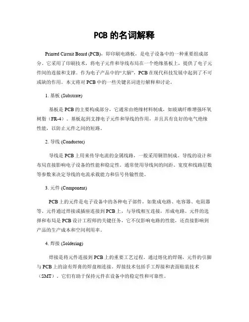
50 PCB常用名词解释 1
- 格式:ppt
- 大小:250.00 KB
- 文档页数:81
PCB的名词解释Printed Circuit Board (PCB),即印刷电路板,是电子设备中的一种重要组成部分。
它采用了印刷技术,将电子元件和导线布局在一个绝缘基板上,提供了电子元件间的连接和支撑。
作为电子产品中的“大脑”,PCB在现代科技发展中起到了不可或缺的作用。
本文将对PCB中的一些关键名词进行解释和讨论。
1. 基板 (Substrate)基板是PCB的主要构成部分,它通常由绝缘材料制成,如玻璃纤维增强环氧树脂(FR-4)。
基板起到支撑电子元件和导线的作用,并且具有良好的电气绝缘性能,以防止元件之间的短路。
2. 导线 (Conductor)导线是PCB上用来传导电流的金属线路,一般采用铜箔制成。
导线的设计和布局直接影响电子设备的性能和稳定性。
通常使用导线间的间距、宽度和线路层数等参数来决定导线的电流承载能力和信号传输性能。
3. 元件 (Component)PCB上的元件是电子设备中的各种电子部件,如集成电路、电容器、电阻器等。
元件通过焊接或插座连接到PCB上,与导线相互连接,形成电路。
元件的选择和布局是PCB设计工程师的关键任务,它不仅影响电路的性能,还直接影响到产品的生产成本和空间利用率。
4. 焊接 (Soldering)焊接是将元件连接到PCB上的重要工艺过程。
通过熔化的焊锡,元件的引脚与PCB上的涂有焊膏的焊盘相连接。
焊接技术包括手工焊接和表面贴装技术(SMT)。
它们有助于保持元件在设备中的稳定性和可靠性。
5. 系统集成 (System Integration)系统集成是指将多个PCB组装在一起,通过元件之间的连接和互联,构成复杂的电子系统。
系统集成是现代电子设备制造的重要环节,它不仅要求PCB间的准确布局和可靠连接,还需要满足信号传输的要求和整体性能的优化。
6. PCB设计 (PCB Design)PCB设计是制定PCB布局、连线和元件安装的过程。
在PCB设计中,设计工程师需要根据电路原理图、电气要求和尺寸限制,合理布局元件和导线。
第三讲PCB术语1、印制电路:在绝缘基材上按预定设计形成的印制元件或印制线路以及两者接合的导电图形。
2、印制线路:在绝缘基材上形成的导电图形,用于元器件之间的连接,但不包括印制元件。
3、预浸材料:由纤维增强材料浸渍热固性树脂后固化至B阶的片状材料。
4、B阶树脂:某些热固性树脂反应的中间阶段,加热时能软化,但不会完全熔解或熔融,此时它与某些溶剂接触能溶胀或部分溶解。
5、纵向/ 横向:层压板机械强度较高的方向。
纸、铜箔、塑料薄膜、玻璃布等片状材料的长度方向,与连续生产时前进的方向一致。
6、增强材料:加入塑料中能使塑料制品的机械强度显著提高的材料,一般为织物或非织物状态的纤维材料。
7、玻璃布:在织布机上将两组互相垂直的玻璃纤维纱交叉编织而成的织物。
8、环氧树脂:含有两个或两个以上环氧基团的,能与多种类型固化剂反应而交联的一类树脂。
9、固化剂:加入树脂中能使树脂聚合而固化的催化剂或反应剂,它是固化树的化学组成部分。
10、阻燃剂:为了止烯显著减小或延缓火焰曼延而加入材料中或涂覆在材料表面的物质。
11、内部识别标志:印在基材表层增强材料上的重复出现的制造厂代号标志,代号字母或数字竖立方向指向增强材料的纵向,阻燃级用红色,非阻燃级用其它色。
12、镀覆孔:孔辟镀覆金属的孔。
同义金属化孔。
13、导通孔:用于印制板不同层中导线之间电气互连的一种镀覆孔。
14、元件孔:将元件引线端固定于印制板并实现电气连接的孔。
15、安装孔:机械安装PCB或机械固定元件于PCB上所使用的孔。
16、孔位:孔中心的的尺寸位置。
17、连接盘(PAD):用于电气连接、元件固定或两者兼备的那部分导电图形。
18、印制插头:靠近印制板边缘,与板边连接器配合的一系列印制接融片。
19、角标:在pcb照相底片图上拐角处的标志。
20、传输线:由导线和绝缘材料组成,具有可控电气特性的载送信号的电路,用于传输高频信号或窄脉冲信号。
21、特性阻抗:传输波中电压与电流的比值,即在传输线的任一点对传输波产生的阻抗。
pcb常用的专业术语PCB常用的专业术语PCB,即印刷电路板,是电子产品中不可或缺的一部分。
在PCB制造过程中,有许多专业术语需要了解。
本文将从材料、工艺、设计等方面介绍PCB常用的专业术语。
一、材料1.基板(Substrate)基板是指印刷电路板上的主体部分,通常由玻璃纤维和树脂复合材料构成。
基板的质量直接影响着整个PCB的性能。
2.铜箔(Copper Foil)铜箔是印刷电路板上最重要的导电层材料,其厚度通常为18um至105um之间。
铜箔的质量和厚度对于PCB的导电性能和可靠性有着重要影响。
3.覆铜板(Copper Clad Board)覆铜板是指在基板表面涂覆一层铜箔而成,通常有单面、双面和多层三种形式。
不同类型的覆铜板适用于不同种类的电路设计需求。
4.阻焊(Solder Mask)阻焊是一种涂在印刷电路板上以保护未焊接区域免受污染和短路的材料。
阻焊通常为绿色、红色或蓝色,具有良好的耐高温性和化学稳定性。
5.沉金(ENIG)沉金是一种表面处理技术,可以在印刷电路板上形成一层金属保护层,提高PCB的可靠性和耐腐蚀性。
沉金通常用于高端PCB产品中。
二、工艺1.蚀刻(Etching)蚀刻是印刷电路板制造中最重要的工艺之一,其目的是去除不需要的铜箔以形成电路图案。
蚀刻过程需要使用化学溶液和光敏树脂等材料。
2.钻孔(Drilling)钻孔是指在印刷电路板上钻洞以安装元器件或连接不同层之间的导线。
钻孔需要使用高速钻头和自动化设备完成。
3.压合(Lamination)压合是指将多个覆铜板通过热压技术粘合在一起形成多层PCB结构。
压合过程需要控制温度、压力和时间等参数,确保PCB质量符合要求。
4.喷锡(Soldering)喷锡是一种表面处理技术,可以在印刷电路板上形成一层锡保护层,提高PCB的可靠性和耐腐蚀性。
喷锡通常用于中端PCB产品中。
5.贴片(SMT)贴片是指将元器件直接安装在印刷电路板上的一种技术。
PCB专业术语大汇集PCB专业术语大汇集PCB是Printed Circuit Board的缩写,即印制电路板。
作为现代电子制造中不可或缺的一个组成部分,PCB技术已经成为电子制造的核心技术之一。
如果你在PCB制造领域工作或学习,那么理解并熟练掌握一些常见的PCB专业术语是非常重要的。
在这篇文章中,我们将罗列一些重要的PCB专业术语和技术名词,以帮助大家更好地理解PCB的制造和设计。
一、PCB制造基础1. PAD:焊盘,指印制电路板上用于焊接元器件的金属区域。
2. VIA:通孔,指在印制电路板上打开的金属通孔,连接不同层之间的电路。
3. Solder mask:焊膜,是一种覆盖在PCB表面的保护层,用于防止无意中的短路和腐蚀。
4. Silk screen:丝印,是印刷在印制电路板上的文字和图像,用于标记焊点、元器件和引脚等信息。
5. Cooper:铜箔,是一种用于制造PCB的材料。
6. Substrate:衬底,指PCB中负责固定和支撑电路的材料。
7. Copper weight:铜厚度,指PCB上铜箔的厚度,单位是oz。
8. Panel:板子,指PCB制造中一组连续的PCB,通常需要在单个板子上打印多个电路。
9. Plating:镀,指将金属材料沉积在印制电路板表面或内部的过程。
10. Tolerance:公差,指PCB制造和设计中可以接受的误差范围。
二、PCB设计技术1. Trace:走线,指印制电路板上的导线,用于连接不同的元器件和电路板上的不同部分。
2. Clearance:间隙,指PCB上不同元器件或电路之间的距离。
3. Net:网络,指一个电路的连接点集合,通常用来描述PCB上的一组连通电路。
4. Gerber:杰伯,是一种文件格式,通常用于将PCB设计转化为PCB生产所需的制造文件。
5. Footprint:插件,指印制电路板上元器件焊盘的设计,用于确保元器件和焊盘正确对齐和正确连接。
pcb专业术语英文及翻译摘要:本文介绍了PCB(Printed Circuit Board,印刷电路板)专业术语的英文表达和翻译,根据内容实际需求分为三大类:PCB制造术语、PCB组装术语和PCB测试术语。
在每个类别下,将列举相关术语及其英文表达和翻译,从而帮助读者更好地理解和运用PCB专业术语。
正文:I. PCB制造术语1. 单、双面板 (Single-sided, Double-sided board)单面板:一种仅在板的一侧进行布线和元件安装的印刷电路板。
双面板:一种在两侧布线和元件安装的印刷电路板。
2. 环氧树脂 (Epoxy Resin)环氧树脂是一种常用的PCB基材,具有良好的绝缘性和耐热性。
3. 铜盖膜 (Copper Foil)铜盖膜是覆盖在印刷电路板表面的一层铜箔,用于电气连接。
4. 阻焊层 (Solder Mask Layer)阻焊层是一种覆盖在印刷电路板表面的保护层,用于防止元件的误焊。
5. 玻璃纤维布 (Glass Fiber Cloth)玻璃纤维布是PCB制造中一种常用的增强材料,用于提高印刷电路板的强度和耐磨性。
6. 焊盘 (Pad)焊盘是印刷电路板上用于连接元件引脚的焊接区域。
7. 过孔 (Through-hole)过孔是印刷电路板上贯穿两侧的孔洞,用于连接不同电子元器件。
8. 排针 (Pin Header)排针是一种插针式连接器,常用于将PCB与其他设备连接。
9. 焊接 (Soldering)焊接是将电子元件与印刷电路板焊接在一起的一种连接方法。
II. PCB组装术语1. 表面贴装技术 (Surface Mount Technology, SMT)表面贴装技术是一种将电子元件直接焊接在印刷电路板表面的组装方法。
2. 波峰焊接 (Wave Soldering)波峰焊接是一种通过将印刷电路板浸入焊锡浪涌中来实现电子元件的连接。
3. 焊接膏 (Solder Paste)焊接膏是表面贴装技术中使用的一种黏性材料,用于在印刷电路板上确定元件的位置并进行焊接。

SMT与PCB术语汇总(2011-01-06 15:08:55)转载标签:分类:软件无线电孔壁线路板多层板教育SMT术语详解AAccelerate Aging ——加速老化,使用人工的方法,加速正常的老化过程。
Acceptance Quality Level (AQL) ——一批产品中最大可以接受的缺陷数目,通常用于抽样计划。
Acceptance Test ——用来测定产品可以接受的试验,由客户与供应商之间决定。
Access Hole ——在多层板连续层上的一系列孔,这些孔中心在同一个位置,而且通到线路板的一个表面。
Annular Ring ——是指保围孔周围的导体部分。
Artwork ——用于生产“Artwork Master”“production Master”,有精确比例的菲林。
Artwork Master ——通常是有精确比例的菲林,其按1:1的图案用于生产“Production Master”。
返回顶部BBack Light ——背光法,是一种检查通孔铜壁完好与否得放大目检方法,其做法是将孔壁外的基材自某一方向上小心的予以磨薄,再利用树脂半透明的原理,从背后射入光线。
假如化学铜孔壁品质完好而无任何破洞或针孔时,则该铜层必能阻绝光线而在显微中呈现黑暗,一旦铜壁有破洞时,则必有光点出现而被观察到,并可放大摄影存证,称为背光法,但只能看到半个孔。
Base Material ——绝缘材料,线路在上面形成。
(可以是刚性或柔性,或两者综合。
它可以是不导电的或绝缘的金属板。
)。
Base Material thickness ——不包括铜箔层或镀层的基材的厚度。
Bland Via ——导通孔仅延伸到线路板的一个表面。
Blister ——离层的一种形式,它是在基材的两层之间或基材与铜箔之间或保护层之间局部的隆起。
Board thickness 是——指包括基材和所有在上面形成导电层在内的总厚度。
Bonding Layer ——结合层,指多层板之胶片层。
p c b最常用术语A/W (artwork) 底片Ablation 烧溶(laser),切除abrade 粗化abrasion resistance 耐磨性absorption 吸收ACC ( accept ) 允收accelerated corrosion test 加速腐蚀accelerated test 加速试验acceleration 速化反应accelerator 加速剂acceptable 允收activator 活化液active work in process 实际在制品adhesion 附着力adhesive method 黏着法air inclusion 气泡air knife 风刀amorphous change 不定形的改变amount 总量amylnitrite 硝基戊烷analyzer 分析仪annular ring 环状垫圈;孔环anode slime (sludge) 阳极泥anodizing 阳极处理AOI ( automatic optical inspection ) 自动:光学检测applicable documents 引用之文件AQL sampling 允收水准抽样aqueous photoresist 液态光阻aspect ratio 纵横比(厚宽比)As received 到货时back lighting 背光back-up 垫板banked work in process 预留在制品base material 基材baseline performance 基准绩效batch 批beta backscattering 贝他射线照射法beveling 切斜边;斜边biaxial deformation 二方向之变形black-oxide 黑化blank controller 空白对照组blank panel 空板blanking 挖空blip 弹开blister 气泡;起泡blistering 气泡blow hole 吹孔board-thickness error 板厚错误bonding plies 黏结层bow ; bowing 板弯break out 从平环内破出bridging 搭桥;桥接BTO (Build To Order) 接单生产burning 烧焦burr 毛边(毛头)camcorder 一体型摄录放机carbide 碳化物carlson pin 定位梢carrier 载运剂catalyzing 催化catholic sputtering 阴极溅射法caul plate 隔板;钢板calibration system requirements 校验系统之各种要求center beam method 中心光束法central projection 集中式投射线certification 认证chamfer 倒角(金手指)chamfering 切斜边;倒角characteristic impedance 特性阻抗charge transfer overpotential 电量传递过电压chase 网框checkboard 棋盘chelator 蟹和剂chemical bond 化学键chemical vapor deposition 化学蒸着镀circumferential void 圆周性之孔破clad metal 包夹金属clean room 无尘室clearance 间隙coat 镀外表coating error 防焊覆盖错误coefficient of thermal expansion (CTE) 热澎胀系数cold solder joint 冷焊点cold-weld 金属粉末冷焊color 颜色color error 颜色错误compensation 补偿competitive performance 竞争力绩效complex salt 错化物complexor 错化物component hole 零件孔component side 零件面concentric 同心conformance 密贴性consumer products 消费性产品contact resistance 接触电阻continuous performance 连续发挥效能contract service 协力厂controlled split 均裂式conventional flow 乱流方式conventional tensile test 传统张力测试法conversion coating 转化层convex 突出coordinate list 数据清单copper claded laminates (CCL) 铜箔基板copper exposure 线路露铜copper mirror 镜铜copper pad 铜箔圆配copper residue (copper splash) 铜渣corrosion rate numbering 腐蚀速率计数系统corrosion resistance 抗蚀性coulombs law 库伦定律countersink 喇叭孔coupon 试样coupon location 试样点covering power 遮盖力CPU 中央处理器crack 破裂;裂痕crazing 裂痕;白斑cross linking 交联聚合cross talk 呼应作用crosslinking 交联crystal collection 结晶收集curing 聚合体current efficiency 电流效率cut-outs 挖空cutting 裁板cyanide 氰化物cycles of learning 学习循环cycle-time reduction 交期缩短date code 周期deburring 去毛头dedicated 专用型degradation 退变delamination 分层dent / pin hole 凹陷/ 针孔department of defense 国防部designation 字码简示法de-smear 除胶渣developing 显影dewetting 缩锡dewetting time 缩锡时间dimension error 外形尺寸错误dielectric constant 介质常数difficulty 困难度difunctional 双功能dimension 尺寸dimension stability 尺寸安定性dimensional stability 尺度安定性dimension and tolerance 尺寸与公差dirty hole 孔内异物discolor hole 孔黑;孔灰;氧化discoloration 变色disposable eyelet method 消耗性铆钉法distortion factor 尺寸变形函数double side 双面板downtime 停机时间drill 钻孔drill bit 钻头drill facet 钻尖切萷面drill pointer 钻尖重(研)磨机drilled blank board 已钻孔之裸板drilling 钻孔dry film 干膜ductility 延展性economy of scale 经济规模edge spacing 板边空地edge-board contact ( gold finger ) 金手指efficiency 能量效率electric test 电测electrical testing 电测;测试electrochemical machine ECM 电化学加工法electrochemical reactor 电化学反应器electroforming 电铸electroless plate 化学铜electroless-deposition 无电镀electropolishing 电解拋光electrorefining 电解精炼electrowinning 电解萃取elliptical set 椭圆形embrittlement 脆性entitlement performance 可达成绩效entrapment 电镀夹杂物epoxy 环氧树酯equipotential 电位线error data file 异常情形etch rate 蚀铜速率etchants 蚀刻液etchback 回蚀evaluation program 评估用程序exposure 曝光external pin method 外部插梢法eyelet hole 铆钉孔Eyeletting 铆眼fabric 网布failure 故障fast response 快速响应fault 瑕庛;缺陷fiber exposure 纤维显露fiber protrusion 纤维突出fiducial mark 光学点,基准记号filler 填充料film 底片filtration 过滤finished board 成品fixing 固着fixture 电测夹具(治具)flaking off 粹离flammability rating 燃性等级flare 喇叭形孔flat cable 并排电缆feedback loop 回馈循环first-in-first-out (FIFO) 先进先出flexible manufacturing system (FMS) 弹性制造系统flux 助焊剂foil distortion 铜层变形fold 空泡foreign include 异物foreign material 基材内异物free radical chain polymerization 自由基连锁聚合fully additive 加成法fully annealed type 彻底回火轫化之类形function 函数fundamental and basic 基本fungus resistance 抗霉性funnel flange 喇叭形折翼galvanized 加法尼化制程gap 钻尖分开gauge length 有效长度gel time 胶化时间general resist ink 一般阻剂油墨general 通论general industrial 一般性(电子)工业级geometrical levelling 几何平整glass transition temperature (Tg) 玻璃态转换温度Gold 金gold finger 金手指gold plating 镀金golden board 标准板gouges 刷磨凹沟gouging 挖破grain boundary 金属晶体之四边green 绿色grip 夹头ground plane 接地层ground plane clearance 接地空环hackers 骇客HAL ( hot air leveling ) 喷锡haloing 白边;白圈hardener 硬化剂hardness 硬度hepa filter 空气滤清器high performance industrial 高性能(电子)工业级high reliability 高可靠度high resolution 高分辨率high temperature elongation (HTE) 高温延展性铜箔high temperature epoxy (HTE) 高温树酯hit 击hole counter 数孔机hole diameter 孔径hole diameter error 孔径错误hole location 孔位hole number 孔数hole wall quality 孔壁品质hook 外弧hot dip 热浸法hull cell 哈氏槽hybrid 混成集成电路hydrogen bonding 氢键hydrolysis 水解hydrometallurgy 湿法冶金法image analysis system 影像分析系统image transfer 影像转移immersion gold 浸金(化镍金)immersion plating 浸镀法impedance 阻抗infrared reflow 红外线重熔inhibitor 热聚合抑制剂injection mold 射模ink 油墨innerlayer & outlayer 内外层insulation resistance 绝缘电阻intended position 应该在的位置intensifier 增强器intensity 强度inter molecular exchange 交互改变interconnection 互相连通ionic contaminants 离子性污染物ionic contamination testing 离子污染试验IPA 异丙醇5I : inspiration (启蒙)identification 确认计划目标implementation 改善方案information 数据internalization 制度化invisible inventory 无形的库存knife edges 刀缘Knoop 努普(硬度单位)kraft paper 牛皮纸返回顶部laminar flow 层流laminate 基层板laminating 压合lamination 压合laminator 压膜机land 焊垫lay back 刃角磨损lay up 组合叠板layout 布线;布局lead screw 牵引螺丝leakage 漏电learning curve 学习曲线legend 文字标记leveling 平整levelling additive 平整剂levelling power 平整力life support 维系生命limiting current 极限电流line space 线距line width 线宽linear variable differential transformer(LVDL) 线性可变差动:转换器liquid 液状(态)liquid crystal resins 液晶树脂liquid photoimageable solder resist ink 液态感光防焊油墨liquid photoresist ink 液态光阻剂油墨lot size 批量lower carrier 底部承载板mechanical plating 机祴镀法machine scrub 刷磨清洁法macrothrowing power 巨分布力margin 钻头刃带market share 市场占有率marking error 文字错误masked leveling 儰装平整mass lamination 大型压板mass transfer 质量传送效应mass transfer overpotential 质量传递过电压mass transportation 质传master drawing 主图;蓝图material use factor 材料使用率mealing 泡点;白点memory 记忆装置meniscograph solderability measurement 新月型焊锡效果microetch 微蚀microetching 微蚀microfocus 微焦距microfocus system 微焦距系统microprofile 微表面microsectioning 微切片法microthrowing power 微分布力migration 迁移mini-tensile tester 迷你拉力测试仪mis hole location 孔位错误misregistration 焊锡面与零件面对位偏差misregsitration 对不准moisture and insulation resistance test 湿气与绝缘电阻试验molded circuit board (MCB) 模制电路板monoethanal amine 单乙醇氨monohydrate state 水化物monomer 单分子膜;单体mouse bite 锯齿;蚀刻缺口msec 毫秒muffle furnace 高温焚火炉multichip 超大IC型(多芯片模块) mylar 保护膜nail head 钉头NC drill 数字钻孔机negative etchback 反回蚀negative film 负片negative rake angle 负抠耙角network 回路;网络neutralization 中和nick 缺口nickel 镍nodule 铜瘤;瘤粒no flow resin 不流树脂noise 噪声nominal 标示nominal dimension 标定长度nominal gel time 标示胶性时间nominal resin content 标示胶含量nominal resin flow 标示胶流量nominal scaled flow thickness 标示比例流量厚度OA equip 办公室自动:化设备obsolescence factor 报废因素OEM 原设备制造商offset-list 补偿数据清单ohmmeter 欧姆计open 断路open circuits 断路open short testing 断短路测试opening 开口original art work (A/W) 原稿底片Others 其它outgrowth 增出over design 牛刀杀鸡overlap 钻尖重叠overlay entry 盖板overpotential 过电压oxidation 氧化oxide treatment 黑化处理oxided cytochrome 氧化性之细包色素oxygen evolution 氧气发生反应packed bed 充填床式pad 锡垫;圆配pad copper exposure pad露铜panel 小型板面;母板panel plating 一次铜电镀parasitic 寄生的part no. 料号pattern plating 二次铜电镀PCB ( print circuit board ) 印刷电路板pcs 片peel strength 抗撕强度peeling off 剥离(剥落)performance specification 性能规范permittivity 透电率perspectives on experience 经验透视PET 聚酯photodiode detector 发光二极管侦测器photo initiator 感光启始剂photoresist 光阻phototool 光具(指工作底片)piece 子板面pinceton applied research 腐蚀测定仪pink ring 粉红圈pit 凹点pitch 脚距planar 平面plating 电镀plating exposure 下镀层露出plug gauge 插规plug hole 孔塞PNL (panel) 排板polar-polar interaction 极性之间的吸力polyester 聚酯类polyglycols 聚乙二醇polyimide 聚亚醯氨poor bevelling 磨边加工引起突起,剥离poor drill 孔形不良poor HAL 喷锡不良poor marking 字体不良poor pad 锡垫不良poor printed 印刷偏差poor solderability 焊锡性不良poor touch-up 补线不良position control system 位置控制系统positive rake angle 正抠耙角power curve model 幕次曲线模式practice 工艺惯例preferred 良好premature tearing 提前撕裂prepolymer 预聚合物prepreg 胶片pre-process ( front-end) 制前press 压床press cycle 压合周期primary current distribution 一次电流分布primary 主要product lifetimes 生命周期product process 制程promoter 促进剂protocal 初步资料prussic acid 普鲁士酸PTF-based process 厚膜糊法PTH (plating though hole) 导通孔pull away 拉开pumice 浮石粉pumice scrub 喷砂清洁法pyrometallurgy 火烧法冶炼QC ( quality control) 品管QFP (quad flat pack ) 扁方型封装体qualification inspection 资格审查检验qualification testing 资格检定quality classification 品质等级quantitative 计量式测试rack 挂架radiometer 能量剂rake angle 抠耙角RAM [Random Access Memory 随机存取内存real time 关键时刻recessed trace process 凹槽线路法recovery tank 回收槽reduction 还原re-eninforcement 强化refraction 折光率reinforcement style 补强材料的型式register mark 对位用标记registration hole 对位孔registration pattern 长方形铜地REJ ( reject ) 退货;拒收rejectable 拒收release agent 脱模剂relief angle 浮离角remark 备注repair 修理resin content 树脂含量(胶含量)resin flow 胶流量resin flow percentage 树脂流量之百分率resin recession 树脂下陷resin smear 胶渣resist strippers 剥干膜剂resistor network 排列电阻resolution 解像度return on assets 资产报酬率reversibility 可逆性rework 重工rosin 天然松香rotating cylinder 旋转圆柱形roughtness 孔壁粗糙;粗慥routing 切外形,成型routing bit 铣刀runout 偏转S/L on hole 孔内沾文字S/M ( solder mask ), S/L 防焊文字S/M (solder mask) 防焊S/M error 防焊种类错误S/M on hole 孔内绿漆salt spray test 盐水喷雾试验sampling size 抽样数scope 范围scored 刻痕scoring 枢槽;刮线scrap 废框scratches 刮伤screen printing 网版印刷scum 透明残膜sealing 封孔处理secondary 次要semi-additive 半加成法sensitize 敏化sensitizer 敏化液separator 钢隔板sequential lamination 渐成式压法serrated edges 毛边shatter 破碎short 短路shunt 分路silane treatment 硅烷处理silicone coupling agent 硅烷偶合剂silk screen 文字印刷simulator 仿真器single axis 单轴sizing 底片之伸缩补偿skip 漏印skip printing 跳印;漏印sliver 丝条slot 开槽slotting 开槽SMD ( surface mount device ) 表面黏着组件smear 胶渣SMT ( surface mount technology )表面黏着技术sodium carbonate monohydrate 结晶水碳酸钠soft tooling 软性工具solder 焊锡; 锡铅solder bridge 锡桥solder bump 锡突solder float 漂锡solder mask adhesion 绿漆附着力solder on G/F 金手指沾锡solder on trace 线路沾锡solder plug 锡塞solder side 焊锡面solderability 焊锡性solid carbide 实质碳化物spacing 间距spacing nonenough 间距不足SPC ( Statistical Process Control ) 统计生管specification 规范special considerations 特别考虑spin coating 旋转涂布spindle 钻轴spiral contractometer 螺旋收缩仪spot face 铣靶spray coating 喷涂Squeegee 刮刀stacking structure 叠板结构stamping 冲压standard hydraulic lamination标准液压法standardizing 标准化starvation 缺胶step tablet 格片数stock option 认股选择权strain 应度strength 强度stressmeter 应力计subtractive 减除法surface convex 表面突起surface examination 表面检查surface insulation resistance (SIR) 表面绝缘电阻surface mount 表面黏着方式surface roughness 表面粗慥度surges 突波switch circuit 开关线路tab 金手指tack free 不黏taped hole gauge 锥形孔规target hole 靶孔task force 任务编组tensile strength 抗拉强度tensile stress 张性应力tent 浮盖terms and definitions 术语与定义termination load 抗匹配负载test circuit 测试线路test method 试验方法test point 测试点thermal shock 热震荡试验thermal stress 热应力试验thermistor 热电感应式thermo cycling 热循环试验theoretical cycle time 理论性周期时间thickness 厚度time to market 上市时机thickness distribution 厚度分布thief 补助阴极thin core 薄基板;内层板throwing power 分布力tolerance 公差;容差tooling hole 工具孔torque load 扭力拒之负载total quality program 全面的品质计划toughness 坚度trace error 线路错误trace nick & pin hole 线路缺口及针孔trace peeling 线路剥离trace pin-hole 线路针孔trace surface roughness 线路表面粗糙tarnish and oxide resist 抗污抗氧化剂transmittance 透光度trim line 裁切线true levelling 真平整true position 真正位置的孔;真位twist 板翘type 种类umbra 本影undercut 侧蚀uneven coating 喷锡厚镀不平整universal 万用型universal tensile tester 万用拉力试验机universal tester 泛用型测试机upper carrier 顶部承载钢uptime 稼动:时间vacuum deposition 真空蒸镀法vacuum hydraulic lamination真空液压法vaporizer 气化室V-cut V形槽vertical microsection 垂直微切片via hole 导通孔visible inventory 有形的库存vision inspection 目视检查Void 孔破void in hole 孔壁上的破洞void in PTH hole 孔破walkman 随身听warehouse 仓库warp 板弯warp , warpage 板弯water absorption 吸水性wear resistance 耐磨度weave exposure 纤纹显露weave texture 织纹隐现wedge angle 契尖角week 周wet chemistry 湿式化学制程wet film 湿膜wet lamination 湿膜压膜法wet process 湿制程wetting 沾锡wetting balance 沾锡平衡法wicking 渗铜;渗入;灯蕊效应width 宽度width reduce 线细width-to-thickness ratio 宽度与厚度的比值window 操作范围work-in-process 在制品work order 工单working film 工作片working master 工作母片year 年yellow 金黄色yield 良率。
PCB术语PCB线路设计及制前作业术语1、Annular Ring 孔环指绕接通孔壁外平贴在板面上的铜环而言。
在内层板上此孔环常以十字桥与外面大地相连,且更常当成线路的端点或过站。
在外层板上除了当成线路的过站之外,也可当成零件脚插焊用的焊垫。
与此字同义的尚有 Pad(配圈)、 Land (独立点)等。
2、Artwork 底片在电路板工业中,此字常指的是黑白底片而言。
至于棕色的“偶氮片”(Diazo Film)则另用 Phototool 以名之。
PCB 所用的底片可分为“原始底片”Master Artwork 以及翻照后的“工作底片”Working Artwork 等。
3、Basic Grid 基本方格指电路板在设计时,其导体布局定位所着落的纵横格子。
早期的格距为 100 mil,目前由于细线密线的盛行,基本格距已再缩小到 50 mil。
4、Blind Via Hole 盲导孔指复杂的多层板中,部份导通孔因只需某几层之互连,故刻意不完全钻透,若其中有一孔口是连接在外层板的孔环上,这种如杯状死胡同的特殊孔,称之为“盲孔”(Blind Hole)。
5、Block Diagram 电路系统块图将组装板及所需的各种零组件,在设计图上以正方或长方形的空框加以框出,且用各种电性符号,对其各框的关系逐一联络,使组成有系统的架构图。
6、Bomb Sight 弹标原指轰炸机投弹的瞄准幕。
PCB 在底片制作时,为对准起见也在各角落设置这种上下两层对准用的靶标,其更精确之正式名称应叫做Photographers' Target。
7、Break-away panel 可断开板指许多面积较小的电路板,为了在下游装配线上的插件、放件、焊接等作业的方便起见,在 PCB 制程中,特将之并合在一个大板上,以进行各种加工。
完工时再以跳刀方式,在各独立小板之间进行局部切外形(Routing)断开,但却保留足够强度的数枚“连片”(Tie Bar 或Break-away Tab),且在连片与板边间再连钻几个小孔;或上下各切 V 形槽口,以利组装制程完毕后,还能将各板折断分开。
PCB專業英譯術語一、綜合辭彙1、印製電路:printed circuit2、印製線路:printed wiring3、印製板:printed board4、印製板電路:printed circuit board (PCB)5、印製線路板:printed wiring board(PWB)6、印製元件:printed component7、印製接點:printed contact8、印製板裝配:printed board assembly9、板:board10、單面印製板:single-sided printed board(SSB)11、雙面印製板:double-sided printed board(DSB)12、多層印製板:mulitlayer printed board(MLB)13、多層印製電路板:mulitlayer printed circuit board14、多層印製線路板:mulitlayer prited wiring board15、剛性印製板:rigid printed board16、剛性單面印製板:rigid single-sided printed borad17、剛性雙面印製板:rigid double-sided printed borad18、剛性多層印製板:rigid multilayer printed board19、撓性多層印製板:flexible multilayer printed board20、撓性印製板:flexible printed board21、撓性單面印製板:flexible single-sided printed board22、撓性雙面印製板:flexible double-sided printed board23、撓性印製電路:flexible printed circuit (FPC)24、撓性印製線路:flexible printed wiring25、剛性印製板:flex-rigid printed board, rigid-flex printed board26、剛性雙面印製板:flex-rigid double-sided printed board, rigid-flex double-sided printed27、剛性多層印製板:flex-rigid multilayer printed board, rigid-flex multilayer printed board28、齊平印製板:flush printed board29、金屬芯印製板:metal core printed board30、金屬基印製板:metal base printed board31、多重佈線印製板:mulit-wiring printed board32、陶瓷印製板:ceramic substrate printed board33、導電膠印制板:electroconductive paste printed board34、模塑電路板:molded circuit board35、模壓印製板:stamped printed wiring board36、順序層壓多層印製板:sequentially-laminated mulitlayer37、散線印製板:discrete wiring board38、微線印製板:micro wire board39、積層印製板:buile-up printed board40、積層多層印製板:build-up mulitlayer printed board (BUM)41、積層撓印製板:build-up flexible printed board42、表面層合電路板:surface laminar circuit (SLC)43、埋入凸塊連印製板:B2it printed board44、多層膜基板:multi-layered film substrate(MFS)45、層間全內導通多層印製板:ALIVH multilayer printed board46、載晶片板:chip on board (COB)47、埋電阻板:buried resistance board48、母板:mother board49、子板:daughter board50、背板:backplane51、裸板:bare board52、鍵盤板夾心板:copper-invar-copper board53、動態撓性板:dynamic flex board54、靜態撓性板:static flex board55、可斷拼板:break-away planel56、電纜:cable57、撓性扁平電纜:flexible flat cable (FFC)58、薄膜開關:membrane switch59、混合電路:hybrid circuit60、厚膜:thick film61、厚膜電路:thick film circuit62、薄膜:thin film63、薄膜混合電路:thin film hybrid circuit64、互連:interconnection65、導線:conductor trace line66、齊平導線:flush conductor67、傳輸線:transmission line68、跨交:crossover69、板邊插頭:edge-board contact70、增強板:stiffener71、基底:substrate72、基板面:real estate73、導線面:conductor side74、元件面:component side75、焊接面:solder side76、印製:printing77、網格:grid78、圖形:pattern79、導電圖形:conductive pattern80、非導電圖形:non-conductive pattern81、字元:legend82、標誌:mark[/size]作者:ilww 2004-11-10 16:18:00)二、基材:1、基材:base material2、層壓板:laminate3、覆金屬箔基材:metal-clad bade material4、覆銅箔層壓板:copper-clad laminate (CCL)5、單面覆銅箔層壓板:single-sided copper-clad laminate6、雙面覆銅箔層壓板:double-sided copper-clad laminate7、複合層壓板:composite laminate8、薄層壓板:thin laminate9、金屬芯覆銅箔層壓板:metal core copper-clad laminate10、金屬基覆銅層壓板:metal base copper-clad laminate11、撓性覆銅箔絕緣薄膜:flexible copper-clad dielectric film12、基體材料:basis material13、預浸材料:prepreg14、粘結片:bonding sheet15、預浸粘結片:preimpregnated bonding sheer16、環氧玻璃基板:epoxy glass substrate17、加成法用層壓板:laminate for additive process18、預製內層覆箔板:mass lamination panel19、內層芯板:core material20、催化板材:catalyzed board ,coated catalyzed laminate21、塗膠催化層壓板:adhesive-coated catalyzed laminate22、塗膠無催層壓板:adhesive-coated uncatalyzed laminate23、粘結層:bonding layer24、粘結膜:film adhesive25、塗膠粘劑絕緣薄膜:adhesive coated dielectric film26、無支撐膠粘劑膜:unsupported adhesive film27、覆蓋層:cover layer (cover lay)28、增強板材:stiffener material29、銅箔面:copper-clad surface30、去銅箔面:foil removal surface31、層壓板面:unclad laminate surface32、基膜面:base film surface33、膠粘劑面:adhesive faec34、原始光潔面:plate finish35、粗面:matt finish36、縱向:length wise direction37、模向:cross wise direction38、剪切板:cut to size panel39、酚醛紙質覆銅箔板:phenolic cellulose paper copper-clad laminates(phenolic/paper CCL)40、環氧紙質覆銅箔板:epoxide cellulose paper copper-clad laminates (epoxy/paper CCL)41、環氧玻璃布基覆銅箔板:epoxide woven glass fabric copper-clad laminates42、環氧玻璃布紙複合覆銅箔板:epoxide cellulose paper core, glass cloth surfaces copper-clad laminates43、環氧玻璃布玻璃纖維複合覆銅箔板:epoxide non woven/woven glass reinforced copper-clad laminates44、聚酯玻璃布覆銅箔板:ployester woven glass fabric copper-clad laminates45、聚醯亞胺玻璃布覆銅箔板:polyimide woven glass fabric copper-clad laminates46、雙馬來醯亞胺三嗪環氧玻璃布覆銅箔板:bismaleimide/triazine/epoxide woven glass fabric copper-clad lamimates47、環氧合成纖維布覆銅箔板:epoxide synthetic fiber fabric copper-clad laminates48、聚四乙烯玻璃纖維覆銅箔板:teflon/fiber glass copper-clad laminates49、超薄型層壓板:ultra thin laminate50、陶瓷基覆銅箔板:ceramics base copper-clad laminates51、紫外線阻擋型覆銅箔板:UV blocking copper-clad laminates作者:ilww 2004-11-10 16:19:00)三、基材的材料1、A階樹脂:A-stage resin2、B階樹脂:B-stage resin3、C階樹脂:C-stage resin4、環氧樹脂:epoxy resin5、酚醛樹脂:phenolic resin6、聚酯樹脂:polyester resin7、聚醯亞胺樹脂:polyimide resin8、雙馬來醯亞胺三嗪樹脂:bismaleimide-triazine resin9、丙烯酸樹脂:acrylic resin10、三聚氰胺甲醛樹脂:melamine formaldehyde resin11、多官能環氧樹脂:polyfunctional epoxy resin12、溴化環氧樹脂:brominated epoxy resin13、環氧酚醛:epoxy novolac14、氟樹脂:fluroresin15、矽樹脂:silicone resin16、矽烷:silane17、聚合物:polymer18、無定形聚合物:amorphous polymer19、結晶現象:crystalline polamer20、雙晶現象:dimorphism21、共聚物:copolymer22、合成樹脂:synthetic23、熱固性樹脂:thermosetting resin24、熱塑性樹脂:thermoplastic resin25、感光性樹脂:photosensitive resin26、環氧當量:weight per epoxy equivalent (WPE)27、環氧值:epoxy value28、雙氰胺:dicyandiamide29、粘結劑:binder30、膠粘劑:adesive31、固化劑:curing agent32、阻燃劑:flame retardant33、遮光劑:opaquer34、增塑劑:plasticizers35、不飽和聚酯:unsatuiated polyester36、聚酯薄膜:polyester37、聚醯亞胺薄膜:polyimide film (PI)38、聚四氟乙烯:polytetrafluoetylene (PTFE)39、聚全氟乙烯丙烯薄膜:perfluorinated ethylene-propylene copolymer film (FEP)40、增強材料:reinforcing material41、玻璃纖維:glass fiber42、E玻璃纖維:E-glass fibre43、D玻璃纖維:D-glass fibre44、S玻璃纖維:S-glass fibre45、玻璃布:glass fabric46、非織布:non-woven fabric47、玻璃纖維墊:glass mats48、紗線:yarn49、單絲:filament50、絞股:strand51、緯紗:weft yarn52、經紗:warp yarn53、但尼爾:denier54、經向:warp-wise55、緯向:weft-wise, filling-wise56、織物經緯密度:thread count57、織物組織:weave structure58、平紋組織:plain structure59、壞布:grey fabric60、稀鬆織物:woven scrim61、弓緯:bow of weave62、斷經:end missing63、缺緯:mis-picks64、緯斜:bias65、折痕:crease66、雲織:waviness67、魚眼:fish eye68、毛圈長:feather length69、厚薄段:mark70、裂縫:split71、撚度:twist of yarn72、浸潤劑含量:size content73、浸潤劑殘留量:size residue74、處理劑含量:finish level75、浸潤劑:size76、偶聯劑:couplint agent77、處理織物:finished fabric78、聚醯胺纖維:polyarmide fiber79、聚酯纖維非織布:non-woven polyester fabric80、浸漬絕緣縱紙:impregnating insulation paper81、聚芳醯胺纖維紙:aromatic polyamide paper82、斷裂長:breaking length83、吸水高度:height of capillary rise84、濕強度保留率:wet strength retention85、白度:whitenness86、陶瓷:ceramics87、導電箔:conductive foil88、銅箔:copper foil89、電解銅箔:electrodeposited copper foil (ED copper foil)90、壓延銅箔:rolled copper foil91、退火銅箔:annealed copper foil92、壓延退火銅箔:rolled annealed copper foil (RA copper foil)93、薄銅箔:thin copper foil94、塗膠銅箔:adhesive coated foil95、塗膠脂銅箔:resin coated copper foil (RCC)96、複合金屬箔:composite metallic material97、載體箔:carrier foil98、殷瓦:invar99、箔(剖面)輪廓:foil profile100、光面:shiny side101、粗糙面:matte side102、處理面:treated side103、防銹處理:stain proofing104、雙面處理銅箔:double treated foil四、設計1、原理圖:shematic diagram2、邏輯圖:logic diagram3、印製線路佈設:printed wire layout4、佈設總圖:master drawing5、可製造性設計:design-for-manufacturability6、電腦輔助設計:computer-aided design.(CAD)7、電腦輔助製造:computer-aided manufacturing.(CAM)8、電腦集成製造:computer integrat manufacturing.(CIM)9、電腦輔助工程:computer-aided engineering.(CAE)10、電腦輔助測試:computer-aided test.(CAT)11、電子設計自動化:electric design automation .(EDA)12、工程設計自動化:engineering design automaton .(EDA2)13、組裝設計自動化:assembly aided architectural design. (AAAD)14、電腦輔助製圖:computer aided drawing15、電腦控制顯示:computer controlled display .(CCD)16、佈局:placement17、佈線:routing18、布圖設計:layout19、重布:rerouting20、模擬:simulation21、邏輯類比:logic simulation22、電路類比:circit simulation23、時序模擬:timing simulation24、模組化:modularization25、佈線完成率:layout effeciency26、機器描述格式:machine descriptionm format .(MDF)27、機器描述格式資料庫:MDF databse28、設計資料庫:design database29、設計原點:design origin30、優化(設計):optimization (design)31、供設計優化坐標軸:predominant axis32、表格原點:table origin33、鏡像:mirroring34、驅動文件:drive file35、中間檔:intermediate file36、製造檔:manufacturing documentation37、佇列支撐資料庫:queue support database38、元件安置:component positioning39、圖形顯示:graphics dispaly40、比例因數:scaling factor41、掃描填充:scan filling42、矩形填充:rectangle filling43、填充域:region filling44、實體設計:physical design45、邏輯設計:logic design46、邏輯電路:logic circuit47、層次設計:hierarchical design48、自頂向下設計:top-down design49、自底向上設計:bottom-up design50、線網:net51、數位化:digitzing52、設計規則檢查:design rule checking53、走(布)線器:router (CAD)54、網路表:net list55、電腦輔助電路分析:computer-aided circuit analysis56、子線網:subnet57、目標函數:objective function58、設計後處理:post design processing (PDP)59、互動式製圖設計:interactive drawing design60、費用矩陣:cost metrix61、工程圖:engineering drawing62、方塊框圖:block diagram63、迷宮:moze64、元件密度:component density65、巡迴售貨員問題:traveling salesman problem66、自由度:degrees freedom67、入度:out going degree68、出度:incoming degree69、曼哈頓距離:manhatton distance70、歐幾裏德距離:euclidean distance71、網路:network72、陣列:array73、段:segment74、邏輯:logic75、邏輯設計自動化:logic design automation76、分線:separated time77、分層:separated layer78、定順序:definite sequenc作者:ilww 2004-11-10 16:21:00)五、形狀與尺寸:1、導線(通道):conduction (track)2、導線(體)寬度:conductor width3、導線距離:conductor spacing4、導線層:conductor layer5、導線寬度/間距:conductor line/space6、第一導線層:conductor layer No.17、圓形盤:round pad8、方形盤:square pad9、菱形盤:diamond pad10、長方形焊盤:oblong pad11、子彈形盤:bullet pad12、淚滴盤:teardrop pad13、雪人盤:snowman pad14、V形盤:V-shaped pad15、環形盤:annular pad16、非圓形盤:non-circular pad17、隔離盤:isolation pad18、非功能連接盤:monfunctional pad19、偏置連接盤:offset land20、腹(背)裸盤:back-bard land21、盤址:anchoring spaur22、連接盤圖形:land pattern23、連接盤網格陣列:land grid array24、孔環:annular ring25、元件孔:component hole26、安裝孔:mounting hole27、支撐孔:supported hole28、非支撐孔:unsupported hole29、導通孔:via30、鍍通孔:plated through hole (PTH)31、余隙孔:access hole32、盲孔:blind via (hole)33、埋孔:buried via hole34、埋/盲孔:buried /blind via35、任意層內部導通孔:any layer inner via hole (ALIVH)36、全部鑽孔:all drilled hole37、定位孔:toaling hole38、無連接盤孔:landless hole39、中間孔:interstitial hole40、無連接盤導通孔:landless via hole41、引導孔:pilot hole42、端接全隙孔:terminal clearomee hole43、准表面間鍍覆孔:quasi-interfacing plated-through hole44、准尺寸孔:dimensioned hole45、在連接盤中導通孔:via-in-pad46、孔位:hole location47、孔密度:hole density48、孔圖:hole pattern49、鑽孔圖:drill drawing50、裝配圖:assembly drawing51、印製板組裝圖:printed board assembly drawing52、參考基準:datum referan電路板朮語總整理*****A*****Abietic Acid松脂酸.Abrasion Resistance耐磨性.Abrasives磨料,刷材.ABS樹脂.Absorption吸收(入).Ac Impedance交流阻抗.Accelerated Test(Aging)加速老化(試驗). Acceleration速化反應.Accelerator 加速劑,速化劑.Acceptability,Acceptance 允收性,允收.Access Hole露出孔,穿露孔.Accuracy准確度.Acid Number (Acid Value)酸值.Acoustic Microscope (AM)感音成像顯微鏡. Acrylic壓克力(聚丙烯酸樹脂).Actinic Light (or Intensity, or Radiation)有效光. Activation活化.Activator活化劑.Active Carbon活性炭.Active Parts(Devices)主動零件.Acutance解像銳利度.Addition Agent添加劑.Additive Process加成法.Adhesion附著力.Adhesion Promotor附著力促進劑.Adhesive膠類或接著劑.Admittance導納(阻抗的倒數).Aerosol噴霧劑,氣熔膠,氣懸體.Aging老化.Air Inclusion氣泡夾雜.Air Knife風刀.Algorithm演算法.Aliphatic Solvent脂肪族溶劑.Aluminium Nitride(AlN)氮化鋁.Ambient Tamp環境溫度.Amorphous無定形,非晶形.Amp-Hour安培小時.Analog Circuit/Analog Signal類比電路/類比訊號. Anchoring Spurs著力爪.Angle of Contack接觸角.Angle of Attack攻角.Anion陰離子.Anisotropic異向性,單向的.Anneal 韌化(退火).Annular Ring孔環.Anode陽極.Anode Sludge陽極泥.Anodizing陽極化.ANSI美國標準協會.Anti-Foaming Agent消泡劑.Anti-pit Agent抗凹劑.AOI自動光學檢驗.Apertures開口,鋼版開口.AQL品質允收水準.AQL(Acceptable Quality Level)允收品質水準.Aramid Fiber聚醯胺纖維.Arc Resistance耐電弧性.Array排列.Artwork底片.ASIC特定用途勣體電路器.Aspect Ratio縱橫比.Assembly組裝裝配.A-stage A階段.ATE自動電測設備.Attenuation訊號衰減.Autoclave壓力鍋.Axial-lead軸心引腳.Azeotrope共沸混合液.*****B*****Back Light (Back Lighting)背光法.Back Taper反錐斜角.Backpanels, Backplanes支撐板.Back-up 墊板.Balanced Transmission Lines平衡式傳輸線.Ball Grid Array球腳陣列(封裝).Bandability彎曲性.Banking Agent護岸劑.Bare Chip Assembly裸體晶片組裝.Barrel孔壁,滾鍍.Base Material基材.Basic Grid基本方格.Batch批.Baume波美度(凡液體比重比水重則 Be=145-(145÷Sp.Gr) 凡液體比重比水輕則 Be=140÷(Sp.Gr-130)*Sp.Gr 為比重即同體勣物質對"純水"1g/cm的比值). Beam lead光芒式的平行密集引腳.Bed-of-Nail Testing針床測試.Bellows Conact彈片式接觸.Beta Ray Backscatter貝他射線反彈散射. Bevelling切斜邊.Bias斜張綱布,斜纖法.Bi-Level Stencil]雙階式鋼板.Binder粘結劑.Bits頭(Drill Bits).Black Oxide黑氧化層.Blanking沖空斷開.Bleack 漂洗.Bleeding溢流.Blind Via Hole肓通孔.Blister局部性分層或起泡.Block Diagram電路系統塊圖. Blockout封綱.Blotting幹印.Blotting Paper吸水紙.Blow Hole吹孔.Blue Plaque藍紋(錫面鈍化層).Blur Edge (Circle)模糊邊帶(圈).Bomb Sight彈標.Bond Strength結合強度.Bondability結合性.Bonding Layer結合層接著層.Bonding Sheet(Layer)接合片.Bonding Wire結合線.Bow, Bowing板彎.Braid編線.Brazing硬焊(用含銀的銅鋅合金焊條). 在425℃~870℃下進行熔接的方式). Break Point顯像點.Break-away Panel可斷開板. Breakdown V oltage崩潰電壓.Break-out破出.Bridging搭橋.Bright Dip光澤浸漬處理.Brightener光澤劑.Brown Oxide棕氧化.Brush Plating刷鍍.B-stageB階段.Build Up Process增層法制程.Build-up堆積.Bulge鼓起.Bump 突塊.Bumping Process凸塊制程.Buoyancy浮力.Buried Via Hole埋導孔.Burn-in高溫加速老化試驗.Burning燒焦.Burr毛頭.Bus Bar匯電杆.Butter Coat 外表樹脂層.*****C*****C4 Chip JointC4晶片焊接.Cable電纜.CAD電腦輔助設計.Calendered Fabric軋平式綱布.Cap Lamination帽式壓合法.Capacitance電容.Capacitive Coupling電容耦合.Capillary Action毛細作用.Carbide碳化物.Carbon Arc Lamp碳弧燈.Carbon Treatment, Active活化炭處理.Card卡板.Card Cages/Card Racks電路板搆裝箱. Carlson Pin卡氏定位稍.Carrier載體.Cartridge濾心.Castallation堡型勣體電路器.Catalyzed Board, Catalyzed Substrate催化板材. Catalyzing催化.Cathode陰極.Cation陰向離子, 陽離子.Caul Plate隔板.Cavitation空泡化半真空.Center-to-Center Spacing中心間距. Ceramics陶瓷.Cermet陶金粉.Certificate証明書.CFC氟氫碳化物.Chamfer倒角.Characteristic Impedance特性阻抗.Chase綱框.Check List檢查清單.Chelate螯合.Chemical Milling化學研磨.Chemical Resistance抗化性.Chemisorption化學吸附.Chip晶片(粒).Chip Interconnection晶片互連.Chip on Board晶片粘著板.Chip On Glass晶玻接裝(COG).Chisel鑽針的尖部.Chlorinated Solvent含氯溶劑,氯化溶劑. Circumferential Separation環狀斷孔.Clad/Cladding披覆.Clean Room無塵室.Cleanliness清潔度.Clearance餘地,餘環.Clinched Lead Terminal緊箝式引腳.Clinched-wire Through Connection通孔彎線連接法. Clip Terminal繞線端接.Coat, Coating皮膜表層.Coaxial Cable同軸纜線.Coefficient of Thermal Expansion熱膨脹系數.Co-Firing共繞.Cold Flow冷流.Cold Solder Joint冷焊點.Collimated Light平行光.Colloid膠體.Columnar Structure柱狀組織.Comb Pattern梳型電路.Complex Ion錯離子.Component Hole零件孔.Component Orientation零件方向.Component Side組件面.Composites,(CEM-1,CEM-3)復合板材. Condensation Soldering凝熱焊接,液化放熱焊接. Conditioning整孔.Conductance導電.Conductive Salt導電鹽.Conductivity導電度.Conductor Spacing導體間距.Conformal Coating貼護層.Conformity吻合性, 服貼性.Connector連接器.Contact Angle接觸角.Contact Area接觸區.Contact Resistance接觸電阻.Continuity連通性.Contract Service協力廠,分包廠. Controlled Depth Drilling定深鑽孔. Conversion Coating 轉化皮膜. Coplanarity共面性.Copolymer共聚物.Copper Foil銅皮.Copper Mirror Test銅鏡試驗.Copper Paste銅膏.Copper-Invar-Copper (CIC)綜合夾心板. Core Material內層板材,核材.Corner Crack 通孔斷角.Corner Mark板角標記. Counterboring方型擴孔. Countersinking錐型擴孔.Coupling Agent 偶合劑.Coupon, Test Coupon板邊試樣. Coverlay/Covercoat表護層.Crack裂痕.Crazing白斑.Crease皺折.Creep潛變.Crossection Area截面積. Crosshatch Testing十字割痕試驗. Crosshatching十字交叉區. Crosslinking, Crosslinkage交聯,架橋. Crossover越交,搭交.Crosstalk雜訊, 串訊.Crystalline Melting Point晶體熔點.C-Stage C階段.Cure硬化,熟化.Current Density電流密度.Current-Carrying Capability載流能力. Curtain Coating濂塗法.*****D*****Daisy Chained Design菊瓣設計. Datum Reference基準參考. Daughter Board子板.Debris碎屑,殘材.Deburring去毛頭.Declination Angle斜射角.Definition邊緣逼真度.Degradation 劣化.Degrasing脫脂.Deionized Water去離子水.Delamination分離.Dendritic Growth 枝狀生長.Denier丹尼爾(是編織紡織所用各種紗類直徑單位,定義9000米紗束所具有的重量(以克米計)).Densitomer透光度計.Dent凹陷.Deposition 皮膜處理.Desiccator乾燥器.Desmearing去膠渣.Desoldering解焊.Developer顯像液,顯像機.Developing顯像.Deviation偏差.Device電子元件.Dewetting縮錫.D-glassD玻璃.Diaze Film偶氮棕片.Dichromate重鉻酸鹽.Dicing晶片分割.Dicyandiamide(Dicy)雙氰胺.Die 沖模.Die Attach晶粒安裝.Die Bonding晶粒接著.Die Stamping沖壓.Dielectric 介質.Dielectric Breakdown V oltage介質崩潰電壓.Dielectric Constant介質常數.Dielectric Strength介質強度.Differential Scanning Calorimetry(DSC)微差掃瞄熱卡分析法. Diffusion Layer擴散層.Digitizing數位化.Dihedral Angle雙反斜角.Dimensional Stability尺度安定性.Diode二極體.Dip Coating浸塗法.Dip Soldering浸焊法.DIP(Dual Inline Package)雙排腳封裝體.Dipole偶極,雙極.Direct / Indirect Stencil直接/間接版膜.Direct Emulsion直接乳膠.Direct Plating直接電鍍.Discrete Compenent散裝零件.Discrete Wiring Board散線電路板,復線板.Dish Down碟型下陷.Dispersant分散劑.Dissipation Factor散失因素.Disspation Factor散逸因數.Disturbed Joint受擾焊點.Doctor Blade修平刀,刮平刀.Dog Ear狗耳.Doping摻雜.Double Layer雙電層.Double Treated Foil雙面處理銅箔.Drag In / Drag Out帶[進/帶出.Drag Soldering拖焊.Drawbridging吊橋效應.Drift漂移.Drill Facet鑽尖切削麵.Drill Pointer鑽針重磨機.Drilled Blank已鑽孔的裸板.Dross浮渣.Drum Side銅箔光面.Dry Film幹膜.Dual Wave Soldering 雙波焊接.Ductility展性.Dummy Land假焊墊.Dummy, Dummying假鍍(片).Durometer橡膠硬度計.DYCOstrate電漿蝕孔增層法.Dynamic Flex(FPC)動態軟板.*****E*****E-Beam (Electron Beam)電子束.Eddy Current渦電流.Edge Spacing板邊空地.Edge-Board Connector板邊(金手指)承接器.Edge-Board Contact板邊金手指.Edge-Dip Solderability Test板邊焊錫性測試. EDTA乙二胺四乙酸.Effluent排放物.E-glass電子級玻璃.Elastomer彈性體.Electric Strength(耐)電性強度. Electrodeposition電鍍.Electro-deposition Photoresist電著光阻, 電泳光阻. Electroforming電鑄.Electroless-Deposition無電鍍.Electrolytic Tough Pitch電解銅..Electrolytic-Cleaning電解清洗.Electro-migration電遷移.Electro-phoresis電泳動, 電滲.Electro-tinning鍍錫.Electro-Winning電解冶煉.Elongation 延伸性, 延伸率.Embossing凸出性壓花.EMF(Electromotive Force)電動勢.EMI(Electromagnetic Interference)電磁幹擾. Emulsion乳化.Emulsion Side藥膜面.Encapsulating膠囊.Encroachment沾汙,侵犯.End Tap封頭.Entek有機護銅處理.Entrapment夾雜物.Entry Material蓋板.Epoxy Resin環氧樹脂.Etch Factor蝕刻因數.Etchant蝕刻劑(液).Etchback回蝕.Etching Indicator蝕刻指標.Etching Resist蝕刻阻劑.Eutetic Composition共融組成.Exotherm放熱(曲線).Exposure曝光.Eyelet鉚眼.*****F*****Fabric綱布.Face Bonding反面朝下結合.Failure故障.Fan Out Wiring/Fan In Wiring扇出布線/扇入布線. Farad 法拉.Farady法拉第.Fatigue Strength抗疲勞強度.Fault缺陷.Fault Plane斷層面.Feed Through Hole導通孔.Feeder 進料器.Fiber Exposure玻纖顯露.Fiducial Mark基準記號.Filament纖絲.Fill緯向.Filler填充料.Fillet內圓填角.Film底片.Film Adhesive接著膜,粘合膜.Filter過濾器.Fine Line細線.Fine Pitch密腳距,密線距,密墊距. Fineness粒度, 純度.Finger手指.Finishing終修(飾).Finite Element Method有限要素分析法. First Article首產品.First Pass-Yield初檢良品率.Fixture夾具.Flair刃角變形.Flame Point自燃點.Flame Resistant耐燃性.Flammability Rate燃性等級.Flare扇形崩口.Flash Plating閃鍍.Flashover閃絡.Flat Cable扁平排線.Flat Pack扁平封裝(之零件).Flatness平坦度.Flexible Printed Circuit (FPC)軟板.Flexural Failure撓曲損壞.Flexural Module彎曲模數, 抗撓性模數. Flexural Strength抗撓強度.Flip Chip覆晶,扣晶.Flocculation絮凝.Flood Stroke Print覆墨沖程印刷.Flow Soldering (Wave Soldering)流焊. Fluorescence熒光.Flurocarbon Resin碳氟樹脂.Flush Conductor嵌入式線路 , 貼平式導體. Flush Point閃火點.Flute退屑槽.Flux助焊劑.Foil Burr銅箔毛邊.Foil Lamination銅箔壓板法.Foot殘足(幹膜殘餘物).Foot Print (Land Pattern)腳墊.Foreign Material 外來物,異物.Form-to-List布線說明清單.Four Point Twisting四點扭曲法.Free Radical自由基.Freeboard幹舷.Frequency頻率.Frit 玻璃熔料.Fully-Additive Process全加成法.Fungus Resistance抗黴性.Fused Coating熔錫層.Fusing熔合.Fusing Fluid助熔液.*****G*****G-10由連續玻纖所織成的玻纖布與環氧樹脂粘結劑所復合成的材料.Gage, Gauge量規.Gallium Arsenide (GaAs)砷化鎵.Galvanic Corrosion賈凡尼式腐蝕(電解式腐蝕).Galvanic Series賈凡尼次序(電動次序).Galvanizing鍍鋅.GAP第一面分離,長刃斷開.Gate Array閘列,閘極陣列.Gel Time膠化時間.Gelation Particle膠凝點.Gerber Data ,Gerber File格博檔案(是美商Gerber公司專為PCB面線路圖形與孔位,所發展一系列完整的軟體檔案).Ghost Image陰影.Gilding鍍金(現為:Glod Plating).Glass Fiber玻纖.Glass Fiber Protrusion/Gouging, Groove玻纖突出/挖破.Glass Transition Temperature, Tg玻璃態轉化溫度.Glaze釉面,釉料.Glob Top圓頂封裝體.Glouble Test球狀測試法.Glycol (Ethylene Glycol)乙二醇.Golden Board測試用標準板.Grain Size結晶粒度.Grass Leak 大漏.Grid標准格.Ground Plane /Earth Plane接地層.Ground Plane Clearance接地空環.Guide Pin導針.Gull /Wing Lead鷗翼引腳.*****H*****Halation環暈.Half Angle半形.Halide鹵化物.Haloing白圈,白邊.Halon海龍,是CFC"氟碳化物"的一種商品名.Hard Anodizing硬陽極化.Hard Chrome Plating鍍硬鉻.Hard Soldering硬焊.Hardener (Curing Agent)硬化劑(或Curing Agent).Hardness硬度.Haring-Blum Cell海固槽.Harness電纜組合.Hay Wire跳線.Heat Cleaning燒潔.Heat Dissipation散熱.Heat Distortion Point (Temp)熱變形點(溫度).Heat Sealing熱封.Heat Sink Plane散熱層.Heat Transfer Paste導熱膏.Heatsink Tool散熱工具.Hertz(Hz)赫.High Efficiency Particulate Air Filter (HEPA)高效空氣塵粒過瀘機. Hipot Test 高壓電測.Hi-Rel高度靠度.Hit 擊(鑽孔時鑽針每一次"刺下"的動作).Holding Time停置時間.Hole Breakout孔位破出.Hole Counter數孔機.Hole Density孔數密度.Hole Preparation通孔准備.Hole Pull Strength孔壁強度.Hole V oid破洞.Hook 切削刀緣外凸.Hot Air Levelling噴錫.Hot Bar Soldering熱把焊接.Hot Gas Soldering熱風手焊.HTE(High Temperature Elongation)高溫延伸性.Hull Cell哈氏槽.Hybrid Integrated Circuit混成電路.Hydraulic Bulge Test液壓鼓起試驗.Hydrogen Embrittlement氫脆.Hydrogen Overvoltage氫過(超)電壓.Hydrolysis水解.Hydrophilic親水性.Hygroscopic吸溼性.Hypersorption超吸咐.*****I*****I.C. Socket勣體電路器插座.Icicle錫尖.Illuminance照度.Image Transfer影像轉移.Immersion Plating浸鍍.Impedance阻抗.Impedance Match阻抗匹配.Impregnate含浸.In-Circuit Testing組裝板電測.Inclusion異物,夾雜物.Indexing Hole基準孔.Inductance(L)電感.Infrared(IR)紅外線.Input/Output輸入/輸出.Insert, Insertion插接.Inspection Overlay套檢底片.Insulation Resistance絕緣電阻.Integrated Circuit(IC)勣體電路器.Inter Face介面.Interconnection互連.Intermetallic Compound (IMC)介面共化物.Internal Stress內應力.Interposer互邊導電物.Interstitial Via-Hole(IVH)局部層間導通孔.Invar殷鋼(63.8%Fe,36%Ni,0.2%C).Ion Cleanliness離子清潔度.Ion Exchange Resins離子交換樹脂.Ion Migration離子遷移.Ionizable (Ionic) Contaimination離子性污染.Ionization遊離,電離.Ionization V oltage (Corona Level)電離化電壓(電纜內部狹縫空氣中,引起其電離所施加之最小電壓).IPC美國印刷電路板協會.Isolation隔離性,隔絕性.*****J*****JEDEC(Joint Electronic Device 聯合電子元件工程委員會.Engineering Council)J-LeadJ型接腳.Job Shop專業工廠.Joule焦耳.Jumper Wire跳線.Junction接(合)面,接頭.Just-In-Time(JIT)適時供應,及時出現.*****K*****Kapton聚亞醯胺軟板.Karat克拉 (1克拉(鑽石)=0.2g 純金則24k金為100%的鈍金.Kauri-Butanol Value考立丁醇值(簡稱K.B.值).Kerf.切形,裁剪.Kevlar聚醯胺纖維.Key電鍵Key Board鍵盤.Kiss Pressure吻壓, 低壓.Knoop Hardness努普硬度.Known Good Die(KGD)已知之良好晶片.Kovar科伐合金(Fe53%,Ni29%,Co17%).Kraft Paper牛皮紙.*****L*****Lamda Wave延伸平波.Laminar Flow平流.Laminar Structure片狀結搆.Laminate V oid板材空洞.Laminate(s)基板.Lamination V oid壓合空洞.Laminator壓膜機.Land孔環焊墊,表面焊墊.Landless Hole無環通孔.Laser Direct Imaging (LDI)雷射直接成像.Laser Maching雷射加工法.Laser Photogenerator(LPG), Laser Photoplotter雷射曝光機. Laser Soldering雷射焊接法.Lay Back 刃角磨損.Lay Out布線,佈局.Lay Up 疊合.Layer to Layer Spacing層間距離Leaching焊散漂出,熔出.Lead 引腳.Lead Frame腳架.Lead Pitch腳距.Leakage Current漏電電流.Legend文字標記.Leveling整平.Lifted Land孔環(焊墊)浮起.Ligand錯離子附屬體.Light Emitting Diodes (LED)發光二極體.Light Integrator光能累積器.Light Intensity光強度.Limiting Current Density極限電流密度.Liquid Crystal Display (LCD)液晶顯示器.Liquid Dielectrics液態介質.Liquid Photoimagible Solder Mask, (LPSM)液態感光防焊綠漆. Local Area Network區域性網路.Logic 邏輯.Logic Circuit 邏輯電路.Loss Factor損失因素.Loss Tangent (TanδDK)損失正切.Lot Size批量.Luminance發光強度.Lyophilic親水性膠體.*****M*****Macro-Throwing Power巨觀分佈力.Major Defect主要(嚴重)缺點.Major Weave Direction主要織向.Margin刃帶(鑽頭尖部).Marking標記.Mask阻劑.Mass Finishing大量整面(拋光).Mass Lamination大型壓板.Mass Transport質量輸送.Master Drawing主圖.Mat蓆(用於CEM-3(Composite Epoxy Material)的復合材料.)Matte Side毛面(電鍍銅皮(ED Foil)之粗糙面).Mealing泡點.Mean Time To Failure (MTTF)故障前可用之平均時數. Measling白點.Mechanical Stretcher機械式張網機.Mechanical Warp機械式纏繞.Mechanism機理.Membrane Switch薄膜開關.Meniscograph Test弧面狀沾錫試驗.Meniscus彎月面.Mercury Vaper Lamp汞氣燈.Mesh Count綱目數.Metal Halide Lamp 金屬鹵素燈.Metallization金屬化.Metallized Fabric金屬化綱布.Micelle微胞.Micro Wire Board微封線板.Micro-electronios微電子.Microetching微蝕.Microsectioning微切片法.Microstrip 微條.Microstrip Line微條線,微帶線.Microthrowing Power微分布力.Microwave微波.Migration遷移.Migration Rate遷移率.Mil英絲.Minimum Annular Ring孔環下限.Minimum Electrical Spacing電性間距下限.Minor Weave Direction次要織向.Misregistration 對不准度.Mixed Componmt Mounting Technology混合零件之組裝技術. Modem調變及解調器.Modification修改.Module模組.Modulus of Elasticity彈性系數.Moisture and Insulation Resistance Test溼氣與絕緣電阻試驗. Mold Release 脫模劑,離型劑.Mole摩爾.Monofilament單絲.Mother Board主機板,母板.Moulded Circuit模造立體電路機.Mounting Hole安裝孔.Mounting Hole組裝孔,機裝孔.Mouse Bite鼠齒(蝕刻後線路邊緣出現不規則缺口).Multi-Chip-Module(MCM)多晶片晶片模組.Multiwiring Board (or Discrete Wiring Board)復線板.*****N*****N.C.數值控制.Nail Head釘頭.Near IR近紅外線.Negative負片,鑽尖的第一面外緣變窄.Negative Etch-back反回蝕.Negative Stencil負性感光膜.Negative-Acting Resist負性作用之阻劑.Network綱狀元件.Newton牛頓.Newton Ring 牛頓環.Newtonian Liquid牛頓流體.Nick缺口.N-Methyl Pyrrolidine (NMP)N-甲基四氫嗶咯.Noble Metal Paste貴金屬印膏.Node節點.Nodule節瘤.Nomencleature標示文字元號.Nominal Cured Thickness標示厚度.Non-Circular Land非圓形孔環焊墊.Non-flammable非燃性.Non-wetting不沾錫.Normal Concentration (Strength)標準濃度,當量濃度. Normal Distribution常態分佈.Novolac酯醛樹脂.Nucleation , Nucleating核化.Numerical Control數值控制.Nylon尼龍.*****O*****Occlusion吸藏.Off-Contact架空.Offset第一面大小不均.OFHC(Oxyen Free High Conductivity)無氧高導電銅. Ohm歐姆.Oilcanning蓋板彈動.OLB(Outer Lead Bond)外引腳結合.Oligomer寡聚物.Omega Meter離子污染檢測儀.Omega Wave振盪波.On-Contact Printing密貼式印刷.Opaquer不透明劑,遮光劑.Open Circuits斷線.Optical Comparater光學對比器(光學放大器.) Optical Density光密度.Optical Inspection光學檢驗.Optical Instrument光學儀器.Organic Solderability Preservatives (OSP)有機保焊劑. Osmosis滲透.Outgassing出氣,吹氣.Outgrowth懸出,橫出,側出.Output產出,輸出.Overflow溢流.Overhang總懸空.Overlap 鑽尖點分離.Overpotantial(Over voltage)過電位,過電壓. Oxidation氧化.Oxygen Inhibitor氧化抑制劑.Ozone Depletion臭氧層耗損.*****P*****Packaging封裝,搆裝.Pad焊墊,圓墊.Pad Master圓墊底片.。
pcb常用的专业术语PCB(Printed Circuit Board,印刷电路板)是现代电子产品中不可或缺的组成部分。
作为电子元器件的载体,PCB承载着电子元器件的布局和连接,实现了电路的功能。
在PCB设计和制造过程中,涉及到许多专业术语和概念。
接下来,让我们逐一介绍一些常用的PCB专业术语。
1. 贴片技术(SMT,Surface Mount Technology):贴片技术是一种将表面贴装元件(Surface Mount Device,SMD)焊接至PCB上的技术。
相比传统的插件技术,贴片技术具有体积小、重量轻、可以实现自动化生产等优点。
2. 过孔(Via):过孔是连接PCB不同层的通孔,用于导电和信号传输。
根据其结构,可分为普通过孔和盲孔、埋孔。
3. 大地层(GND Plane):大地层是PCB中用于连接地电位的铜层或导电层。
大地层可以提供可靠的电气连接和较低的电阻,以降低电磁干扰和杂散信号。
4. 线路宽度(Trace Width):线路宽度是指PCB上导线的宽度。
其大小直接影响着导线的电流承载能力和电阻值。
通常,线路宽度越宽,其电流承载能力越大。
5. 线距(Trace Spacing):线距是指PCB上两个导线之间的间距。
线距的大小对于防止导线之间的电气干扰和放电有重要作用。
6. 丝印(Silk Screen):丝印是印刷在PCB表面的文字和图形标记。
它可以用于标注元件的位置、极性、参考设计ator等信息,以及产品品牌或商标。
7. 阻焊(Solder Mask):阻焊是一层覆盖在PCB焊盘和丝印之上的保护层。
它可以防止焊接过程中的短路和氧化,提高焊接质量和可靠性。
8. 电气孔(Test Pad):电气孔用于进行PCB电气测试,以验证电路的正确性和可靠性。
电气孔通常位于PCB的边缘,方便测试针对测试。
9. 焊盘(Pad):焊盘是用于连接和固定元件引脚的金属区域。
焊盘通过焊锡与元件引脚焊接在一起,实现电气和力学连接。
1、印制电路(Printed Cirtuit):在绝缘基材上,按设计生成的印制原件或印制电路以及两者结合的信号传输电路。
2、PCB(Printed Circuit Board):印制电路板是由导电材料和绝缘基材一起组成的印制板,实现了所设计电路的信号连接,并且装配电路所需的所有元件。
3、层(Layer):PCB上由铜箔组成的导电层,包括传输信号层和电源或地层。
4、内电层(Inner Layer):内电层是PCB的一种负片层,主要作用是电源或地的层。
5、信号层(Signal Layer):信号层是PCB的一种正片层,主要用作信号的传输和走线。
6、单层PCB:只有一面上进行信号走线的PCB。
7、双面PCB:两面都进行信号走线的PCB。
8、多层PCB:有许多导电走线层和绝缘材料层一起粘接,层间的信号走线可以实现互连PCB。
9、母板(Mother Board):可以安装一块或多块PCB组件的主PCB。
10、背板(Backplane):一面提供了多个连接器插座,用于点间电气互连PCB。
点间电气互连可以是印制电路。
11、元件:实现电路功能的基本单元,比如电容、电感、电阻、集成电路芯片等。
12、元件封装(Footprint):元件封装是指元件焊接到电路板时所指的外观和焊盘位置。
既然原件封装只是元件的外观和焊盘位置,那么纯粹的元件封装只是空间的概念,因此,不同的元件可以共用同一个元件封装。
13、焊盘(Pad):用于连接元件引脚和PCB上走线的电气焊接点,通常由铜层、镀铜和焊锡流组成,其周围还会有阻焊层。
14、过孔(Via):为连通各层之间的线路,在各层需要连通的导线的交汇处钻上一个公共孔。
15、盲孔(Blind Via):从中间层延伸到PCB一个表面层的过孔。
16、埋孔(Buried Via):从一个中间到另一个中间之间的过孔,不会延伸到PCB表面层。
17、安全距离(Clearance):防止信号之间出现短路的最小距离,是PCB走线的重要设置参数。
一.MATERIAL TERM1.A-stage A 階段—指膠片(prepreg)製造過程中,其補強材料的玻織布或棉紙,在通過膠水槽進行含浸工程時,該樹脂之膠水(Varnish,也譯為清漆水),尚處於單體且被溶劑稀釋的狀態,稱為A-stage,相對的當玻織布或棉紙吸入膠水,又經熱風及紅外線乾燥後,將使樹脂分子量增大為複體或寡聚物(Oligomer),再集附於補強材上形成膠片.此時的樹脂狀態稱為B-Stage.當再繼續加熱軟化,並進一步聚合成為最後高分子樹脂時,則稱為C-Stage.2.B-Stage,B階段—指熱固型樹脂的聚合半硬化狀態,如經A-Stage的環氧樹脂含浸工程後,在膠片玻織布上所附著的樹脂,尚可再加溫而軟化者即屬此類.3.Basematerial基材—指板材的樹脂及補強材料部份,可當做為銅線路與導體的載體及絕緣材料.4.CEM-1,CEM-3(composited epoxy material)环氧树脂複合板材指基板底材是由玻織布及玻織席(零散短織)所共同組成的,所用的樹脂仍為環氧樹脂,此種板材的兩面外層,仍使用玻織布所含浸的膠片(Prepreg)與銅箔壓合,內部則用短織席材含浸樹脂而成WEB(網片),若其”席材”纖維仍為玻纖時,其板材稱為CEM-3(Composite Epoxy Material)L;若席材為紙纖時,則稱之為CEM-1.此為美國NEMA規範LI 1-1989中所記載.5.COPPER FOIL 銅箔,銅皮—是CCL銅箔基板外表所壓複的金屬銅層.PCB工業所需的銅箔可由電鍍方式(Electrodeposited),或以輾壓方式(Rolled)所取得,前者可用在一般硬質電路板,後者則可用於軟板上.6.Dry Film幹膜—是一種做為電路板影像轉移用的幹性感光薄膜阻劑,另有PE及PET兩層皮膜將之夾心保護,現聲施工時可將PE的隔離層撕掉,讓中間的感光阻劑膜壓貼在板子的銅面上.在經過底片感光後即可再撕掉PET的表護膜,進行沖洗顯像而形成線路圖形的局部阻劑.進而可再執行蝕刻(內層)或電鍍(外層)制程,最後在蝕銅及剝膜後,即得到有裸線路的板面.7.Epoxy Resin環氧樹脂—是一種用途極廣的熱固型(Thermosetting)高分子聚合物,一般可做為成型,封裝,塗裝,粘著等用途.在電路板業中,更是耗量最大的絕緣及粘結用途的樹脂,可與玻纖布,玻纖席,及白牛皮紙等複合成為板材.且可容納各種添加助劑,以達到難燃及高功能的目的,做為各級電路板材的基料.8.Film 底片—指已有線路圖形的膠捲而言,通常厚度有7MIL及4mil兩種,其感光的藥膜有黑,白的鹵化銀,及棕色或其他顏色的偶氮化合物.此詞亦稱為Artwork.9.Flame Resistant耐燃性—指電路板在其絕緣性板材的樹脂中,為了要达到某種燃性等級(在UL94中共分HB.VO,V1及V2等四級),必須在樹脂中刻意加入某些化學品,如溴,矽,氧化鋁等(如FR-4中即加入20%以上的溴),使板材之性能可達到一定的耐燃性.10.Flammability Rate燃性等級—指電路板板材之耐燃性或難燃性的程度.在按即定的試驗步驟(如UL-94或NEMA的LE1-1988中的7.11所明定者)執行樣板試驗之後,其板材所能達到的何種規定等級而言.11.Flexible Printed Circuit,FPC軟板—是一種特殊的電路板,在下游組裝時可做三度空間的外形變化,其底材為可撓性的聚亞醯胺(PI)或聚酯類(PE).這種軟板也像硬板一樣,可製作鍍通孔或表面焊墊.以進行通孔插裝或表面粘裝.板面還可貼附軟性具保護及防焊用途的保護層(COVER LAYER),或加印軟性的防焊綠漆.12.Flurocarbon Resin碳氟樹脂—是一系列有機含氟的熱塑型高分子聚合物,可用於電子工業的主要產品有FEP(Fluorinated Ethylene Propylend,氟化乙烯丙烯)及PTFE(Polytetrafluoroethylene,聚四氟乙烯)等兩種塑膠材料.13.Flux助焊劑—是一種在高溫下,具有活性的化學品,能將板子表面的氧化物或汙化物予以清除,使熔融的焊錫能與潔淨的底金屬結合而完成焊接.Flux原來的希腊文是Flow(流動)意思.早期是在礦石進行冶金當成”助焊劑”,促使熔點降低而達到容易流動的目的.14.Glass Transition Temperature, Tg玻璃態轉化溫度—聚合物會因溫度的升高而造成其物性的變化.當其在常溫時是一種結晶無定形態(Amorphous)脆硬的玻璃狀物質.到達高溫時將轉變成為一種如同橡皮狀的彈性體(Elastomer),這種由”玻璃態”明顯轉變成”橡皮態”的狹窄溫度區域稱為”玻璃态轉化溫度”,簡稱為Tg但應讀成”Ts OF g”,以示其轉變的溫度並非只在某一溫度點上.15.Photograhpic Film 感光成像之底片---是指電路板上線路圖案的原始載體,也就是俗稱的底片”(Art Work).常用的有Mylar 式膠捲及玻璃板之硬片。
PCB专业术语名词解释A50在PCB(Printed Circuit Board,印刷电路板)领域中,有许多专业术语常常使人感到困惑。
为了帮助读者更好地了解PCB的相关知识,本文将解释一些常见的PCB专业术语,为读者提供一个全面的概览。
1. A50A50是一个表示某种特殊材料的缩写。
在PCB制造过程中,A50主要用于制作基材,作为电路板的主体材料之一。
1.1 基材基材是PCB中承载电路及其组件的主体材料,也称为基板或衬底。
它提供了电路的机械支撑和电气隔离功能。
基材的性能直接影响到PCB的可靠性和性能。
A50是一种高性能基材,具有以下特点:•高温性能:A50具有出色的高温耐受性,可以在高温环境下保持稳定的性能。
•电气性能:A50具有优异的电气性能,具有较低的介电常数和介电损耗,能够提供更好的信号传输性能。
•机械性能:A50的机械强度高,具有较好的抗张强度和抗撕裂性能,能够在遭受物理压力时保持稳定的形状。
•化学稳定性:A50对化学物质具有较高的抵抗能力,能够在接触酸、碱等化学物质时保持稳定的性能。
•热膨胀系数:A50的热膨胀系数适中,能够与常见的焊接材料相匹配,降低因热胀冷缩而引起的应力变形。
•处理性能:A50具有良好的加工性能,易于进行切割、钻孔和铣削等工艺操作。
由于A50具备良好的性能和处理性能,它在许多高性能PCB应用中得到了广泛的应用。
以下是A50的一些常见应用场景:•高频电路:A50的优异电气性能使其成为高频电路的理想选择,能够提供较低的介质损耗和更好的信号传输质量。
•射频应用:A50对于射频信号的传输和衰减有良好的控制,因此在无线通信和天线设计等领域得到广泛应用。
•高速电路:A50的高温稳定性和较低的介质损耗使其适用于高速信号传输,例如计算机主板、服务器和网络设备等。
•高可靠性应用:A50的机械强度和化学稳定性使其成为耐久性要求高的应用场景的理想选择,例如航空航天、军事设备和医疗设备等。