MAX6392KA26中文资料
- 格式:pdf
- 大小:166.83 KB
- 文档页数:9

MAX9632/MAX9633 低噪音
Maxim 的新轨至轨运算放大器提供高电压性能在低频率,精确的规格,高收益,能够在工业应用精密的信号调理。
位于美国加州Sunnyvale,2010 年11 月9 日,MAXIM 集成产品公司(NASDAQ:MXIM)推出MAX9632/MAX9633 的36V,低噪音,低失真精密运算放大器。
在Maxim 的高电压,精密运算放大器新系列的第一个器件,MAX9632/MAX9633 的设计采用了一个专有的高速互补BiCMOS 工艺
(CB5HV)。
这个高电压模拟工艺优化交流优秀的动态性能,超低噪声,工作电压范围宽,低漂移信号调理。
MAX9632/MAX9633 目标的工业数据采集系统的精度要求在低频信号调理。
在MAX9632 是单运放具有超低输入电压噪声密度0.94nV /,低偏移的125μV(最大值),和偏移量温度系数的0.5μV/° C(最大)。
在MAX9633 是一款双用的3nV 输入电压噪声密度运算放大器/,对200μ偏移(最大)一,和偏移量温度系数的0.9μV/° C(最大)。
这两款器件提供高规格的信号保真度和总谐波失真调节优于-一三六分贝,能够在专业音响设备和高端测试和仪器仪表应用。
增益带宽积(GBWP)是典型的MAX9632 和MAX9633 27MHz 时为55MHz 的。
这可用带宽,慷慨的4.5V 至36V 工作电压范围,典型的三点九毫安(MAX9632)电流消耗相结合,。
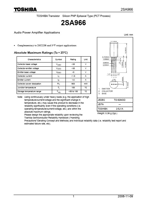
TOSHIBA Transistor Silicon PNP Epitaxial Type (PCT Process)2SA966Audio Power Amplifier Applications• Complementary to 2SC2236 and 3-W output applications.Absolute Maximum Ratings (Ta = 25°C)Characteristics Symbol Rating UnitCollector-base voltage V CBO −30 V Collector-emitter voltage V CEO −30 V Emitter-base voltage V EBO −5 V Collector current I C−1.5 AEmitter currentI E 1.5 A Collector power dissipation P C 900 mW Junction temperature T j 150 °C Storage temperature rangeT stg−55 to 150°CNote: Using continuously under heavy loads (e.g. the application of high temperature/current/voltage and the significant change in temperature, etc.) may cause this product to decrease in thereliability significantly even if the operating conditions (i.e. operating temperature/current/voltage, etc.) are within the absolute maximum ratings.Please design the appropriate reliability upon reviewing the Toshiba Semiconductor Reliability Handbook (“HandlingPrecautions”/Derating Concept and Methods) and individual reliability data (i.e. reliability test report and estimated failure rate, etc).Unit: mmJEDEC TO-92MOD JEITA ―TOSHIBA 2-5J1A Weight: 0.36 g (typ.)Electrical Characteristics (Ta = 25°C)Characteristics Symbol TestCondition MinTyp.Max UnitCollector cut-off current I CBO V CB = −30 V, I E = 0 ――−100nAEmitter cut-off current I EBO V EB = −5 V, I C = 0 ――−100nA Collector-emitter breakdown voltage V (BR) CEO I C = −10 mA, I B = 0 −30 ―― V Emitter-base breakdown voltage V (BR) EBO I E = −1 mA, I C = 0 −5 ―― VDC current gain h FE(Note)V CE = −2 V, I C = −500 mA 100 ― 320Collector-emitter saturation voltage V CE (sat)I C = −1.5 A, I B = −0.03 A ――−2.0V Base-emitter voltage V BE V CE = −2 V, I C = −500 mA ――−1.0V Transition frequency f T V CE = −2 V, I C = −500 mA ― 120 ― MHz Collector output capacitance C ob V CB = −10 V, I E = 0, f = 1 MHz ― 40 ― pF Note: h FE classification O: 100 to 200, Y: 160 to 320Markinglead (Pb)-free package orlead (Pb)-free finish.indicatorCollector current I C (mA)h FE – ICD C c u r re n t g a i n h F ECollector current I C (mA)V CE (sat) – I CC o l l e c t o r -e m i t t e r s a t u r a t i on v o l t a g eV C E (s a t ) (V )Base-emitter voltage V BE (V)I C – V BEC oll e c t o rc u r r e n t I C (m A )Ambient temperature Ta (°C)P C – TaC o l l e c t o r p owe r d i s s ip a t io n P C (W )Collector-emitter voltage V CE (V)Safe Operating AreaC o l l e c t o r c u r r e n t I C (A )1.00 0 20 40 60 80 100 120 140 160 1800.20.40.60.8−−−−−−−−−−−−−−−−−−Collector-emitter voltage V CE (V)I C – V CEC o l l e c t o r c u r r e n t I C (m A )−−−−−−−−−−−−−−−−−RESTRICTIONS ON PRODUCT USE20070701-EN •The information contained herein is subject to change without notice.•TOSHIBA is continually working to improve the quality and reliability of its products. Nevertheless, semiconductor devices in general can malfunction or fail due to their inherent electrical sensitivity and vulnerability to physical stress. It is the responsibility of the buyer, when utilizing TOSHIBA products, to comply with the standards of safety in making a safe design for the entire system, and to avoid situations in which a malfunction or failure of such TOSHIBA products could cause loss of human life, bodily injury or damage to property.In developing your designs, please ensure that TOSHIBA products are used within specified operating ranges as set forth in the most recent TOSHIBA products specifications. Also, please keep in mind the precautions and conditions set forth in the “Handling Guide for Semiconductor Devices,” or “TOSHIBA Semiconductor Reliability Handbook” etc.• The TOSHIBA products listed in this document are intended for usage in general electronics applications (computer, personal equipment, office equipment, measuring equipment, industrial robotics, domestic appliances, etc.).These TOSHIBA products are neither intended nor warranted for usage in equipment that requires extraordinarily high quality and/or reliability or a malfunction or failure of which may cause loss of human life or bodily injury (“Unintended Usage”). Unintended Usage include atomic energy control instruments, airplane or spaceship instruments, transportation instruments, traffic signal instruments, combustion control instruments, medical instruments, all types of safety devices, etc.. Unintended Usage of TOSHIBA products listed in his document shall be made at the customer’s own risk.•The products described in this document shall not be used or embedded to any downstream products of which manufacture, use and/or sale are prohibited under any applicable laws and regulations.• The information contained herein is presented only as a guide for the applications of our products. No responsibility is assumed by TOSHIBA for any infringements of patents or other rights of the third parties which may result from its use. No license is granted by implication or otherwise under any patents or other rights of TOSHIBA or the third parties.• Please contact your sales representative for product-by-product details in this document regarding RoHS compatibility. Please use these products in this document in compliance with all applicable laws and regulations that regulate the inclusion or use of controlled substances. Toshiba assumes no liability for damage or losses occurring as a result of noncompliance with applicable laws and regulations.。
![5.2.1 国外品牌手机话机锁解锁指令及方法速查[共5页]](https://img.taocdn.com/s1/m/75ef786e1a37f111f0855b5f.png)
第5章手机解锁指令及方法速查131续表品牌型号其他解密功能及方法康佳C928、C936……需要使用解锁软件才能解开话机锁。
另外,C958、C968、A06、A98、D108、R608、R718、KC66、KC88、KC627、KC826等型号手机的解锁方法也相同K5238 输入指令“*5238*00#”可解个人信息密码琐3288 输入解锁指令“*6608866#”可解个人信息密码锁5238 输入解锁指令“*5238*00#”可解个人信息密码锁科健3000 输入指令“*#9918*106*1647#”或“*#9918*106*6538#”即可解决不能使用充值卡充值的问题美辰系列型号可使用串号解锁法,打开串号解锁软件,输入手机串号(格式是“******—**—******—*”,其中横杠是空格),输入正确后按“回车”键即可计算出锁机码,即界面第4行的后8位数,然后开机输入“#9917*”+8位解锁码+“#”即可恢复出厂设置并解锁首信C5066、C5068、C5288……输入指令“*#9922#”(无卡),可看settsing(设置)输入指令“*#9999#”可使手机复位,输入指令“*#06#”可查看串号另外,C6268、C6568等型号手机的指令也相同厦华2000 长按“C”键可以消除屏幕右下角的笑脸5.2 国外品牌手机解锁指令5.2.1 国外品牌手机话机锁解锁指令及方法速查品牌型号话机锁解锁指令及方法阿尔卡特BE4、BE5输入指令“83227423”即可解开话机锁另外,OT301、302、303等型号手机的解锁指令和方法也相同HD1、HE1输入指令“25228352”即可解开话机锁,输入指令“###847#”也可解锁。
另外,OT500、700等型号手机的解锁指令和方法也相同OT501 输入指令“###847#”即可解开话机锁,另外,OT511等型号手机的解锁指令和方法也相同OT735 输入指令“83227423”即可解开话机锁,另外,535等型号手机的解锁指令和方法也相同爱立信T36、T28 输入指令“*#0000#”即可将爱立信老型号手机的菜单恢复到英语菜单,同时解开话机锁388、398 在手机显示“phone locked”或“话机已锁”时,只要输入指令“0000”,即可解开话机锁飞利浦系列型号在待机状态下,输入指令“*#7489*#”,即可显示和更改手机密码并解锁另外,DIGA、GENIE系列手机的解锁指令和方法也相同FIZZ 输入指令“*#1234*#”可以查看密码并解开话机锁S568 输入指令“*01763*737381#”即可解开话机锁168C 输入指令“*#2254*#”即可解开话机锁630 输入指令“#20021208”按“发射”键即可解开话机锁828 输入指令“*#7489*#”即可通过显示和更改手机密码进行解锁泛泰PG8000 输入指令“*01763*737381#”即可解开话机锁7870 不装卡输入指令“*4955#”后,手机进入工程模式,选择消除所有密码,即可解开CPU锁好彩K896输入指令“*2580*#”(第一个“*”要按两次,否则按不出来),进入手机测试模式,选择恢复出厂设置,即可解开话机锁338输入指令“**2580*#”进入手机工程模式,选择第6项码片复位,即可解开话机锁(同时会清除手机中的电话号码,最好用试机卡)韩国蓝星 V268……插卡开机后输入指令“0124”即可解开话机锁另外,V268+等型号手机的解锁指令和方法也相同LG GSM全系列不插卡开机输入指令“2945#*#”,选第6项Factory Reset(恢复出厂值),即可解开话机锁,这个方法还可以解决一些手机的开机定屏问题(通常出现在不插卡正常,插卡定屏的那些型号上)ALL……输入指令“2945#*#”即可解开话机锁另外,LG 2G等型号手机的解锁指令和方法也相同。

Copyright © 2017 Moxa Inc. Released on December 28, 2017About MoxaMoxa is a leading manufacturer of industrial networking, computing, and automationsolutions. With over 25 years of industry experience, Moxa has connected more than 30 million devices worldwide and has a distribution and service network that reachescustomers in more than 70 countries. Moxa delivers lasting business value by empowering industry with reliable networks and sincere service for automation systems. Information about Moxa’s solutions is available at . You may also contact Moxa by email at *************. How to Contact Moxa Tel: +886-2-8919-1230 How to Use the TIA Portal to Set a Siemens PLC and the MGate 5111Moxa Technical Support Team****************Contents1 Application Description ...................................................................2 2 System Topology .............................................................................3 3Required Equipment and Components (4)A. TIA Portal .................................................................................................... 4B. Modbus Slave .............................................................................................. 4C.MGate 5111 Firmware (4)D. MGate 5111’s GSD File (4)4MGate 5111 Setting (5)A. Protocol Conversion ...................................................................................... 5B. Configure Modbus Commands ........................................................................ 5C.Configure PROFIBUS Module (7)D. I/O Data Mapping (8)5 Siemens PLC Setting ....................................................................... 9 6Communication Test (21)A. Status Monitoring ........................................................................................21 B. Fault Protection . (27)1Application DescriptionThe TIA Portal is Siemens’s new software platform to configure and programS7-300/400/1200/1500 PLCs. This technical note demonstrates how to configure theSiemens S7-300 to connect with the MGate 5111 in TIA Portal V14.The MGate 5111 supports a variety of maintenance functions, such as Protocol Diagnostics, Traffic Monitoring, Status Monitoring, and Fault Protection. The Status Monitoringfunction notifies a PLC/DCS/SCADA system when a Modbus device gets disconnected or does not respond. If a command has run successfully, the status bit’s value will be 1. If a command has failed, the status bit’s value will be 0. In this case, the master device will be aware of the failure status of the slave device. When a PROFIBUS cable gets disconnected, the Fault Protection function executes actions on end devices identified by a pre-defined value set by the user.This technical note demonstrates how PROFIBUS Master (Siemens PLC) get these Modbus command statuses by receiving Input Status module values, as well as how the FaultProtection function works. We also demonstrate how Protocol Diagnostics and TrafficMonitoring make troubleshooting easy.2System TopologyThis technical note demonstrates how to exchange data between a PROFIBUS master and six Modbus TCP slaves. The Modbus TCP slave IDs 1-3 use Modbus Read command and show the Status Monitoring function. The Modbus TCP slave IDs 4-6 use Modbus Write command and show the Fault Protection function.We use the Siemens S7-300 as the PROFIBUS Master to connect the MGate 5111’s PROFIBUS port. On a PC, we run a Modbus Slave tool to simulate Modbus TCP slaves that the MGate 5111 will connect to the PC’s TCP 502 to poll slaves.3Required Equipment and ComponentsA.TIA PortalAs a registered Siemens’s customer you can download the trial software for TIA PortalV14 and test it for 21 days.Version: V14Download Website:https:///cs/document/109740158/simatic-step-7-(tia-portal)-v14-trial-download?dti=0&lc=en-WWB.Modbus SlaveModbus Slave is a popular Modbus slave simulator to test and debug your modbusdevices. Supports Modbus RTU/ASCII and Modbus TCP/IP.Version: V6+Download Website:/download.htmlC.MGate 5111 FirmwareVersion: V.1.0Download Website: D.MGate 5111’s GSD FileThe GSD (General Station Description) file is an electronic device datasheet or device database file that identifies the PROFIBUS IO device. This file can be installed into a PROFIBUSEngineering tool, e.g., TIA Portal so that the PROFIBUS Engineering tool can configure thisPROFIBUS IO Device.Version: V.1.0 or higherDownload Website: Note: For wiring, please refer to the MGate 5111 User’s Manual4 MGate 5111 SettingFor details, please refer to the MGate 5111 user’s manual that you can download from A. Protocol ConversionLogin to the MGate 5111’s Web Console. Set Protocol Conversion : Role 1 as PROFIBUS Slave and Role 2 as TCP Client.B. Configure Modbus CommandsUnder Modbus TCP settings , set Max. retry as 0. The default value is 3. Changing this value to 0 is in order to quickly demonstrate the detection that the TCP command has failed.Then add below Function Code 03 commands to poll Slave ID1- ID3’s register 0, and add Function Code 06 commands to write Slave ID4-ID6’s register 0.Keep ID4’s Fault Protection command as Keep latest data.For ID5 Fault Protection command, choose Clear all data bit to 0 and set Fault timeout as 10000 ms.For ID6 Fault Protection command, choose Set to user defined value and set Fault value as 0xFF 0xFF. Fault timeout is set as 10000 ms.C.Configure PROFIBUS ModuleAdd Input Module 1 words to Slot 1-3 to map the register values of Modbus Slave ID 1-3.Add Input Status Module to store the Modbus TCP command status on Slot 4. AddOutput: 1 word modules to slots 5-7 to write the value on the registers of Modbus Slave IDs 4~6.D. I/O Data MappingLet the MGate auto map the data on both sides of the MGate’s IO Internal Memory. Modbus read commands fit PROFIBUS Module 1-3 as below. Take note that the input status module is not included in MGate’s IO Internal Memory.On the other data flow, we can see PROFIBUS Modules 5-7 fit ID4 and ID5’s Modbus write commands as follows:5Siemens PLC Setting(1)Create a new project.(2)Once the new project has been created successfully, click Configure a device toadd the PLC.To add the actual PLC’s CPU model, select it from Controllers CPU as below:(3) Click PLC’s PROFINET interface to set its IP Address .(4)Click PLC’s MPI/DP interface to set Interface Type as PROFIBUS.Click Add new subne t to add a PROFIBUS subnet.Then a PROFIBUS_1 subnet is created. You can modify the PROFIBUS baudrate by modifying Transmission Speed5111’s GSD file.Select the MGate 5111’s GSD file then click Install .Make sure the installation is a success.(6)In the Hardware catalog window, we can filter “moxa” to search the MGate 5111. Choose the MGate 5111 device icon, then drag and drop to PROFIBUS_1 subnet.(7) Click Not assigned to assign the MGate 5111 to PLC_1.Then the MGate 5111 is set into PLC_1’s DP Master System.(8) In the MGate 5111’s Device view , drag and drop Input 1 Word to Slot 1-3 and Input 1 Byte to Slot 4. Assign their I address to 0-6.Drag and drop Output 1 Word to Slot 5-7. Assign their Q address to 0-5.(9) Under the MGate 5111’s Properties , set its PROFIBUS address as its actual address, which is set by hardware’s rotary switch.(10)We want to get Modbus ID1-ID3’s register value and make sure the Modbuscommands’ responses are valid. If a Modbus command’s response is invalid or times out, the register value will show a specific value. In this demonstration, we will use a program to set this value as 0xFFFF. We will show details later.We created the following tags:Each Network program shows as follows:(11)Execute Compile and make sure there are no errors.(12)Execute DownloadClick Start Search to search for an accessible PLC.After locating an accessible PLC, execute Load .The TIA Portal will check hardware and software consistency. After checking for errors, click Load to download.After loading, enable Start all to start modules and then click Finish.6Communication TestA.Status Monitoring(1)The PC runs a Modbus Slave tool and listens on TCP port 502. Add slave IDs 1-3and set their register 0’s value as 1, 2, 3, respectively.(2)Click Add new watch table to create the Watch table_1.Add the following tags to be monitored:(3)Click Go online and then click Monitor all.When Input Status module shows a value of 7, then commands 1-3 are successful.ID1Value- ID3Value are running as 1, 2, 3, respectively.(4) We can use the MGate’s Protocol Diagnostics tool on the Web Console to checkModbus and PROFIBUS communication status:Via System Monitoring → Protocol Status → Modbus TCP Diagnose , we can see its connection status is OK with no invalid responses.Via System Monitoring → Protocol Status → Modbus TCP Traffic , we can log Modbus TCP communication traffic:Via System Monitoring → Protocol Status → PROFIBUS Slave Diagnose , we can see State’s value is note as Data Exchange :Via System Monitoring → Protocol Status → I/O Data View , we can choose PROFIBUS Master ← Modbus TCP Server data flow side to see Modbus slave input data:(5)Disable Modbus Slave ID 2 on the Modbus Slave tool, so Modbus Command 2can’t receive any responses. Check Watch table; Input Status module showsa value of 5 and ID2Value a value of 0xFFFF.Disable Modbus Slave ID 1 and 3 on the Modbus Slave tool. Check Modbus TCP Diagnose;Status shows that the Request_timeout and Timeout counters are increasing:B. Fault Protection(1)Add slave ID4-ID6 on the Modbus Slave tool as below:(2) On the Watch table, set Modify value on QW0 as 0x0004, QW2 as 0x0005, QW4 as 0x0006. Then click the Modify button.(3) Check Modbus Slave IDs 4-6; they are updated as 0x0004, 0x0005, 0x0006, respectively.Via System Monitoring → Protocol Status → I/O Data View, we can choosePROFIUS Master → Modbus/TCP Server data flow side to see the PROFIBUS output data:(4)Remove the PROFIBUS cable. After 10000 ms, the Fault Timeout is on. Checkwhether Modbus Slave ID 4’s register 0 value is still 0x0004. Slave ID 5’s register0 value is updated to 0x0000 and Slave ID 6’s register 0 to 0xFFFF.Check PROFIBUS Master Modbus/TCP Server data flow side. We can see they all updated as its Fault Value:Check PROFIBUS Slave. Its Baudrate shows Not Found and State shows Wait Parameterization:。

M A X262中文资料(总5页) -CAL-FENGHAI.-(YICAI)-Company One1-CAL-本页仅作为文档封面,使用请直接删除在电子电路中,滤波器是不可或缺的部分,其中有源滤波器更为常用。
一般有源滤波器由运算放大器和RC元件组成,对元器件的参数精度要求比较高,设计和调试也比较麻烦。
美国Maxim公司生产的可编程滤波器芯片MAX262可以通过编程对各种低频信号实现低通、高通、带通、带阻以及全通滤波处理,且滤波的特性参数如中心频率、品质因数等,可通过编程进行设置,电路的外围器件也少。
本文介绍MAX262的情况以及由它构成的程控滤波器电路。
1 MAX262芯片介绍MAX262芯片是Maxim公司推出的双二阶通用开关电容有源滤波器,可通过微处理器精确控制滤波器的传递函数(包括设置中心频率、品质因数和工作方式)。
它采用CMOS工艺制造,在不需外部元件的情况下就可以构成各种带通、低通、高通、陷波和全通滤波器。
图1是它的引脚排列情况。
图1 MAX262引脚V+ ——正电源输入端。
V- ——负电源输入端。
GND ——模拟地。
CLKA ——外接晶体振荡器和滤波器A 部分的时钟输入端,在滤波器内部,时钟频率被2分频。
CLKB ——滤波器B 部分的时钟输入端,同样在滤波器内部,时钟频率被2分频。
CLKOUT ——晶体振荡器和R-C振荡的时钟输出端。
OSCOUT ——与晶体振荡器或R-C振荡器相连,用于自同步。
INA、INB ——滤波器的信号输入端。
BPA、BPB——带通滤波器输出端。
LPA、LPB——低通滤波器输出端。
HPA、HPB——高通、带阻、全通滤波器输出端。
WR ——写入有效输入端。
接V+时,输人数据不起作用;接V-时,数据可通过逻辑接口进入一个可编程的内存之中,以完成滤波器的工作模式、f0及Q的设置。
此外,还可以接收TTL电平信号,并上升沿锁存输人数据。
A0、A1、A2、A3 ——地址输人端,可用来完成对滤波器工作模式、f0和Q的相应设置。

gmsl max9296a原理
GMSL (Gigabit Multimedia Serial Link)是一种高速、高带宽的
串行接口技术,广泛应用于多媒体传输领域。
而Max9296A
是一种GMSL收发器芯片,它的原理主要涉及以下几个方面:
1. 串行传输:Max9296A采用串行传输方式,通过一对差分线
对数据进行传输。
这种传输方式可以提供更高的带宽和更远的传输距离。
2. 差分信号传输:Max9296A采用差分信号传输方式,通过同
时传输正负两个信号来抵消传输过程中的噪声和干扰。
这种传输方式可以提高信号质量和抗干扰能力。
3. 视频数据传输:Max9296A主要用于传输视频数据,支持高
清视频格式(如1080p、4K等)。
它可以将视频数据转换为
串行信号,并通过差分线进行传输。
4. 时钟和同步信号:Max9296A通过发送时钟和同步信号来保
持数据传输的同步性。
时钟信号用于确定数据传输的速率和时序,同步信号用于确定数据传输的起始和结束点。
5. 电源管理:Max9296A具有电源管理功能,可以根据需要对
芯片进行供电和休眠控制,以降低功耗和延长芯片的使用寿命。
总之,Max9296A通过使用GMSL技术的串行传输和差分信号传输方式,以及时钟和同步信号的控制,实现了高速、高带宽
的视频数据传输。
同时,它还具有电源管理功能,方便对芯片进行供电和控制。


General DescriptionThe MAX2605–MAX2609 evaluation kits (EV kits) simplify evaluation of this family of voltage-controlled oscillators (VCOs). These kits enable testing of the devices’ per-formance and require no additional support circuitry.Both signal outputs use SMA connectors to facilitate connection to RF test equipment.These EV kits are fully assembled and tested. Their oscil-lation frequencies are set to approximately the midrange of the respective VCOs.Featureso Easy Evaluationo Complete, Tunable VCO Test Board with Tank Circuit o Low Phase Noiseo Fully Assembled and TestedEvaluate: MAX2605–MAX2609MAX2605–MAX2609 Evaluation Kits19-1673 Rev 0; 9/00Ordering InformationComponent SuppliersFor free samples and the latest literature, visit or phone 1-800-998-8800.For small orders, phone 1-800-835-8769.MAX2606 Component ListMAX2605 Component ListE v a l u a t e : M A X 2605–M A X 2609MAX2605–MAX2609 Evaluation Kits 2_______________________________________________________________________________________Quick StartThe MAX2605–MAX2609 evaluation kits are fully assembled and factory tested. Follow the instructions in the Connections a nd Setup section for proper device evaluation.Test Equipment Required•Low-noise power supplies (these are recommended for oscillator noise measurement). Noise or ripple will frequency-modulate the oscillator and cause spectral spreading. Batteries can be used in place of power supplies, if necessary.– Use a DC power supply capable of supplying +2.7V to +5.5V. Alternatively, use two or three 1.5V batteries.– Use a DC power supply capable of supplying +0.4V to +2.4V, continuously variable, for TUNE.Alternatively, use two 1.5V batteries with a resistive voltage divider or potentiometer.•An RF spectrum analyzer that covers the operating frequency range of the MAX2605–MAX2609• A 50Ωcoaxial cable with SMA connectors •An ammeter (optional)Connections and Setup1)Connect a DC supply (preset to +3V) to the V CC and GND terminals (through an ammeter, if desired) on the EV kit.2)Turn on the DC supply. If used, the ammeter readingMAX2607 Component ListMAX2608 Component ListEvaluate: MAX2605–MAX2609MAX2605–MAX2609 Evaluation Kits_______________________________________________________________________________________3approximates the typical operating current specified in the MAX2605–MAX2609 data sheet.3)Connect the VCO output (OUT+ or OUT-) to a spec-trum analyzer with a 50Ωcoaxial cable.4)Apply a positive variable DC voltage between 0.4V and 2.4V to TUNE.5)Check the tuning bandwidth on the spectrum analyz-er by varying the tuning voltage (+0.4V to +2.4V).Layout ConsiderationsThe EV kit PC board can serve as a guide for laying out a board using the MAX2605–MAX2609. Generally, the VCC pin on the PC board should have a decoupling capacitor placed close to the IC. This minimizes noisecoupling from the supply. Also, place the VCO as far away as possible from the noisy section of a larger sys-tem, such as a switching regulator or digital circuits.The VCO ’s performance is strongly dependent on the availability of the external tuning inductor. For best per-formance, use high-Q components and choose their val-ues carefully. To minimize the effects of parasitic ele-ments, which degrade circuit performance, place the tuning inductor and C BYP close to the VCO. For higher-frequency versions, include the parasitic PC board inductance and capacitance when calculating the oscillation frequency. In addition, remove the ground plane around and under the tuning inductor to minimize the effect of parasitic capacitance.Noise on TUNE translates into FM noise on the outputs;therefore, keep the trace between TUNE and the control circuitry as short as possible. If necessary, use an RC filter to further suppress noise, as done on the EV kits.E v a l u a t e : M A X 2605–M A X 2609MAX2605–MAX2609 Evaluation Kits 4_______________________________________________________________________________________Figure 2. MAX2608/MAX2609 EV Kits SchematicFigure 1. MAX2605/MAX2606/MAX2607 EV Kits SchematicEvaluate: MAX2605–MAX2609MAX2605–MAX2609 Evaluation Kits_______________________________________________________________________________________5Figure 3. MAX2605/MAX2606/MAX2607 EV Kits ComponentPlacement Guide—Top Silk ScreenFigure 4. MAX2608/MAX2609 EV Kits Component PlacementGuide—Top Silk ScreenFigure 5. MAX2605/MAX2606/MAX2607 EV Kits PC BoardLayout—Component SideFigure 6. MAX2608/MAX2609 EV Kits PC Board Layout—Component SideMa xim ca nnot a ssume responsibility for use of a ny circuitry other tha n circuitry entirely embodied in a Ma xim product. No circuit pa tent licenses a re implied. Maxim reserves the right to change the circuitry and specifications without notice at any time.6_____________________Maxim Integrated Products, 120 San Gabriel Drive, Sunnyvale, CA 94086 408-737-7600©2000 Maxim Integrated ProductsPrinted USAis a registered trademark of Maxim Integrated Products.E v a l u a t e : M A X 2605–M A X 2609MAX2605–MAX2609 Evaluation Kits Figure 7. MAX2605/MAX2606/MAX2607/MAX2608/MAX2609EV Kits PC Board Layout—Ground Plane。

Max263(264)是开关电容有源滤波器设计用于精密滤波应用。
中心频率,Q,工作模式都可以通过输入引脚选择。
Max263不需要用外部元件去实现带通,低通,高通,全通滤波。
max263是专门带通应用程序和包含一个通用运算放大器。
两个第二阶滤波器部分都包含在这两个设备。
通过fclk/f0Max263和267的中心频率可以到达57KHZ,而max264和268可以到达140KHZ。
Max263(264)有28个引脚,max267(268)有24个引脚。
1、滤波器设计软件化2、中心频率32阶可控3、Q值128阶可控4、Q值与f0独立可编程5、f0可达140KHz6、支持+5V和士5V两种供电方式芯片诸引脚功能如下(括号内数字为引脚号):V+(10):供电正极, 并接旁路电容尽量靠近该脚V-(18):供电负极, 并接旁路电容尽量靠近该脚GND(19):模拟地CLKA(13):A单元元时钟输人, 该时钟在芯片内部被二分频CLKB(14):B单元时钟输人, 该时钟在芯片内部被二分频OSC OUT(20):连至晶体, 组成晶振电路(若接时钟信号时, 该脚不连)INA,INB(5,1):滤波器输人BPA,BPB(3,27): 带通输出LPA,LPB(2,28):低通输出HPA,HPB(4,26):高通、带陷、全通输出M0,M1(8,7):模式选择,+5V高,-5V低F0-F4(24,17,23,12,11):时钟与中心频率比值(FCLK/f0)编程端Q0-Q6(15,16,21,22,25,6,9):Q编程端。
1、供给电压士15V2、输入电压士0.3V3、输入电流士50Ma对M0、M1两个管脚编程可使芯片工作于模式1、2、3、4几种方式,对应的功能如表1所示。
时钟与中心频率比值与编码对应如表2所示。
模式1:当我们要实现全极点低通或带通滤波器如切比雪夫、巴特沃斯滤波器时这种模式是很有用的, 有时该模式也用来实现带陷滤波器, 但由于相关零极点位置固定, 使得用作带陷时受到限制。

The OnCell 5004/5104 are high-performance industrial grade cellular routers that allow up to 4 Ethernet-based devices to simultaneously use a single cellular data account for primary or backup network connectivity to remote sites and devices. Both products provide the functionality of a cellular router, firewall, and switch in one device. To ensure zero data lose and on-demand cellular communication, OnCell 5004/5104 are integrated with GuaranLink function. The difference between the OnCell 5004 and OnCell 5104 is that the OnCell 5104 comes with a built-in relay output that can be configured to indicate the priority of events when notifying or warning engineers in the field, and the two digital inputs allow you to connect basic I/O devices, such as sensors, to the cellular network. The OnCell 5004 can be placed on a desktop or wall-mounted, whereas the OnCell 5104 has an IA design and can be attached to a DIN-rail. Both products use 12 to 48 VDC power inputs with a screw-on design for greater reliability, and the Ethernet ports come with 1.5 KV magnetic isolation protection to keep your system safe from unexpected electrical discharges.OnCell 5004/5104 OnCell 5004OnCell 5104 SpecificationsOverviewCellular InterfaceStandards: GSM/GPRSBand Options: Quad-band 850/900 and 1800/1900 MHzGPRS Multi-slot Class: Class 10GPRS Terminal Device Class: Class BGPRS Coding Schemes: CS1 to CS4Tx Power: 1 watt GSM 1800/1900, 2 watts EGSM 850/900WAN InterfaceNumber of Ports: 1Ethernet: 10/100 Mbps, RJ45 connector, Auto MDI/MDIX Magnetic Isolation Protection: 1.5 KV built-inLAN InterfaceNumber of Ports: 4Ethernet: 10/100 Mbps, RJ45 connector, auto MDI/MDIX Magnetic Isolation Protection: 1.5 KV built-inSIM InterfaceNumber of SIMs: 2SIM Control: 3 VI/O Interface (OnCell 5104 only)Alarm Contact: 1 relay output with current carrying capacity of 1 A @ 24 VDCDigital Inputs: 2 electrically isolated inputs• +13 to +30 V for state “1” (On)• +3 to -30 V for state “0” (Off)SoftwareNetwork Protocols: UDP/TCP, SNTP, ICMP, DDNS, DHCP/BOOTP, PPPoE, PPP, DNS Relay, HTTPS, Telnet, IPSec Router/Firewall: NAT, port forwarding, routing Authentication: Local user-name and passwordSecurity: IP filteringManagement SoftwareOnCell Central Manager: Centralized management solution for accessing private IPs from the InternetPhysical CharacteristicsHousing: Aluminum, providing IP30 protectionWeight:OnCell 5004: 505±5 gOnCell 5104: 645±5 gDimensions:OnCell 5004: 158 x 103 x 35 mm (6.22 x 4.06 x 1.38 in) OnCell 5104: 135 x 50.8 x 103 mm (5.315 x 2.00 x 4.16 in) Environmental LimitsOperating Temperature: -30 to 55°C (-22 to 131°F) Storage Temperature: -40 to 75°C (-40 to 167°F)Ambient Relative Humidity: 5 to 95% (30°C, non-condensing) Power RequirementsNumber of Power Inputs: 1 terminal block, 1 power jack Input Voltage: 12 to 48 VDCPower Consumption:OnCell 5004: 12 to 48 VDC, 400mA (Idle), 900 mA (max.) OnCell 5104: 12 to 48 VDC, 450mA (Idle), 950 mA (max.)Standards and CertificationsSafety: UL 60950-1EMC: EN 55022 Class A, EN 55024, FCC Part 15 Subpart B Class A Radio: FCC Part 22H, FCC Part 24E, EN 301 489-1, EN 301 489-7, EN 301 511ReliabilityMTBF (mean time between failures): OnCell 5004: 352,000 hrs OnCell 5104: 480,000 hrsWarrantyWarranty Period: 5 yearsDetails: See /warrantyOrdering InformationAvailable ModelsOnCell 5004: 4-port 10/100M Ethernet to GSM/GPRS cellular routerOnCell 5104: 4-port 10/100M Ethernet to GSM/GPRS cellular router, IA designNote: Please visit Moxa’s website for a complete list of optional wireless accessories and antennas available for Moxa’s wireless products.。


General DescriptionThe MAX3362 low-power, high-speed transceiver for RS-485/RS-422 communication operates from a single +3.3V power supply. The device contains one differen-tial transceiver consisting of a line driver and receiver.The transceiver operates at data rates up to 20Mbps,with an output skew of less than 6ns. Driver and receiv-er propagation delays are guaranteed below 50ns. This fast switching and low skew make the MAX3362 ideal for multidrop clock/data distribution applications.The output level is guaranteed at +1.5V with a standard 54Ωload, compliant with RS-485 specifications. The transceiver draws 1.7mA supply current when unloaded or fully loaded with the drivers disabled.Additionally, the MAX3362 has a low-power shutdown mode, reducing the supply current to 1µA.The MAX3362 has a 1/8-unit-load receiver input imped-ance, allowing up to 256 transceivers on the bus. The MAX3362 is designed for half-duplex communication.The device has a hot-swap feature that eliminates false transitions on the data cable during circuit initialization.The drivers are short-circuit current limited, and a ther-mal shutdown circuit protects against excessive power dissipation.The MAX3362 is available in an 8-pin SOT package and specified over industrial and automotive tempera-ture ranges.ApplicationsClock/Data Distribution Telecom Equipment Security EquipmentPoint-of-Sale Equipment Industrial ControlsFeatureso Space-Saving 8-Pin SOT Package o Guaranteed 20Mbps Data Rate o Operates from a Single +3.3V Supply o 6ns (max) Transmitter and Receiver Skew o Hot-Swap Featureo Interoperable with +5V Logico Allows up to 256 Transceivers on the Bus o 1µA Low-Power Shutdown Mode o 1.7mA Operating Supply Current o -7V to +12V Common-Mode Range o Current Limiting and Thermal Shutdown o Half-Duplex Operationo Automotive Temperature Range VariantsMAX33623.3V , High-Speed, RS-485/RS-422 Transceiver inSOT Package________________________________________________________________Maxim Integrated Products 1Ordering Information19-2218; Rev 1; 5/02For pricing, delivery, and ordering information,please contact Maxim/Dallas Direct!at 1-888-629-4642, or visit Maxim’s website at .Typical Operating CircuitPin Configuration and Functional Diagram appear at end of data sheet.M A X 33623.3V , High-Speed, RS-485/RS-422 Transceiver in SOT Package 2_______________________________________________________________________________________ABSOLUTE MAXIMUM RATINGSDC ELECTRICAL CHARACTERISTICS(V= +3.3V ±5%, T = T to T , unless otherwise noted. Typical values are at V = +3.3V and T = +25°C.) (Notes 1, 2)Stresses beyond those listed under “Absolute Maximum Ratings” may cause permanent damage to the device. These are stress ratings only, and functional operation of the device at these or any other conditions beyond those indicated in the operational sections of the specifications is not implied. Exposure to absolute maximum rating conditions for extended periods may affect device reliability.All voltages with respect to GND.V CC , RE , DE, DI ......................................................-0.3V to +6V Receiver Input Voltages, Driver OutputVoltages (A, B).......................................................-8V to +13V Receiver Input Current, Driver OutputCurrent (A, B).................................................................250mA |V A - V B |..................................................................................+8V Receiver Output Voltage (RO)....................-0.3V to (V CC + 0.3V)Continuous Power Dissipation (T A = +70°C)8-Pin SOT (derate 9.7mW/°C above +70°C) ...............777mW Operating Temperature RangeMAX3362E__ ..................................................-40°C to +85°C MAX3362A__ ................................................-40°C to +125°C Storage Temperature Range.............................-65°C to +150°C Junction Temperature......................................................+150°C Lead Temperature (soldering, 10s).................................+300°CMAX33623.3V , High-Speed, RS-485/RS-422 Transceiver inSOT PackageDC ELECTRICAL CHARACTERISTICS (continued)(V= +3.3V ±5%, T = T to T , unless otherwise noted. Typical values are at V = +3.3V and T = +25°C.) (Notes 1, 2)SWITCHING CHARACTERISTICS (MAX3362E_ _ only)(V CC = +3.3V ±5%, T A = T MIN to T MAX , unless otherwise noted. Typical values are at V CC = +3.3V and T A = +25°C.) (Note 1)M A X 33623.3V , High-Speed, RS-485/RS-422 Transceiver in SOT Package 4_______________________________________________________________________________________Note 2:All currents into the device are positive; all currents out of the device are negative. All voltages are referenced to deviceground, unless otherwise noted.Note 3:∆V OD and ∆V OC are the changes in V OD and V OC , respectively, when the DI input changes state.Note 4:The short-circuit output current applies to peak current just prior to foldback-current limiting; the short-circuit foldback out-put current applies during current limiting to allow a recovery from bus contention.Note 5:Shutdown is enabled by bringing RE high and DE low. If the enable inputs are in this state for less than 50ns, the device isguaranteed not to enter shutdown. If the enable inputs are in this state for at least 600ns, the device is guaranteed to have entered shutdown.Note 6:Transition time from shutdown mode to normal operation.SWITCHING CHARACTERISTICS (MAX3362E_ _ only)(continued)(V = +3.3V ±5%, T = T to T , unless otherwise noted. Typical values are at V = +3.3V and T = +25°C.) (Note 1)MAX33623.3V , High-Speed, RS-485/RS-422 Transceiver inSOT Package_______________________________________________________________________________________5Typical Operating Characteristics(V CC = +3.3V, T A = +25°C, unless otherwise noted.)010520153530254001.00.51.52.02.53.03.5OUTPUT CURRENT vs. RECEIVER OUTPUTLOW VOLTAGEM A X 3362 t o c 01RECEIVER OUTPUT LOW VOLTAGE (V)O U T P U T C U R R E N T (m A )-30-20-25-10-15-5001.52.00.51.02.53.03.5OUTPUT CURRENT vs. RECEIVER OUTPUTHIGH VOLTAGEM A X 3362 t o c 02RECEIVER OUTPUT HIGH VOLTAGE (V)O U T P U T C U R R E N T (m A )3.223.233.253.243.26-40-1053550-25658095110125RECEIVER OUTPUT HIGH VOLTAGEvs. TEMPERATUREM A X 3362 t o c 03TEMPERATURE (°C)R E C E I V E R O U T P U T H I G H V O L T A G E (V )2000.010.020.030.040.05-40-105-25203550658095110125RECEIVER OUTPUT LOW VOLTAGEvs. TEMPERATUREM A X 3362 t o c 04TEMPERATURE (°C)R E C E I V E R O U T P U T L O W V O L T A G E (V )DRIVER OUTPUT CURRENTvs. DIFFERENTIAL OUTPUT VOLTAGEM A X 3362 t o c 05DIFFERENTIAL OUTPUT VOLTAGE (V)D R I VE R O U T P U T C U R R E N T (m A )3.23.02.82.62.4153045607502.23.4DRIVER DIFFERENTIAL OUTPUT VOLTAGEvs. TEMPERATURETEMPERATURE (°C)D R I VE R D IF F E R E N T I A L O U T P U T V O L T AG E (V )1109580655035205-10-250.51.01.52.02.53.00-40125DRIVER OUTPUT CURRENT vs. DRIVER OUTPUT LOW VOLTAGEM A X 3362 t o c 07DRIVER OUTPUT LOW VOLTAGE (V)D R I VE R O U T P U T C U R R E N T (m A )11108923456711020304050607080901001101201300012DRIVER OUTPUT CURRENT vs. DRIVER OUTPUT HIGH VOLTAGEM A X 3362 t o c 08DRIVER OUTPUT HIGH VOLTAGE (V)D R I VE R O U T P U T C U R R E N T (m A )4312-5-4-3-2-10-6-130-120-110-100-90-80-70-60-50-40-30-20-10010-140-75SUPPLY CURRENT vs. TEMPERATUREM A X 3362t o c 09TEMPERATURE (°C)I C C (m A )11095-25-10535506520801.691.701.711.721.731.741.751.761.68-40125M A X 33623.3V , High-Speed, RS-485/RS-422 Transceiver in SOT Package 6_______________________________________________________________________________________SHUTDOWN SUPPLY CURRENTvs. TEMPERATUREM A X 3362 t o c 10TEMPERATURE (°C)I S H D N (µA )1109580655035205-10-250.20.40.60.81.01.21.40-40125DRIVER OUTPUT SKEW vs. TEMPERATUREM A X 3362 t o c 11TEMPERATURE (°C)D R I VE R O U T P U T S K E W (n s )110956580-105203550-250.020.040.060.080.100.120.140.160.180.200.220.240.260-40125252729313335RECEIVER PROPAGATION DELAYvs. TEMPERATUREM A X 3362 t o c 12R E C E I V E R P R O P AG A T I O N D E L A Y (n s )-40-1053550-25658095110125TEMPERATURE (°C)2020ns/divUNLOADED DRIVER OUTPUTWAVEFORMM A X 3362 t o c 13B3.3Vf DIN = 16MbpsA20ns/divLOADED DRIVER OUTPUTWAVEFORMM A X 3362 t o c 14B2Vf DIN = 16Mbps R L = 54ΩA20ns/divDRIVER PROPAGATION DELAYMAX3362 toc15Af DIN = 16MbpsDIN2V/divB3.3V20ns/divRECEIVER PROPAGATION DELAYMAX3362 toc16ROf DIN = 16MbpsA2V/div2V/divBTypical Operating Characteristics (continued)(V CC = +3.3V, T A = +25°C, unless otherwise noted.)MAX33623.3V , High-Speed, RS-485/RS-422 Transceiver inSOT Package_______________________________________________________________________________________7Figure 2. Driver Timing Test CircuitFigure 3. Driver Propagation DelayFigure 1. Driver DC Test Load Figure 4. Driver Enable and Disable Times (t PDSL , t PDZL , t PDLS ,t PDLZ )M A X 33623.3V , High-Speed, RS-485/RS-422 Transceiver in SOT Package 8_______________________________________________________________________________________Figure 5. Driver Enable and Disable Times (t PDSH , t PDZH , t PDHS , t PDHZ)Figure 6. Receiver Propagation DelaysMAX33623.3V , High-Speed, RS-485/RS-422 Transceiver inSOT Package_______________________________________________________________________________________9Detailed DescriptionThe MAX3362 low-power, high-speed transceiver for RS-485/RS-422 communication operates from a single +3.3V power supply. The device contains one differen-tial line driver and one differential line receiver. The dri-ver and receiver may be independently enabled. When disabled, outputs enter a high-impedance state.The transceiver guarantees data rates up to 20Mbps,with an output skew of less than 6ns. This low skew time makes the MAX3362 ideal for multidrop clock/datadistribution applications, such as cellular base stations.Driver and receiver propagation delays are below 50ns.The output level is guaranteed at 1.5V on a standard 54Ωload.The device has a hot-swap feature that eliminates false transitions on the data cable during circuit initialization.Also, drivers are short-circuit current limited and are protected against excessive power dissipation by ther-mal shutdown circuitry.Figure 7. Receiver Enable and Disable TimesM A X 33623.3V , High-Speed, RS-485/RS-422 Transceiver in SOT Package 10______________________________________________________________________________________The MAX3362 has a 1/8-unit-load receiver input imped-ance, allowing up to 256 transceivers to be connected simultaneously on a bus. The MAX3362 is designed for half-duplex communication.DriverThe driver transfers single-ended input (DI) to differen-tial outputs (A, B). The driver enable (DE) input controls the driver. When DE is high, driver outputs are enabled.These outputs are high impedance when DE is low. When the driver is enabled, setting DI low forces the noninverting output (A) low and inverting output (B)high. Conversely, drive DI high to force noninverting output high and inverting output low (Table 1).Drive RE high and DE low (disable both receiver and driver outputs) to enter low-power shutdown mode.ReceiverThe receiver reads differential inputs from the bus lines (A, B) and transfers this data as a single-ended output (RO). The receiver enable (RE ) input controls the receiver. Drive RE low to enable the receiver. Driving RE high places RO into a high-impedance state. When the receiver is enabled, RO is high if (A-B) ≥200mV. RO is low if (A-B) ≤-200mV.Drive RE high and DE low (disable both receiver and driver outputs) to enter low-power shutdown mode.Hot-Swap CapabilityHot-Swap InputWhen circuit boards are inserted into a hot or powered backplane, disturbances to the enable and differential receiver inputs can lead to data errors. Upon initial cir-cuit board insertion, the processor undergoes its power-up sequence. During this period, the output dri-vers are high impedance and are unable to drive the DE input of the MAX3362 to a defined logic level.Leakage currents up to 10µA from the high-impedance output could cause DE to drift to an incorrect logic state. Additionally, parasitic circuit board capacitance could cause coupling of V CC or GND to DE. These fac-tors could improperly enable the driver.When V CC rises, an internal pulldown circuit holds DE low for at least 10µs and until the current into DE exceeds 200µA. After the initial power-up sequence,the pulldown circuit becomes transparent, resetting the hot-swap tolerable input.Hot-Swap Input CircuitryThe MAX3362 enable inputs feature hot-swap capability.At the input there are two NMOS devices, M1 and M2(Figure 8). When V CC ramps from 0, an internal 10µs timer turns on M2 and sets the SR latch, which also turns on M1. Transistors M2, a 300µA current sink, and M1, a 30µA current sink, pull DE to GND through an 8k Ωresis-tor. M2 is designed to pull DE to the disabled state against an external parasitic capacitance up to 100pF that may drive DE high. After 10µs, the timer deactivates M2 while M1 remains on, holding DE low against three-state leakages that may drive DE high. M1 remains on until an external source overcomes the required input current. At this time, the SR latch resets and M1 turns off.When M1 turns off, DE reverts to a standard, high-impedance CMOS input. Whenever V CC drops below 1V, the hot-swap input is reset.For RE there is a complimentary circuit employing two PMOS devices pulling RE to V CC .Hot-Swap Line TransientThe circuit of Figure 9 shows a typical offset termination used to guarantee a greater than 200mV offset when a line is not driven (the 50pF represents the minimum parasitic capacitance that would exist in a typical appli-cation). During a hot-swap event when the driver isMAX33623.3V , High-Speed, RS-485/RS-422 Transceiver inSOT Package______________________________________________________________________________________11Figure 8. Simplified Structure of the Driver Enable Input (DE)Figure 9. Differential Power-Up Glitch (Hot Swap)10µs/divFigure 10. Differential Power-Up Glitch (0.1V/µs)M A X 33623.3V , High-Speed, RS-485/RS-422 Transceiver in SOT Package 12______________________________________________________________________________________connected to the line and is powered up the driver must not cause the differential signal to drop below 200mV. Figures 10, 11, and 12 show the results of the MAX3362 during power-up for three different V CC ramp rates (0.1V/µs, 1V/µs, and 10V/µs). The photos show the V CC ramp, the single-ended signal on each side of the 100Ωtermination, as well as the differential signal across the termination.Low-Power Shutdown ModeLow-power shutdown mode is initiated by bringing both RE high and DE low. I n shutdown, the MAX3362 typi-cally draws only 1µA supply current.RE and DE may be driven simultaneously; the device is guaranteed not to enter shutdown if RE is high and DE is low for less than 50ns. If the inputs are in this state for at least 600ns, the device will enter shutdown.Enable times t PDZH, t PDZL, t PRZH and t PRZL in the Switching Characteristics table assume the device was not in a low-power shutdown state. Enable times t PDSH,t PDSL, t PRSH,and t PRSL assume the device was shut down. Drivers and receivers take longer to become enabled from low-power shutdown mode than from driver/receiver disable mode.Applications InformationPropagation DelaysFigures 5 and 6 show the typical propagation delays.Skew time is simply the difference between the low-to-high and high-to-low propagation delay. Small driver/receiver skew times help maintain a symmetrical mark-space ratio (50% duty cycle). Both the receiver skew time and driver skew time are under 6ns.256 Transceivers on the BusThe standard RS-485 receiver input impedance is 12k Ω(one-unit load), and a standard driver can drive up to 32 unit loads. The MAX3362 transceiver has a 1/8-unit-load receiver input impedance (96k Ω), allowing up to 256 transceivers to be connected in parallel on one communication line. Any combination of these devices and/or other RS-485 transceivers with a total of 32 unit loads or less can be connected to the line.Driver Output ProtectionTwo mechanisms prevent excessive output current and power dissipation caused by faults or by bus con-tention. The first, a foldback current limit on the output stage, provides immediate protection against short cir-cuits over the whole common-mode voltage range (see Typical Operating Characteristics ). The second, a ther-mal shutdown circuit, forces the driver outputs into a high-impedance state if the die temperature becomes excessive.Typical ApplicationsThe MAX3362 transceiver is designed for bidirectional data communications on multipoint bus transmission lines. The Typical Operating Circuit shows a typical net-work applications circuit. To minimize reflections, the line should be terminated at both ends in its character-istic impedance, and stub lengths off the main line should be kept as short as possible.1µs/divFigure 11. Differential Power-Up Glitch (1V/µs)200ns/divFigure 12. Differential Power-Up Glitch (10V/µs)MAX33623.3V , High-Speed, RS-485/RS-422 Transceiver inSOT Package______________________________________________________________________________________13Pin ConfigurationFunctional DiagramChip InformationTRANSISTOR COUNT: 708PROCESS: BiCMOSM A X 33623.3V , High-Speed, RS-485/RS-422 Transceiver in SOT Package Maxim cannot assume responsibility for use of any circuitry other than circuitry entirely embodied in a Maxim product. No circuit patent licenses are implied. Maxim reserves the right to change the circuitry and specifications without notice at any time.14____________________Maxim Integrated Products, 120 San Gabriel Drive, Sunnyvale, CA 94086 408-737-7600©2002 Maxim Integrated ProductsPrinted USAis a registered trademark of Maxim Integrated Products.Package Information(The package drawing(s) in this data sheet may not reflect the most current specifications. For the latest package outline information,go to /packages .)。
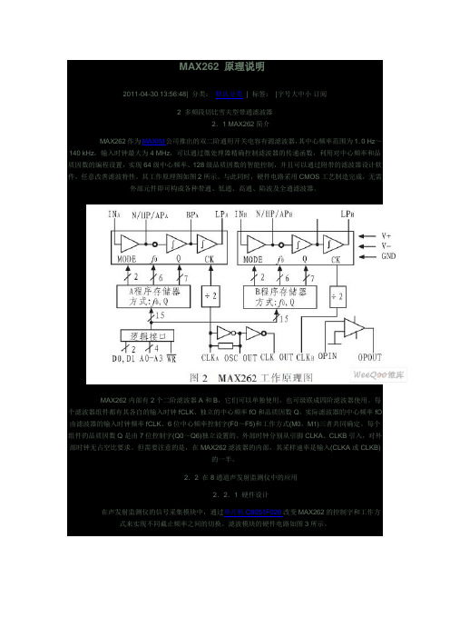
MAX262 原理说明2011-04-30 13:56:48| 分类:默认分类| 标签:|字号大中小订阅2 多频段切比雪夫型带通滤波器2.1 MAX262简介MAX262作为MAXIM公司推出的双二阶通用开关电容有源滤波器,其中心频率范围为1.0 Hz ~140 kHz,输入时钟最大为4 MHz,可以通过微处理器精确控制滤波器的传递函数,利用对中心频率和品质因数的编程设置,实现64级中心频率、128级品质因数的智能控制,并且可以通过附带的滤波器设计软件,任意改善滤波特性。
其工作原理图如图2所示。
与此同时,硬件电路采用CMOS工艺制造完成,无需外部元件即可构成各种带通、低通、高通、陷波及全通滤波器。
MAX262内部有2个二阶滤波器A和B,它们可以单独使用,也可级联成四阶滤波器使用。
每个滤波器组件都有其各自的输入时钟fCLK、独立的中心频率fO和品质因数Q。
实际滤波器的中心频率fO 由滤波器的输入时钟频率fCLK、6位中心频率控制字(F0~F5)和工作方式(M0,M1)三者共同确定。
每个组件的品质因数Q是由7位控制字(Q0~Q6)独立设置的。
外部时钟分别从引脚CLKA、CLKB引入,对外部时钟无占空比要求。
但需要注意的是,在MAX262滤波器的内部,其采样速率是输入(CLKA或CLKB)的一半。
2.2 在8通道声发射监测仪中的应用2.2.1 硬件设计在声发射监测仪的信号采集模块中,通过单片机C8051F020改变MAX262的控制字和工作方式来实现不同截止频率之间的切换。
滤波模块的硬件电路如图3所示。
MAX262内部的两个二阶滤波器是完全独立的,利用MAX262内部的滤波器A实现低通滤波,滤波器B实现高通滤波,再将两个滤波器级联起来,以实现满足系统设计要求的四阶切比雪夫型带通滤波器。
由于低通三档和高通三档所要求的截止频率都是低频且间隔宽,所以针对不同的截止频率和工作模式,在不超过MAX262的比率的范围情况下,必须提供多种不同的时钟频率。

DATA SHEET Flex Max ®RF Amplifiers FM9021.2 GHz Bridger AmplifierFor cable operators looking to ensure maximum backward compatibility, scalability, and protect network investments, CommScope offers solutions that deliver new services with minimal CAPEX, enhance network efficiency, and increase subscriber satisfaction.The new CommScope 1.2 GHz Flex Max ®FM902 Bridger Amplifier enables cable operators to take advantage of DOCSIS 3.1 efficiencies while maintaining backward compatibility with existing 750 MHz, 870 MHz, and 1 GHz systems.•Supports 1.2 GHz Downstream and 204 MHzUpstream bandpass for DOCSIS ®3.1 migration•Modular RF Electronics package with upgradablefrequency split options•Increased gain to allow drop in upgrades for≥ 750 MHz spacing•Mechanically compatible with legacy Flex Net700/800/900 series and Flex Max 900 and 901series housings•Expanded return path bandwidth with support upto 204 MHz•QAM and analog ADU options for automatic levelcontrol and gain hold in the event of pilot loss FEATURESDownstreamThe new FM902 Bridger amplifier is equipped with Gallium Nitride (GaN) technology and two high level driven RF outputs. Each output port can be split with optional plug‐in Distribution accessories to enable a total of four ports.New 1.2 GHz Forward Cable Equalizers (CE‐120‐*) and Cable Simulators (CS‐120‐*) are available to optimize system designs. These new plug‐ins are in the JXP‐style form factor and plug into a carrier board with a backward compatible footprint so that operators who want to use the new amplifiers in older 870 MHz or 1 GHz systems can re‐use their SEQ‐* equalizers. The FM902 utilizes pluggable diplex filters, which provides operators with the flexibility to change band splits in the future.The following frequency splits are available:•5 to 42 MHz/54 to 1218 MHz (042 split)•5 to 85 MHz/102 to 1218 MHz (085 split)•5 to 204 MHz/258 to 1218 MHz (204 split)The FM902 is available pre‐configured with multiple Automatic Level Control (ALC) options that include 499.25 MHz for analog pilots or 609 MHz and 711 MHz for QAM pilot frequencies. These new pluggable Drive units are not backward compatible with previous FlexMax amplifiers. All amplifiers feature an Automatic/Manual mode jumper that can be set to enable the amplifier to operate in a Manual Level Control (MLC) or Thermal Gain Control (TGC) mode. The amplifier utilizes a gain hold feature in the event of pilot loss for added system reliability. There is an LED indicator to provide visual confirmation of the selected mode and pilot presence.UpstreamThe FM902 features 27 dB of gain in the upstream to accommodate a variety of network designs including high split. The upstream circuitry includes an attenuator location prior to the input test points that allows operators to achieve the recommended input levels. The return equalizer maintains the legacy MEQ‐**‐* form factor from the Flex Max series amplifiers and operators can select from a range of values based on their network design. Previous generation MEQT return path equalizers are no longer required because of the FM902’s on‐board thermal compensation feature, which helps maintain levels over temperature. There is also a new plug‐in Low Pass filter to provide additional high frequency signal isolation from the downstream signal path.Backward CompatibilityThe FM902 is available as a complete amplifier station or as a drop‐in RF module for economical upgrades of legacy C‐COR 750 MHz and 870 MHz FlexNet bridger amplifiers or FM901 1 GHz amplifiers. The FM902 features internal ‐20 dB test points only; there is no option for external test points. The RF module, however, can be installed into an earlier housing that does support external test points without invoking mechanical interference.COMPATIBILITY700900900901 Upgrade to Flex Max FM902Yes Yes Yes Yes Yes204 Split258–1218 Flatness, dB2±1.0 Operational Gain, dB347 minInternal Slope, dB4042 Split085 Split204 Split 21.0 19.4 15.5Noise Figure, dB8Test Points, dB‐20 ±1.0 Return Loss, dB516Hum Modulation @ 15A, dBc6 F minfwd to 870 MHz871 to 1003 MHz1004 to 1218 MHz ‐60‐55‐50Distortion: 1.2 GHz Analog/Digital, 30 Analog/124 Digital Channels7Reference Frequency, MHz1218/258/54Reference Input Level, dBmV10/8.2/10 (virtual)Reference Output Level (21 dB Slope), dBmV57/39.7/36 (virtual)Composite Triple Beat (CTB), dBc‐70Composite Second Order (CSO), dBc‐76Carrier to Composite Noise (CCN), dB856Distortion: 1.2 GHz All Digital, 190 Digital ChannelsReference Frequency, MHz1218/258/54Reference Input Level, dBmV4/2.2/4 (actual)Reference Output Level (21 dB Slope), dBmV51/33.7/30 (actual)Carrier to Composite Noise (CCN), dB849Modulation Error Rate (MER), dB948 minNOTES:1.Downstream bandwidth is determined by the diplex filters, forward flatness correction board, and high pass filter installed in the amplifier.2.Flatness is measured with respect to slope. Slope is calculated using least squares.3.Includes forward equalizer loss and gain reserve for proper AGC operation.4.Specified from 54 to 1218 MHz,5.0 dB Linear Slope plus 16.0 dB Cable Slope.5.Measured with jumpers in the Distribution accessory location.6.Hum modulation is measured at 15 Amps AC current passing through the port under test (13 Amps AC for ports 2 and 5).7.30 analog channels from 55.25 MHz to 253.25 MHz, 124 digital QAM channels from 261 MHz to 999 MHz, and a 192 MHz wide OFDM channel centered at 1122 MHz. The digitalchannels are at a level 6 dB below the analog. The output level is 57 dBmV (virtual) at 1218 MHz, with 21 dB tilt from 54 MHz to1218 MHz.N is measured by turning off the QAM/OFDM channel under test and inserting a CW test signal at the corresponding QAM/OFDM RF level in its place.9.The MER is calculated from the measured CCN.SPECIFICATIONSAC Input Current (Typical) 1.0 A/36 W @ 45 V0.8 A/36 W @ 60 V0.7 A/37 W @ 90 VAC Input Voltage Range, VAC 40–90AC Bypass Current, A1513 (Port 2 and Port 5)Operating Temperature Range‐40°to +60°C ‐40°to +140°F Housing Dimensions, L x W x D16.0 L x 10.7 W x 5.35 D inches 406 L x 272 W x 136 D mm Weight 16 lbs7.3 kg204 Split 5–204Flatness, dB 2±0.5Operational Gain, dB 327Reference Operating Slope, dB 0 ±0.75Noise Figure, dB 48Test Points, dB ‐20 ±1.0Return Loss, dB 5,616Hum Modulation @ 15A, dBc 75 to 10 MHz11 to F maxreturn MHz ‐50‐60Distortion: All Digital, 6 Digital Channels 8Reference Frequency, MHz42/5Reference Input Level, dBmV13/13Reference Output Level, dBmV40/40NPR Dynamic Range, dB 929BER Dynamic Range, dB 1035Distortion: All Digital, 13Digital Channels 8Reference Frequency, MHz85/5Reference Input Level, dBmV9/9Reference Output Level, dBmV36/36NPR Dynamic Range, dB 926BER Dynamic Range, dB 1032Distortion: All Digital, 33 Digital Channels 8Reference Frequency, MHz204/5Reference Input Level, dBmV6/6Reference Output Level, dBmV33/33NPR Dynamic Range, dB 922BER Dynamic Range, dB 1028NOTES:1.Upstream bandwidth is determined by the diplex filters, low pass filter (RPLPF), and upstream equalizer (MEQ) installed in the amplifier.2.Flatness is measured with respect to slope. Slope is calculated using Least Squares.3.Includes return equalizer loss and gain reserve for proper AGC operation.4.Noise figure is at T a = 25 ±5°C. The noise figure may degrade by up to 1 dB over the operating temperature range and will degrade by 3 dB typical when a Splitter is installed in the Distribution accessory location.5.The return loss from 5–15 MHz may degrade by up to 1 dB over the operating temperature range.6.Measured with jumpers in the Distribution accessory location.7.Hum modulation is measured with 15 Amps AC current passing through the port under test (13 Amps AC current for ports 2 and 5). Hum mode can degrade by up to 5 dB from 5–10 MHz at ‐40°C.8.The QAM load is 256 QAM, J.83 Annex B, 5.360537 MS/s; 6 MHz/channel.9.The NPR dynamic range is specified for an NPR greater than or equal to 40 dB.10.The BER dynamic range is specified for an uncorrected (Pre ‐FEC) BER less than or equal to 1.0 x 10‐6.Note: Specifications are subject to change without notice.Copyright Statement:©2022CommScope,Inc.All rights reserved.ARRIS,the ARRIS logo,and Flex Max are trademarks of CommScope,Inc.and/or its affiliates.All other trademarks are the property of their respective owners.No part of this content may be reproduced in any form or by any means or used to make any derivative work (such as translation,transformation,or adaptation)without written permission from CommScope,Inc and/or its affiliates (“CommScope”).CommScope reserves the right to revise or change this content from time to time without obligation on the part of CommScope to provide notification of such revision or change.Contact Technical Services for product support:•United States: +1‐888‐944‐4357•International: +1‐215‐323‐2345RELATED PRODUCTSADU/QADUSS ‐1218‐2 Splitters FM332 1.2 GHz Line ExtenderInstallation Services SDC ‐1218‐* DirectionalCouplers Forward Signal Correction Plug ‐in Accessories1.2 GHz FM902 BRIDGER AMPLIFIER ORDERING GUIDEIn the example below, part number FMB12X085‐SHG6C1N corresponds to the shaded rows in the Key Guide.F M B 12X 085—S HG 6C 1N REQUIRED ACCESSORIESModel NameDescription CE ‐120‐*CS ‐120‐*Forward 1.2GHzCableEqualizer 2 to 20 dB in 1 dB steps ‐or ‐Forward 1.2 GHz Cable Simulator 1 to 10 dB in 1 dB steps MEQ ‐**‐*Return Equalizer, 5–42 MHz (042 Split), 5–85 MHz (085 Split), 5–204 MHz (204 Split)NPB ‐*NPB ‐750Plug ‐in attenuator/pad (values 0 to 26 dB in 1 dB steps)Plug ‐in terminator (75 ohm)。

封闭式压缩机EMEM系列恩布拉科是全球制冷压缩机行业市场与技术领先的企业,被世界上要求最严格的冰箱及冷柜厂家所认可。
恩布拉科在中国恩布拉科于1995年在中国成立合资公司,在全球都属于最现代化的新厂也于前不久建成投产。
其研发中心代表了最先进的技术水平,为产品开发及应用提供服务,先进的生产设备为高质量提供了保障。
EM全球生产轨迹在中国新投产的EM压缩机是最新技术开发成果,畅销于世界各地。
也是恩布拉科连续二十年在产品与制造技术上不断投入的结晶。
3 能耗节省超过60%3 静音3 外观尺寸小一般技术参数1、启动、运转电压压缩机能在0.2Mpa(R600a、表压)或0.5Mpa(R134a、表压)平衡压力下在标称电压的85%下启动。
在不同的系统上可以在170V或240V下运转2、电机本目录下的压缩机配备单相、双极RSIR或RSCR(带运行电容)、低启动力柜电机,可应用于毛细管节流的系统,要求在平衡压力下启动3、附件发货条件3.1、压缩机内注油、干燥空气或者抽真空3.2、提供附件(如胶脚、启动PTC、PTC盖、过载保护器等),但不组装在压缩机上4、搬运压缩机不能倒置或倾斜储存压缩机必须平放安装5、注意事项压缩机经过抽真空状态后不能通过高压电或进行启动试验所有EM压缩机出厂前已经过1800V9/1秒测试压缩机内不得注入防冻剂;防冻剂对绝缘材料有各种影响胶堵只应在焊接三管前拔掉General Technical Information1. STARTING AND OPERATING CONDITION VOLTAGEThe EM compressors can start at 85% nominal voltage, with equalized pressures of up tp 0.2 Mpa (R 600a, gauge pressure), 0.5 Mpa (R 134a, gauge pressure). Depending on the working conditions and systems characteristics, the compressor can operate at voltages as low as 170V and as high as 240V.2. MOTORThe compressors in this chart are equipped with monophase, two poles, RSIR or RSCR (with run capacitor), low starting torque (LST) motors, suitable to use with capillary tubes systems, requiring equalized pressures to start.3. DELIVERY CONDITIONS OF ACCESSORY PARTS3.1 Compressors are delivered with oil and holding charge of dry air.3.2 Accessories, eg. Rubber grommets, starting PTC, PTC cover, overload protector and spacers are supplied not assembled tothe compressor.4. HANDLINGCompressor must not be turned upside down or inclined for storage.Compressor must be mounted in the upright position.5. WARNINGSCompressor must not be subjected to high voltage or starting test while under vacuum.All EM compressors have already been submitted to a 1800V high voltage teste for one second.Compressor must not be charged with antifreeze agents, as their use can have adverse effects on the insulating materials. Plugs should only be removed immediately before brazing connectors to system tubes.EM压缩机性能参数Technical Data of Compressors测试条件:蒸发-23.3°C(-10°F) 冷凝54.4°C(130°F) 吸气/环境32.2°C(90°F) 液体32.2°C(90°F)Test Conditions: Evaporating: -23.3°C (-10°F) | Condensing: 54.4°C (130°F) | Gas and Ambient: 32.2°C (90°F) | Liquid: 32.2°C (90°F)EM附件图纸Components DrawingsNomenclature - Compressor ModelMounting AccessoriesNumberComponentSpecification 1 Rubber grommet H: 17.0±0.52 Spacer (metal bushing)H: 17.0±0.53 Fixing bolt M6x304 Hexagon nutM65 Washer with ext. teeth Ø 6.46 Flat washerØ 6.47 Compressor base plate 8Mounting base45678123组装附件胶脚编号附件规格金属衬套螺栓螺母外齿垫圈平垫圈底脚板安装底版压缩机型命名Note: After replacement, the compressor and its accessories must have proper processing, and the components must be recycled according to the material group (ferrous, non-ferrous, polymers, oils, ...) directives. These recommendations are intended to minimize the adverse impacts that may be caused to the environment.注:压缩机被更换之后,压缩机及其附件必须妥善处理,零部件必须根据其材料(金属、非金属、塑料、油等)方面的指令重复利用。

D AKOTA U LTRASONICSUltrasonic Bolting Equipment,Transducers &AccessoriesModels: Comments Part #Mini-MaxIncludes new version 2.0 hardware platform,Z-156-0006and temperature connector for use withpart# A-156-8001.Max IIIncludes temperature connector for use withZ-197-0001pt# A-156-8001.Includes: MiniMax- Unit, 3 AA Batteries, 4 oz. Bottle of Couplant, USB Type A toType C Transfer Cable, Carrying Case, 10’ Lemo to Microdot Transducercable, PC Utility Software (download from website), Operation Manual andCertification.Max II – Unit, Lithium Pack, 4 oz. Bottle of Couplant, USB Type A to Type BTransfer Cable, Carrying Case, 10’ Lemo 00 to Microdot Transducer Cable,PC Utility Software (download from website), Operation Manual andCertification.Non-Magnetic Single Element Contact TransducersFastener Material Types: All metalsNote: Side or Top entry connector option availableDiameter Part # MHz Comments Connector Entry 1/8” T-5903-2875 5 Microdot Top1/8” T-4903-2875 5 Microdot Side1/8”T-5903-487510 Microdot Top1/8”T-4903-487510 Microdot Side1/4”T-5023-1855 2.25 Microdot Top1/4”T-4023-1855 2.25 Microdot Side1/4”T-5023-2855 5 Microdot Top1/4”T-4023-2855 5 Microdot Side1/4”T-5023-485510 Microdot Top1/4”T-4023-485510 Microdot Side1/2”T-5043-1855 2.25 Microdot Top1/2”T-4043-1855 2.25 Microdot Side 1/2”T-5043-2855 5 Microdot Top 1/2”T-4043-2855 5 Microdot SideDiameter Reference Comments WearfaceDiameterCrystalDiameter1/8” .230” 1/8”1/4” .355” 1/4”1/2” .605” 1/2” Note: Other configurations, connectors, and styles available upon request for an additional charge. These items are custom builds only.Magnetic Single Element Contact TransducersFastener Material Types: All metalsDiameter Part # MHz Comments Connector Entry 1/8” T-700-2405 5 Microdot Top1/8”T-700-440510 Microdot Top1/4”T-702-1405 2.25 Microdot Top1/4”T-702-2405 5 Microdot Top1/4”T-702-440510 Microdot Top3/8”T-703-1405 2.25 Microdot Top3/8”T-703-2405 5 Microdot Top1/2”T-704-1405 2.25 Microdot Top1/2”T-704-2405 5 Microdot Top3/4”T-706-1405 2.25 Microdot Top3/4”T-706-2405 5 Microdot TopDiameter Reference Comments OutsideDiameterWearfaceDiameterCrystalDiameter1/8” .380” .200” .125”1/4” .750” .320” .250”3/8” .810” .470” .375”1/2” 1.00” .630” .500”3/4” 1.21” .820” .750” Note: Other configurations, connectors, and styles available upon request for an additional charge. These items are custom builds only.Glue On Single Contact CrystalsFastener Material Types: All metalsGlue & Solvent: Loctite 425 & solvent 76820 X-NMS or equivalent.Note: For use on fasteners with limited elongation.Dimensions Part # MHz Comments Connector Entry1/10”x1/10” A-000-90037.5 Lot of 12 pcs N/A N/A1/8”x1/8” A-000-90017.5 Lot of 12 pcs N/A N/A1/8”x1/8” M-001-51407.5 Lot of 100 pcs w/coc N/A N/A Notes: M-001-5140: K81 crystal (Mat’l – Approx. 35% Lead, 60% Niobium, 5% Barium).Supplied with certificate of compliance with traceable lot ID and order #.*Additional frequencies & dimensions available as a custom build on request. Accessory ItemsInstrument & Carrying CasesPart # Description Comments F-149-0001MINI-MAX Instrument Case NylonA-149-6002MINI-MAX Instrument Case (v2.0) RubberE-200-0002MAX Instrument Case NylonF-250-0006MAX II Instrument Case NylonA-100-6003Plastic Carrying Brief Case MINI-MAXE-206-0001Plastic Carrying Case MAX onlyE-206-0002Plastic Carrying Case – Deluxe MAXA-250-6002Plastic Carrying Case MAX II only Transducer CablesLemo 00 M Lemo 00 F Microdot Part # Description Comments N-104-00204’ Single Lemo 00 to Microdot MAX & MINI-MAXN-106-00206’ Single Lemo 00 to Microdot MAX & MINI-MAXN-110-002010’ Single Lemo 00 to Microdot MAX & MINI-MAXN-110-602010’ Single Lemo 00 to Microdot (HighTemp, High Wear Teflon)MAX & MINI-MAXN-120-002020’ Single Lemo 00 to Micodot Single MAX & MINI-MAXN-120-602020’ Single Lemo 00 to Microdot (HighTemp, High Wear Teflon)MAX & MINI-MAXN-320-000020’ Lemo 00 2 pin to Lemo00 2 pin MINI-MAXN-104-00904’ Single Lemo 00 to Spring LoadedCenter Pin Fixture – Recessed Cap BoltsMAX & MINI-MAXN-704-00904’ Single Lemo 00 to Spring Loaded 2Pin fixture 1/4” SpacingMAX & MINI-MAXN-704-00944’ Single Lemo 00 to Spring Loaded 2Pin fixture 1/8” SpacingMAX & MINI-MAXA-000-90021/8” Magnetic Spring Loaded Center PinFixture – Hex Head BoltsMAX & MINI-MAXCustom All Configurations MAX & MINI-MAX CouplantPart # Description Comments V-000-0005 4 oz bottle (low viscosity) Standard V-000-0001 4 oz bottleV-000-000312 oz bottleV-000-0004 1 gallonCalibration BlocksPart # Description Mat’l Type X-000-0020Glass Calibration block (1", 2" , & 3") GlassX-000-00113” Steel Calibration Bar 4140 Steel X-000-00103” & 6” Steel Calibration Bars 4140 Steel Operation ManualsPart # Description Comments P-200-0002Operation Manual (MAX)P-156-0002Operation Manual (MINI-MAX)P-156-0005Operation Manual (MINI-MAX v2.0)P-197-0002Operating manual (MAX II)Misc. AccessoriesPart # Description CommentsA-167-5004High Speed Shut Off Box (control apump) – Direct HardwareMAX IIN-120-040020’ Lemo 1 (5 pin) to Lemo 00 cable MAX II Data Cables & AdaptersPart # Description Comments N-306-0010 6 foot RS232 ( DB-9 to lemo ) MINI-MAX N-406-0350 6 foot RS232 ( DB-9 M/F ) MAXN-402-0510USB to Serial Adapter MINI-MAX N-606-0530USB Type 1 to Type 2 female MAX II only N-110-047010’ Lemo 1 5pin to BNC analog out cable MAX II only N-110-041010’ Lemo 1 to 5pin DB9F serial out cable MAX II only N-003-0330USB-C to USB TYPE A 3’ data cable MINI-MAX v2.0N-306-0416Universal cable (5 pin Lemo 1 to BNC, 6’DB9, & 2 6’ Alarm out)MAX II onlyBattery Packs & ChargersPart # Description Comments B-040-3200Lithium ion battery pack MAX II only B-030-0000External smart battery charger MAX II only Line Power AdaptersPart # Description CommentsN-250-0001Power adaptor (12 volts @ 2 amps w/6”cable)MAX IIN-506-0060Universal Power Cord MAX & MAX II Temperature SensorsPart # Description CommentsA-156-8001Temperature Sensor w/6’ cable MINI-MAX &MAX IITransducer Diagrams1/8” Magnetic 1/4” Magnetic3/8” Magnetic1/2” Magnetic 3/4” Magnetic。

gmsl max9296a原理摘要:一、引言二、GMSL 和MAX9296A 的概述1.GMSL 的定义和作用2.MAX9296A 的功能和特点三、MAX9296A 的工作原理1.MAX9296A 的内部结构2.电源管理功能3.数据传输过程四、GMSL 和MAX9296A 在电子设备中的应用1.移动设备2.数据中心3.汽车电子五、结论正文:一、引言随着科技的飞速发展,电子设备的数据传输需求日益增长。
GMSL (General Mobile System Link)作为一种高速串行接口,满足了这一需求。
而MAX9296A 正是这样一款支持GMSL 协议的芯片,广泛应用于各种电子设备中。
本文将对GMSL 和MAX9296A 的原理进行详细解析。
二、GMSL 和MAX9296A 的概述1.GMSL 的定义和作用GMSL 是一种高速串行接口,主要应用于移动设备、汽车电子等领域,其数据传输速率最高可达6Gbps。
它通过简化电缆设计和降低系统成本,实现了设备间的高速数据传输。
2.MAX9296A 的功能和特点MAX9296A 是一款支持GMSL 协议的电源管理及数据传输芯片,具有高度集成、低功耗、高性能等特点。
它可以在单根电缆上实现电源和数据传输,简化了系统设计。
三、MAX9296A 的工作原理1.MAX9296A 的内部结构MAX9296A 内部集成了GMSL 收发器、电源管理电路、状态机等模块。
其中,GMSL 收发器负责数据传输;电源管理电路负责为整个系统提供稳定的电源;状态机则负责控制数据传输过程。
2.电源管理功能MAX9296A 的电源管理功能主要包括:为发送端和接收端提供3.3V 和1.8V 电源;根据GMSL 协议自动调整电源输出电压;实现电源的动态调整,以降低系统功耗。
3.数据传输过程在数据传输过程中,MAX9296A 通过GMSL 收发器实现数据的发送和接收。
数据发送时,发送端将数据通过差分对发送出去;数据接收时,接收端对接收到的数据进行差分信号处理,从而实现数据的正确传输。
General DescriptionThe MAX6391/MAX6392 microprocessor (µP) supervisory circuits provide sequenced logic reset outputs for multi-component or dual-voltage systems. Each device can monitor two supply voltages and time-sequence two reset outputs to control the order in which system components are turned on and off. The MAX6391/MAX6392 increase system reliability and reduce circuit complexity and cost compared to separate ICs or discrete components.The MAX6391/MAX6392 monitor V CC as the master reset supply. Both RESET1and RESET2are asserted whenever V CC drops below the selected factory-fixed reset threshold voltage. RESET1remains asserted as long as V CC is below the threshold and deasserts 140ms (min) after V CC exceeds the thresholds.RESET IN2 is monitored as the secondary reset supply and is adjustable with an external resistive-divider net-work. RESET2is asserted whenever either V CC or RESET I N2 is below the selected thresholds. RESET2remains asserted 140ms (min) or a capacitor-adjustable time period after V CC and RESET I N2exceed their thresholds. RESET2is always deasserted after RESET1during system power-up and is always asserted before RESET1during power-down.The MAX6391 includes two internal pullup resistors for RESET1and RESET2(the open-drain outputs can be externally connected to the desired pullup voltages).The MAX6392 includes an active-low manual reset input (MR ) that asserts both RESET1(push-pull) and RESET2(open drain).The MAX6391/MAX6392 are available in small 8-pin SOT23 packages and are specified over the -40°C to +85°C extended temperature range.ApplicationsComputers ControllersCritical µP Power Monitoring Set-Top Boxes PrintersServers/Workstations Industrial Equipment Multivoltage MonitoringFeatureso Preset V CC Reset Threshold Voltages from 1.58V to 4.63V (master supply)o Customer-Adjustable RESET IN2 to Monitor Voltages Down to 625mV (secondary supply) o Fixed (140ms min) R E S E T 1Timeout o Fixed (140ms min) or Customer-Adjustable R E S E T 2Timeout Period o Guaranteed Reset Valid to V CC = 1V o Active-Low Open-Drain Outputs or Push-Pull/Open-Drain Combinationo Internal Open-Drain Pullup Resistors (for external V OH voltage connections)o Manual Reset Input (MAX6392 only)o Immune to Short Negative V CC Transients o 15µA Typical Supply Current o Few External Components o Small 8-Pin SOT23 PackageMAX6391/MAX6392Dual-Voltage µP Supervisory Circuitswith Sequenced Reset Outputs________________________________________________________________Maxim Integrated Products1Pin ConfigurationsOrdering Information19-2210; Rev 1; 10/02*Insert the desired suffix (see Selector Guide) into the blanks to complete the part number. The MAX6391/MAX6392 require a 2.5k minimum order increment and are available in tape-and-reel only. Samples are typically available for standard versions (see Selector Guide for standard versions). Contact factory for availability.For pricing, delivery, and ordering information,please contact Maxim/Dallas Direct!at 1-888-629-4642, or visit Maxim’s website at .Typical Operating Circuit appears at end of data sheet.M A X 6391/M A X 6392Dual-Voltage µP Supervisory Circuits with Sequenced Reset Outputs 2_______________________________________________________________________________________ABSOLUTE MAXIMUM RATINGSELECTRICAL CHARACTERISTICSStresses beyond those listed under “Absolute Maximum Ratings” may cause permanent damage to the device. These are stress ratings only, and functional operation of the device at these or any other conditions beyond those indicated in the operational sections of the specifications is not implied. Exposure to absolute maximum rating conditions for extended periods may affect device reliability.V CC to GND...........................................................-0.3V to +6.0V RESET1(MAX6392), RESET IN2, CSRT,MR to GND..............................................-0.3V to (V CC + 0.3V)RESET1(MAX6391), RESET2, R1, R2 to GND......-0.3V to +6.0V Input Current (V CC , GND, CSRT, R1, R2, MR ).................±20mA Output Current (RESET1, RESET2)..................................±20mA Continuous Power Dissipation (T A = +70°C)8-Pin SOT23 (derate 5.26mW/°C above +70°C)...........421mWOperating Temperature Range ...........................-40°C to +85°C Junction Temperature......................................................+150°C Storage Temperature Range.............................-65°C to +150°C Lead Temperature (soldering, 10s).................................+300°CMAX6391/MAX6392Dual-Voltage µP Supervisory Circuitswith Sequenced Reset Outputs_______________________________________________________________________________________3ELECTRICAL CHARACTERISTICS (continued)(V CC = 1.2V to 5.5V, T A = T MIN to T MAX , unless otherwise specified. Typical values are at V CC = +5V and T A = +25°C.) (Note 1)Note 2:RESET2asserts before RESET1when V CC goes below the threshold for all supply voltage and temperature ranges.Note 3:CSRT must be connected to either V CC (for fixed RESET2timeout period) or an external capacitor (for user-adjustable RESET2timeout period).M A X 6391/M A X 6392Dual-Voltage µP Supervisory Circuits with Sequenced Reset Outputs 4_______________________________________________________________________________________Typical Operating Characteristics(V CC = +5V, T A = +25°C, unless otherwise noted.)10.811.011.411.211.611.8-4010-15356085RESET2 TO RESET1 DELAYvs. TEMPERATURETEMPERATURE (°C)D E L A Y (µs )200225250275300-40-1510356085RESET1 TIMEOUT PERIOD vs. TEMPERATUREM A X 6391 t o c 05TEMPERATURE (°C)T I M E O U T D E L A Y (m s )2.502.753.003.253.50-40-1510356085RESET1 TO RESET2 TIMEOUT PERIOD vs. TEMPERATURE (CSRT = 1500pF)M A X 6391 t o c 06TEMPERATURE (°C)T I M E O U T D E L A Y (m s )200225250275300-40-1510356085RESET1 TO RESET2 TIMEOUT PERIOD vs. TEMPERATURE (CSRT TIED TO V CC )M A X 6391 t o c 07TEMPERATURE (°C)T I M E O U T D E L A Y (m s )102040305060MAXIMUM TRANSIENT DURATION vs. RESET COMPARATOR OVERDRIVEOVERDRIVE (mV)M A X I M U M T R A N S I E N T D U R A T I O N (µs )11001010001716151413-4010-15356085SUPPLY CURRENT vs. TEMPERATUREM A X 6391 t o c 01TEMPERATURE (°C)S U P P L Y C U R R E N T (µA )202122232425262728-40-1510356085V CC FALLING TO RESET1 DELAY VS.TEMPERATUREM A X 6391 t o c 02TEMPERATURE (°C)D E L A Y (µs )91011121314151617-40-1510356085V CC FALLING TO RESET2 DELAYvs. TEMPERATUREM A X 6391 t o c 03TEMPERATURE (°C)D E L A Y (µs )MAX6391/MAX6392Dual-Voltage µP Supervisory Circuitswith Sequenced Reset Outputs_______________________________________________________________________________________5Detailed DescriptionEach device includes a pair of voltage monitors with sequenced reset outputs. The first block monitors V CC only (RESET1output is independent of the RESET IN2monitor). It asserts a reset signal (LOW) whenever V CC is below the preset voltage threshold. RESET1remains asserted for at least 140ms after V CC rises above the reset threshold. RESET1timing is internally set in each device. V CC voltage thresholds are available from 1.57V to 4.63V. I n all cases V CC acts as the master supply (all resets are asserted when V CC goes below its selected threshold). The V CC input also acts as the device power supply.The second block monitors both RESET IN2 and V CC . It asserts a reset signal (LOW) whenever RESET I N2 is below the 625mV threshold or V CC is below its reset threshold. RESET2remains asserted for a fixed 140ms(min) or a user-adjustable time period after RESET IN2rises above the 625mV reset threshold and RESET1is deasserted. Resets are guaranteed valid for V CC down to 1V.The timing diagram in Figure 2 shows the reset timing characteristics of the MAX6391/MAX6392. As shown in Figure 2, RESET1deasserts 140ms (min) (t RP1) after V CC exceeds the reset threshold. RESET2deasserts t RP2(140ms minimum or a user-adjustable timeout peri-od) after RESET I N2 exceeds 625mV and RESET1is deasserted. When RESET I N2 drops below 625mV while V CC is above the reset threshold, RESET2asserts within 10µs typ. RESET1is unaffected when this hap-pens. When V CC falls below V TH1, RESET2always asserts before RESET1(t RD2< t RD1).M A X 6391/M A X 6392Dual-Voltage µP Supervisory Circuits with Sequenced Reset Outputs 6_______________________________________________________________________________________Figure 1. Functional DiagramFigure 2. Timing DiagramMAX6391/MAX6392Dual-Voltage µP Supervisory Circuitswith Sequenced Reset Outputs_______________________________________________________________________________________7Applications InformationSelecting the Reset Timeout CapacitorThe RESET2delay may be adjusted by the user with an external capacitor connected from the CSRT pin to ground. The MAX6391 includes a 600nA current source that is switched to C CSRT to create a voltage ramp. The voltage ramp is compared to the internal 1.25V refer-ence to set the RESET2delay period. The period is cal-culated by:∆t = C ✕∆V/Iwhere ∆V = 1.25V, I = 600nA, and C is the external capacitor.Simplifying,t RP = 2.08 ✕106s / F ✕C CSRT For C CSRT = 1500pF, t RP = 3.1msA fixed internal 140ms (min) reset delay time for RESET2may be chosen by connecting the CSRT pin to V CC . The V CC to CSRT connection disables the voltage ramp and enables a separate fixed delay counterchain. The MAX6391 internally determines the CSRT connection and provides the proper timing setup.In all cases, RESET IN2 acts as the slave supply. V CC can assert the RESET2output but RESET IN2 will have no effect on the RESET1output.Monitoring Voltages Other Than V CCAn external resistive-divider network is required at RESET IN2 for most applications. The divider resistors,R3 and R4, may be calculated by the following formula:V RST = V TH2✕(R3 + R4)/R4where V TH2= 625mV (internal reference voltage) and V RST is the desired reset threshold voltage. R4 may be set to a conveniently high value (500k Ωfor example, to minimize current consumption) and the equation may be solved for R3 by:R3 = R4 ✕(V RST /V TH2- 1)For single-supply operations requiring two reset out-puts (RESET1before RESET2), connect RESET I N2directly to V CC and adjust RESET2timeout delay with C CRST as desired.Pullup ResistorsThe MAX6391 includes open-drain outputs for both RESET1and RESET2. Two internal resistors, R1 and R2, of 47k Ωeach are provided with internal connec-tions to RESET1and RESET2. These resistors may be connected to the appropriate external voltage for inde-pendent V OH drive with no additional component requirements.The MAX6392 includes a manual reset option, MR , that replaces the R1 pullup resistor. The active-low manual reset input forces both RESET1and RESET2low.RESET2is driven active before RESET1in all cases (10µs typ). The resets follow standard reset timing specifications after the manual reset is released. The manual reset is internally pulled up to V CC through a 47k Ωresistor.Negative-Going V CC TransientsIn addition to issuing a reset to the µP during power-up,power-down, and brownout conditions, these devices are relatively immune to short-duration, negative-going V CC or RESET I N2 transients (glitches). The Typical Operating Characteristics show the Maximum Transient Duration vs. Reset Comparator Overdrive graph. The graph shows the maximum pulse width that a negative-going V CC transient may typically have without issuing a reset signal. As the amplitude of the transient increas-es, the maximum allowable pulse width decreases.M A X 6391/M A X 6392Chip InformationTRANSISTOR COUNT: 810PROCESS: BiCMOSDual-Voltage µP Supervisory Circuits with Sequenced Reset Outputs 8_______________________________________________________________________________________Typical Operating CircuitMAX6391/MAX6392Dual-Voltage µP Supervisory Circuitswith Sequenced Reset OutputsMaxim cannot assume responsib ility for use of any circuitry other than circuitry entirely emb odied in a Maxim product. No circuit patent licenses are implied. Maxim reserves the right to change the circuitry and specifications without notice at any time.Maxim Integrated Products, 120 San Gabriel Drive, Sunnyvale, CA 94086 408-737-7600 _____________________9©2002 Maxim Integrated ProductsPrinted USAis a registered trademark of Maxim Integrated Products.Package Information(The package drawing(s) in this data sheet may not reflect the most current specifications. For the latest package outline information go to /packages .)。