模拟集成电路设计英文课件:Semi-conductor Device Physics
- 格式:ppt
- 大小:1.10 MB
- 文档页数:43


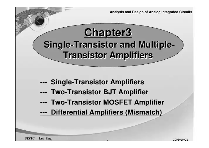
Chapter3Single-Transistor and Multiple-Transistor Amplifiers---Single-Transistor Amplifiers---Two-Transistor BJT Amplifier---Two-Transistor MOSFET Amplifier---Differential Amplifiers (Mismatch)DEVICE MISMATCH IN DIFEERENTIALAMPLIFIERSOutline---The general approach to analyzing mismatches ---Input voltage and current offset of BJTdifferential amplifiers---Input voltage offsets of MOS differential amplifiers---Small-Signal Characteristics of Unbalanced Diff.Amp.General MethodSuppose performance parameters p 1and p 2can be written as),,,(),,,(22221111L L z y x f p andz y x f p ==Ideally, x 1=x 2, y 1=y 2, z 1=z 2…,→p 1=p 2. But, in practice, they are not and an error exists:),,,,,,,(),(22211121L L z y x z y x f p p e Error ==where x1,y1,z1,…and x2,y2,z2,…can be expressed in terms of their difference and average values, For example,22121x x x andx x x +=−=∆MISMATCH ANALYSIS METHODS22121x x x andx x x +=−=∆xx x andxx x ∆−=∆+=⇒5.05.021thus,);5.0,5.0;5.0,5.0(),(21L y y y y x x x x f p p e ∆−∆+∆−∆+=Generally:x x <<∆, the following approximations canεεεε−≈++≈−111111orneglecting high power values of ).,.(2εεe i be concluded:INPUT VOLTAGE AND CURRENT OFFSET OF THE BJT DIFF. AMPLIFIERModel for Input Offset Voltage and CurrentBase width, base & collector doping level, effective emitter area, collector load resistance.•V OS :If v in =0)()(OS C TCOS C m C V R V I V R g v ∆=∆=∆If an offset exists in:21&C C R R )/(/)/()(_C C T m C C R OS C C C R R V g R v V R i v C ∆=∆=→∆=∆→If an offset exists in area or doping level, in I S)/(/)/(_/S S T m C I OS S C S V V S C I I V g i V I I I eI i S TBE ∆=∆=→∆=∆=∆→mOS C C C g V i i i =−=∆21•I OS :If an offset exists in i C ,→β/C OS i I ∆=)/)(/(/)()/)(/(/)/(__ββββββββC B OS C C C C C C R OS i i I i R R R R i I C ∆=∆=∆=∆=⇒RMS-sum (polarity of error is not important):2_2_2_2_&βOS R OS OS I OS R OS OS III VVV CSC+=+=DC performance:⎟⎟⎠⎞⎜⎜⎝⎛=⎟⎟⎠⎞⎜⎜⎝⎛−⎟⎟⎠⎞⎜⎜⎝⎛=⇒12212211ln ln ln S S C C T S C T S C T IDI I I I V I I V I I V V 22222221121121)()()()(A V Q D qn A V W N D qn I A V Q D qn A V W N D qn I CB B n i CB B A n i S CB B niCB B A n iS ====where W B (V CB )is the base width as a function of V CB , N A is theacceptor density in the base and A is the emitter area.122122110C C C C C C C C OD R R I I R I R I V =⇒=⇐=⎥⎦⎤⎢⎣⎡⎟⎟⎠⎞⎜⎜⎝⎛⎟⎟⎠⎞⎜⎜⎝⎛⎟⎟⎠⎞⎜⎜⎝⎛=⇒)()(ln 211212CB B CB B C C T OSV Q V Q A A R R V V 021=+−BE BE ID V V VNow, define:222&212121CC C C C C C C C C C C R R R and R R R R R R R R R ∆−=∆+=⇒+=−=∆222&212121AA A and A A A A A A A A A ∆−=∆+=⇒+=−=∆222&212121BB B B B B B B B B B B Q Q Q and Q Q Q Q Q Q Q Q Q ∆−=∆+=⇒+=−=∆Substituting these values into the expression for V OS gives⎥⎦⎤⎢⎣⎡⎟⎟⎠⎞⎜⎜⎝⎛∆−⎟⎠⎞⎜⎝⎛∆−⎟⎟⎠⎞⎜⎜⎝⎛∆−≈⎥⎥⎥⎥⎦⎤⎢⎢⎢⎢⎣⎡⎟⎟⎟⎟⎠⎞⎜⎜⎜⎜⎝⎛∆+∆−⎟⎟⎟⎟⎠⎞⎜⎜⎜⎜⎝⎛∆+∆−⎟⎟⎟⎟⎠⎞⎜⎜⎜⎜⎝⎛∆+∆−=B B C C T BB BB C C C C T OSQ Q A A R R V Q Q Q Q A A A A R R R R V V 111ln 222222ln BB C C Q Q and A A R R <<∆<<∆<<∆,Expanding the logarithm and neglecting higher order terms gives⎟⎟⎠⎞⎜⎜⎝⎛∆−∆−=⎟⎟⎠⎞⎜⎜⎝⎛∆+∆−∆−≈S S C C T B B C C T OSI I R R V Q Q A A R R V V whereBBS S Q Q A A I I ∆−∆=∆Example:05.0&01.0//==∆∆SSI IR R σσmV mV I I R R V V S S C C T OS 5.1)05.001.0)(26(−=+=⎟⎟⎠⎞⎜⎜⎝⎛∆−∆−≈mVmV V V SS CC I I R R T OS 3.1)05.0()01.0()26(22/2/2=+=+=∆∆σσCalculation of dV OS /dT:Assuming V OS (270C)=2mV,K V KmVT T V T V or I I R R T V T V OS OS S S C C T OS /67.63002)(µ=≈=∂∂⎟⎟⎠⎞⎜⎜⎝⎛∆+∆=∂∂Offset voltage can be cancelled using external circuitrybut to cancel the temperature drift, the external circuitry must have the temperature dependence.Temperature Dependence of the Input Offset VoltageThe input offset current of the BJT Differential Amplifier can be written as :112212215.0&5.0F C F C B B OS OS B B OS B B I I I I I I I I I I I ββ−=−=⇒−=+=Define:222&222&212112212112FF F F F F F F F F F F CC C C C C C C C C C C and I I I and I I I I I I I I I ββββββββββββ∆+=∆−=⇒+=−=∆∆+=∆−=⇒+=−=∆Input Offset Current of the BJT Differential AmplifierqCombining the previous expressions into the function for I OS gives:FF C C F F CC F C F FC C F F C C OS I I when I I I I I I I I βββββββββ<<∆<<∆⎟⎟⎠⎞⎜⎜⎝⎛∆−∆≈⎟⎟⎟⎟⎠⎞⎜⎜⎜⎜⎝⎛∆−∆−−∆+∆+=,2222, then,CCC C CC CCC C C C R R I I R R R R I I I I ∆=∆−⇒∆+∆−=∆+∆−21212121122122110C C C C C C C C OD R R I I R I R I V =⇒=⇐=Therefore,⎟⎟⎠⎞⎜⎜⎝⎛∆+∆−=FFC C F C OSR R I I βββINPUT VOLTAGE OFFSET OF THE MOSFETDIFF. AMPLIFIERModel for Input Offset Voltage•V OS : If v in =0mOS D D D g V i i i =−=∆21If an offset exists in:2/))(/(2/)/(_t GS D D D D D R OS V V R R I R v V D −∆=∆=→β21&D D R R LW k '=βDD D D D D R v i orR i v /)(∆=∆∆=∆→If),,('k L W or ∆∆∆∆β2/))(/(2/)/(2/)/(/_t GS D D D m D OS V V I I I g i V −∆=∆=∆=∆=βββββββββ),()(/)]}(2[2{/22_t tt tt GS t GS t t m D V OS V Vt small is V if V V V V V V V g i V t ∆<<∆∆∆≈−−∆+∆=∆=ββIf exists:•I OS =0tV ∆2'21'1212'221'1121)/(2)/(2)/(2)/(20L W k I L W k I V V L W k I V L W k I V V V V V D D t t D t D t ID GS GS ID −+−=−−+=⇒=+−122122110D D D D D D D D OD R R I I R I R I V =⇒=⇐=DC performance:Define:222&212121DD D D D D D D D D D D R R R and R R R R R R R R R ∆−=∆+=⇒+=−=∆222&212121ββββββββββββ∆−=∆+=⇒+=−=∆and 222&212121DD D D D D D D D D D D I I I and I I I I I I I I I ∆−=∆+=⇒+=−=∆222&212121tt t t t t t t t t t t V V V and V V V V V V V V V ∆−=∆+=⇒+=−=∆Substituting these values into the expression for V OS givestD D D t D D D D D t D D D D D tt t t D D D D OSV I I I V I I I I I V I I I I I V V V V I I I I V ∆+⎥⎦⎤⎢⎣⎡∆−∆=∆+⎥⎦⎤⎢⎣⎡∆+∆−−∆−∆+=∆+⎥⎦⎤⎢⎣⎡∆+∆−−∆−∆+=∆−−∆++⎟⎟⎠⎞⎜⎜⎝⎛∆−∆−−⎟⎟⎠⎞⎜⎜⎝⎛∆+∆+=βββββββββββββββββ222)221()221(2)21)(21()21)(21(2)2()2(5.05.025.05.02where,tt D D D D V V and I I R R <<∆<<∆<<∆<<∆,,,ββWhen the variation in 3 parameters are uncorrelated:mV V V R R V V V V t GS D D t GS t OS1072)(2)(22222=⎟⎟⎠⎞⎜⎜⎝⎛∆−+⎟⎟⎠⎞⎜⎜⎝⎛∆−+∆=ββVV V mV V R R t GS t D D 5.1&100%,5/%,1/=−=∆=∆=∆ββFor the correlated case:mV R R V V V V D D t GS t OS5522)(=⎟⎟⎠⎞⎜⎜⎝⎛∆+∆−−∆=ββ⎟⎟⎠⎞⎜⎜⎝⎛∆+∆−∆≈⇒∆−=∆βββ222D D D t OS D D D D R R I V V R R I I tGS DV V I −=β2⎟⎟⎠⎞⎜⎜⎝⎛∆+∆−−∆=⇒ββ22)(D D t GS t OSR R V V V VTemperature Dependence of the MOS InputOffset Voltage⎟⎟⎠⎞⎜⎜⎝⎛∆+∆−∆=βββ222D D D t OS R R I V V TT T T T T dT d T T T L WT k T )(5.1)/)((5.1)()()(5.1005.100'βββββ−=−=⇒⎟⎟⎠⎞⎜⎜⎝⎛==−−⎟⎟⎠⎞⎜⎜⎝⎛+∂∂⎟⎟⎠⎞⎜⎜⎝⎛∆+∆−=⎟⎟⎠⎞⎜⎜⎝⎛∂∂−∂∂⎟⎟⎠⎞⎜⎜⎝⎛∆+∆−=2/12/342322122 22122122βββββββββT I T I I R R T I T I I R R dT dV DD D D D D D D D D OSepredictabl T V T ∝epredictabl so not T T I D ∂∂∂∂β&R D , ,V tR C , (A, Q B ) →I SV OSV OS , I OS MOSFETBJT ↓⇒↑OS dm V A SUMMARYβ22221121221121R i R i v v v R i R i v v v c d +=+=−=−=2/)(,&,2/)(,21212121R R R R R R i i i i i i c d +=−=∆+=−=21R R ≠if:Definite:4)(2)2)(2()2)(2()()2)(2()2)(2(R i R i R R i i RR i i v R i R i RR i i RR i i v d cd c dc c cd d c dc d ∆+=∆−−+∆++=∆+=∆−−−∆++=Half circuitSMALL-SIGNAL CHARACTERISTICS ofUNBALANCED DIFF. AMP.2/)(,&,2/)(,21212121m m m m m m c d g g g g g g v v v v v v +=−=∆+=−=42)2)(2()2)(2( 22 )2)(2()2)(2( 221121221121d m c m d c mm d c m m m m c cm d m dc m md c m m m m d v g v g v v g g v v g g v g v g i i i v g v g v v g g v v g g v g v g i i i ∆+=−∆−++∆+=+=+=∆+=−∆−−+∆+=−=−=⇒21m m g g ≠Definite:if:22&0222=+∆+=∆++Rc idm m mid m Rd i v g v g v g v g i tail Rc ic tail ic r i v v v v 2+=−=)212()212(22tailm m tail m m ic tail m mtailm m id Rd r g g r g g v r g g r g g v i +∆+∆−++∆∆+−=tailm idm ic m Rc r g v g v g i 2122+∆+−=⇒⎟⎟⎠⎞⎜⎜⎝⎛+∆+∆−==+∆−∆∆+−====tail m m m v icoddmcm tailm m m tailm m v idod dmr g R g R g v v A r g Rg R g r g R g v v A id ic 21212220_0R i R i v RdRc od 222+∆=icdm cm id dm od v A v A v _+=Ri R i v Rc Rd oc +∆=22iccm id cm dm oc v A v A v +=_⎟⎟⎟⎟⎠⎞⎜⎜⎜⎜⎝⎛+∆∆+−==⎥⎥⎥⎥⎥⎥⎦⎤⎢⎢⎢⎢⎢⎢⎣⎡+⎟⎟⎠⎞⎜⎜⎝⎛⎟⎟⎠⎞⎜⎜⎝⎛∆∆−∆+∆−====tail m m m v ic oc cm tail m m m tail m m m m v id oc cm dm r g R g R g v v A r g g g r g R g R g R g v v A id ic2122212241020_SUMMARY•Differential Mode and Common Mode •Characteristics of Differential Amplifier •CMRR•ICMR•Offset Voltage•Mismatch。

模拟cmos集成电路设计英文版IntroductionA complementary metal-oxide-semiconductor (CMOS) integrated circuit (IC) is a type of electronic circuit that uses CMOS technology to integrate digital or analog circuits on a single chip. In this article, we will discuss the design process for a CMOS IC.Design flowThe design flow for a CMOS IC involves several stages, which are as follows:1. Requirements gathering: This stage involves gathering information about the requirements of the IC, such as its functionality, performance, and power requirements.2. Design specification: Based on the requirements gathered in the previous stage, a design specification is created that outlines the functional blocks of the IC, their interfaces, and their performance specifications.3. Circuit design: This stage involves designing the individual circuits that make up the IC, such as logic gates, amplifiers, and oscillators.4. Layout design: Once the circuits have been designed, the layout design stage involves placing the circuits on the chip and wiring them together.5. Simulation and verification: Simulation is used to verify the performanceof the circuits and the entire IC before it is fabricated.6. Tape-out: This is the process of preparing the design files for fabrication.Fabrication processThe fabrication process of a CMOS IC involves several steps, which are as follows:1. Substrate preparation: The starting material for the IC is a silicon wafer, which is coated with a layer of oxide.2. Gate oxidation: A thin layer of oxide is grown on the wafer surface where the gates of the transistors will be located.3. Poly-Si deposition: A layer of polycrystalline silicon (poly-Si) is deposited on the gate oxide layer.4. Photolithography: A series of masks are used to define the pattern of the transistors, interconnects, and other features on the chip.5. Etching: Chemical etching is used to remove the unwanted material from the wafer surface.6. Implantation: Ions are implanted into the wafer to create the source, drain, and gate regions of the transistors.7. Metal deposition: A layer of metal is deposited on top of the transistorsand interconnects for electrical contacts.8. Planarization: Chemical-mechanical polishing is used to planarize the surface of the chip.9. Packaging: The IC is packaged in a protective casing and tested for functionality and performance.ConclusionThe design and fabrication of a CMOS IC involves a complex process that requires expertise in multiple areas, such as digital and analog circuit design, layout design, and fabrication technology. However, the resulting IC can be a powerful tool for a wide range of applications, from consumer electronics to industrial control systems.。