
HVR-2X0620A中文资料
- 格式:pdf
- 大小:49.27 KB
- 文档页数:1


P/N: 1802021503014 *1802021503014*NPort W2150A/W2250A SeriesQuick Installation GuideEdition 6.1, September 2017Technical Support Contact Information/supportMoxa Americas:Toll-free: 1-888-669-2872 Tel: 1-714-528-6777 Fax: 1-714-528-6778 Moxa China (Shanghai office): Toll-free: 800-820-5036 Tel: +86-21-5258-9955 Fax: +86-21-5258-5505 Moxa Europe:Tel: +49-89-3 70 03 99-0 Fax: +49-89-3 70 03 99-99 Moxa Asia-Pacific:Tel: +886-2-8919-1230 Fax: +886-2-8919-1231 Moxa India:Tel: +91-80-4172-9088 Fax: +91-80-4132-10452017 Moxa Inc. All rights reserved.OverviewThe NPort W2150A/W2250A wireless device servers are an ideal choice for connecting serial devices or Ethernet devices, including PLCs, meters, and sensors, to an IP-based wireless LAN or Ethernet LAN. Features•Link any serial device to an IEEE 802.11a/b/g/n network• 1 and 2-port RS-232/422/485 models, up to 921.6 kbps•Web-based configuration over Ethernet or wireless LAN •Enhanced security for remote configuration with HTTPS, SSH •Secure data access with WEP, WPA, WPA2•Fast roaming when signal strength is weak•Wireless Client: data can be seamlessly transferred between serial line, LAN, and WLAN•Per-port offline port buffering and serial data log•Dual power inputs via a power jack and terminal block Package ChecklistBefore installing the NPort W2150A/W2250A device server, verify that the package contains the following items:• 1 NPort W2150A or NPort W2250A wireless device server• 1 antenna 2.4/5GHz: ANT-WDB-ARM-02•100 to 240 VAC power adapter (excluding T models)*• 1 Ethernet cable: CBL-RJ458P-100•Documentation and software CD•Quick installation guide (printed)•Warranty cardNOTE The power adapter is suitable for your region.Optional Accessories•DK-35A (35 mm DIN-rail mounting kit)•CBL-PJ21NOPEN-BK-30: Locking barrel plug to bare-wires cable •Mini DB9F-to-TB: DB9-female-to-terminal-block adapter for RS-422/485 applicationsNOTE Notify your sales representative if any of the above items are missing or damaged.Hardware IntroductionThe NPort W2150A models have one serial port; the NPort W2250A models have two serial ports. Both models support RS-232/422/485 operation with DB9 connectors and include one 10/100M Ethernet port.NPort W2150A/W2150A-TNPort W2250A/W2250A-TReset Button : The reset button is used to load the factory default settings. Use a pointed object to hold the reset button down for five seconds to load the factory defaults.NameColor FunctionEnd Panel LED IndicatorsEthernet Orange 10 Mbps Ethernet connectionGreen 100 Mbps Ethernet connectionOff Ethernet cable is disconnectedTop Panel LED IndicatorsReady Red Steady on:Power is on and the NPort is booting upBlinking: An IP conflict exists or the DHCP/BOOTPserver did not respond properlyGreen Steady on: The NPort is functioning normallyBlinking: The NPort is responding to LocatefunctionOff Power is off or a power error condition existsName Color FunctionWLAN GreenSteady on: Wireless enabledBlinking: The NPort can’t establish a WLANconnection with AP (Infrastructure) orstation (Ad-Hoc)Off Wireless not enabledSerial 1 Orange The serial port is receiving dataName Color FunctionSerial 2Green The serial port is transmitting data Off No data is flowing to or from the serial portSignal StrengthRed1 Red -The signal strength (RSSI) is lower than -94 dBm2 Red - The signal strength (RSSI) is between-94 to -87 dBmGreen3 Green - The signal strength (RSSI) is between-87 to -79 dBm4 Green - The signal strength (RSSI) is between-79 to -68 dBm5 Green - the signal strength (RSSI) is between-68 to -46 dBmPull-High/Low Resistors and Terminal Resistor for RS-422/485You may need to set the pull-high/low resistors whentermination resistors are used in certain RS-422 or RS-485 environments.S2(Serial 1) S3(Serial 2) DIP 1 DIP 2 DIP 3DIP 4 Pull-high Resistor Pull-low Resistor Terminal Resistor ReservedON1 kΩ 1 kΩ 120 Ω – OFF (Default)150 kΩ150 kΩN/A–S3 is for the NPort W2250A only.NOTE Do not use the 1 kΩ setting while in RS -232 mode. Doing so will degrade the RS-232 signals and reduce the effective communication distance.First-Time Hardware InstallationSTEP 1: After removing the NPort W2150A/W2250A from the box, usea crossover Ethernet cable to connect the NPort’s RJ45Ethernet port directly to your computer’s Ethernet port. STEP 2: Attach the power adapter to the NPort and then plug the adapter into an electrical outlet.STEP 3: Configure the NPort W2150A/W2250A through the Ethernet port. See the next section on how to install software. NOTE You must connect the Ethernet cable first before powering up your NPortSoftware Installation InformationInsert the Documentation and software CD into your PC. A window should open with several options displayed:•Click [Install COM Driver] and follow the on-screen instructions to install the COM drivers.•Click [Documents] and select NPort W2150A/W2250A Series User’s Manual to view the user’s manual.•Click [Install UTILITY] and follow the on-screen instructions to install the NPort Search Utility. This utility can be used to search for NPort W2150A/W2250A units on the network.Setting the IP AddressThe factory default IP settings are assigned as follows:LAN: Static; IP = 192.168.126.254; netmask = 255.255.255.0 WLAN: Static; IP = 192.168.127.254; netmask = 255.255.255.0If the NPort is configured for DHCP, but the DHCP server cannot be found, then the NPort will use the factory default IP settings.NOTE If you have forgotten the NPort’s IP address, use the NPort Search Utility from your PC to locate the NPort. After searchingthe LAN for NPort units, the NPort Search Utility will display the IPaddress of each unit.NOTE Ethernet Bridge Disabled (default): Only one network interface can be active at a time. If the Ethernet link is active, theWLAN will be inactive. If the WLAN is active, the Ethernet link willbe inactive.Ethernet Bridge Enabled: The LAN and WLAN will both beactive. Go to the web console, find the network settings page,and set Ethernet Bridge to Enabled.Open the web console to make configuration changes as follows: STEP 1: Open your web browser.STEP 2: In the address bar, enter 192.168.126.254 (the default IPaddress).STEP 3: The server will ask for the username and password before you log in. To configure the device server, you may use the defaultuser/default password "admin"/"moxa" to log in the webconsole.STEP 4: For first-time use, click the Wizard in the left navigation panel.The wizard will prompt you to configure the IP address, SSID,and security mode. For other settings, use the factory defaultsor modify the settings for your application.Pin Assignments and Cable WiringPin RS-232RS-422,4w RS-4852w RS-4851 DCD TxD-(A) –2 RXD TxD+(B) –3 TXD RxD+(B) Data+(B)4 DTR RxD-(A) Data-(A)5 GND GND GND6 DSR – –7 RTS – –8 CTS – –9 – ––SpecificationsPower RequirementsPower Input 12 to 48 VDCPower Consumption NPort W2150A: 179 mA @ 12 VDCNPort W2250A: 200 mA @ 12 VDCPower Connector Screw-type power jack and terminal block Physical CharacteristicsMaterial Aluminum sheet metal (1 mm) Dimensions 77 × 111 × 26 mm (no ears, no antenna)100 × 111 × 26 mm (with ears, no antenna) Antenna Length 109 mmMagnetic Isolation 1.5 kV magnetic isolation built in Environmental LimitsOperating TemperatureStandard Models: Wide Temp. Models: 0 to 55°C (32 to 131°F), 5 to 95%RH-40 to 75°C (-40 to 167°F), 5 to 95%RHStorage Temperature -40 to 85°C (-40 to 185°F), 5 to 95%RH Regulatory ApprovalsEMC CE: EN 55032 Class A/EN 55024ETSI EN 301 489-17,ETSI EN 301 489-1FCC: FCC Part 17 Subpart B, Class AFCC Part 15 Subpart B, Class A Safety UL: UL 60950-1LVD: EN 60950-1DSPR: ARIB-STD 33, ARIB-STD 66。
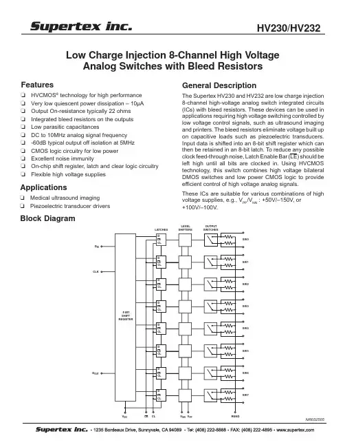
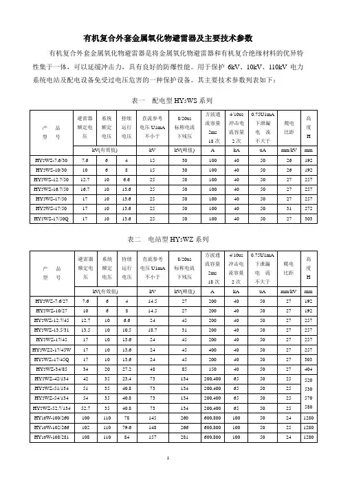
Low Charge Injection 8-Channel High VoltageAnalog Switches with Bleed ResistorsFeatures❏HVCMOS ® technology for high performance ❏Very low quiescent power dissipation – 10µA ❏Output On-resistance typically 22 ohms ❏Integrated bleed resistors on the outputs ❏Low parasitic capacitances❏DC to 10MHz analog signal frequency ❏-60dB typical output off isolation at 5MHz ❏CMOS logic circuitry for low power ❏Excellent noise immunity❏On-chip shift register, latch and clear logic circuitry ❏Flexible high voltage suppliesBlock DiagramD OUTD INCLKApplications❏Medical ultrasound imaging ❏Piezoelectric transducer driversGeneral DescriptionThe Supertex HV230 and HV232 are low charge injection 8-channel high-voltage analog switch integrated circuits (ICs) with bleed resistors. These devices can be used in applications requiring high voltage switching controlled by low voltage control signals, such as ultrasound imaging and printers. The bleed resistors eliminate voltage built up on capacitive loads such as piezoelectric transducers.Input data is shifted into an 8-bit shift register which can then be retained in an 8-bit latch. To reduce any possible clock feed-through noise, Latch Enable Bar (LE) should be left high until all bits are clocked in. Using HVCMOS technology, this switch combines high voltage bilateral DMOS switches and low power CMOS logic to provide efficient control of high voltage analog signals.These ICs are suitable for various combinations of high voltage supplies, e.g., V PP /V NN : +50V/–150V, or +100V/–100V.Ordering InformationAbsolute Maximum Ratings*V DD Logic power supply voltage -0.5V to +15VV PP - V NN Supply voltage 220VV PP Positive high voltage supply -0.5V to V NN +200VV NN Negative high voltage supply +0.5V to -200V Logic input voltages -0.5V to V DD +0.3VAnalog Signal RangeV NN to V PPPeak analog signal current/channel 3.0AStorage temperature -65°C to +150°CPower dissipation:28-lead PLCC 1.2W 48-lead TQFP 1.0W 26-lead TAPP 1.0W 26-lead µ-BGA1.0W*Absolute Maximum Ratings are those values beyond which damage to the device may occur. Functional operation under these condi-tions is not implied. Continuous operation of the device at the absolute rating level may affect device reliability. All voltages are referenced to device ground.Symbol ParameterValueV DD Logic power supply voltage 1, 3 4.5V to 13.2V V PP Positive high voltage supply 1, 340V to V NN + 200V V NN Negative high voltage supply 1, 3-40V to -160V V IH High-level input voltage V DD -1.5V to V DD V IL Low-level input voltage0V to 1.5VV SIG Analog signal voltage peak to peak V NN +10V to V PP -10V 2T AOperating free air-temperature0°C to 70°CNotes:1Power up/down sequence is arbitrary except GND must be powered-up first and powered-down last.2V SIG must be V NN - V SIG - V PP or floating during power up/down transistion.3Rise and fall times of power supplies V DD , V PP , and V NN should not be less than 1.0msec.Operating Conditions *Package Options28-Lead plastic chip carrier 48-Lead TQFP 26-lead TAPP26-lead µ-BGA Die HV232PJHV232FGHV232XHV230TA--HV232GA---V PP - V NN200V 200VHV230/232 Truth TableD0D1D2D3D4D5D6D7LE CL SW0SW1SW2SW3SW4SW5SW6SW7L L L OFFH L L ONL L L OFFH L L ONL L L OFFH L L ONL L L OFFH L L ONL L L OFFH L L ONL L L OFFH L L ONL L L OFFH L L ONL L L OFFH L L ONX X X X X X X X H L HOLD PREVIOUS STATEX X X X X X X X X H OFF OFF OFF OFF OFF OFF OFF OFFNotes:1.The eight switches operate independently.2.Serial data is clocked in on the L to H transition CLK.3.The switches go to a state retaining their present condition at the rising edge of LE. When LE islow the shift register data flows through the latch.4.D OUT is high when data in shift register 7 is high.5.Shift register clocking has no effect on the switch states if LE is H.6.The clear input overrides all other inputs.DC Characteristics (over recommended operating conditions unless otherwise noted)30263848I SIG = 5mAV PP = 40V,25222732I SIG = 200mA V NN = -160VSmall Signal Switch (ON)R ONS25222730ΩI SIG = 5mA V PP = 100V,Resistance18182427I SIG = 200mA V NN = -100V 23202530I SIG = 5mAV PP = 160V,22162527I SIG = 200mA V NN = -40V Small Signal Switch (ON)∆R ONS 205.02020%I SW = 5mA, V PP = 100V,Resistance Matching V NN = -100VLarge Signal Switch (ON)R ONL 15ΩV SIG = V PP - 10V, I SIG = 1A ResistanceOutput Switch Shunt R INT 203550K ΩOutput switch to R GND Resistance I RINT = 0.5mA Switch Off Leakage I SOL5.0 1.01015µA V SIG = V PP - 10V Per SwitchDC Offset Switch Off 300100300300mV No Load DC Offset Switch On 500100500500mV No Load Pos. HV Supply Current I PPQ 1050µA ALL SWs OFF Neg. HV Supply Current I NNQ -10-50µA ALL SWs OFFPos. HV Supply Current I PPQ 1050µA ALL SWs ON, I SW = 5mA Neg. HV Supply Current I NNQ-10-50µA ALL SWs ON, I SW = 5mA Switch Output 3.03.02.0 2.0A V SIG duty cycle - 0.1%Peak CurrentOutput Switch Frequencyf SW50KHzDuty Cycle = 50%6.57.08.0V PP = 40V,V NN = -160VI PP Supply CurrentI PP4.05.0 5.5mAV PP = 100V,V NN = -100V 4.0 5.0 5.5V PP = 160V,V NN = -40V 6.57.08.0V PP = 40V,V NN = -160VI NN Supply CurrentI NN4.05.0 5.5mAV PP = 100V,V NN = -100V 4.05.0 5.5V PP = 160V,V NN = -40VLogic Supply I DD 4.0 4.0 4.0mA f CLK = 5MHz, V DD = 5.0VAverage Current Logic SupplyI DDQ 101010µA Quiescent Current Data Out Source Current I SOR 0.450.450.700.40mA V OUT = V DD - 0.7V Data Out Sink Current I SINK 0.450.450.700.40mAV OUT = 0.7VLogic Input CapacitanceC IN101010pF0°C +25°C +70°C CharacteristicsSymUnits Test Conditions min maxmintyp*max min max50KHz Output Switching Frequency with no load*Typical values only for HV232AC Characteristics (over operating conditions V DD = 5V, unless otherwise noted)0°C +25°C+70°CCharacteristicsSym min maxmin typ*maxmin maxUnits Test Condi tionsSet Up Time Before LE Rises t SD 150150150ns Time Width of LEt WLE 150150150nsClock Delay Time to Data Out t DO 551506015070150ns Time Width of CLt WCL 150150150ns Set Up Time Data to Clock t SU 15158.020ns Hold Time Data from Clock t h 353535nsClock Freqf CLK 5.0 5.0 5.0MHz 50% duty cycle f DATA = f CLK /2Clock Rise and Fall Times t r , t f 1.0 1.0 1.0µs Turn On Time t ON 5.0 5.0 5.0µs V SIG = V PP -10V,R L = 10K ΩTurn Off Timet OFF5.0 5.0 5.0µsV SIG = V PP -10V,R L = 10K Ω202020V PP = 160V,V NN = -40VMaximum V SIG Slew Ratedv/dt202020V/nsV PP = 100V,V NN = -100V 202020V PP = 40V,V NN = -160VOff IsolationKO-30-30-33-30dB f = 5MHz,1K Ω//15pF load -58-58-58dB f = 5MHz,50Ω load Switch Crosstalk K CR -60-60-70-60dBf = 5MHz,50Ω load Output Switch Isolation I ID 300300300mA 300ns pulse width,Diode Current2.0% duty cycle Off Capacitance SW to GND C SG(OFF) 5.017 5.01217 5.017pF 0V, 1MHz On Capacitance SW to GNDC SG(ON)25502538502550pF0V, 1MHzAC Characteristics (over operating conditions V DD = 5V, unless otherwise noted)V PP = 40V, V NN = -160V, R L = 50ΩV PP = 100V, V NN = -100V, R L = 50ΩV PP = 160V, V NN = -40V, R L = 50Ω150150150150150150mVOutput Voltage Spike+25°C UnitsCharacteristics Sym Test Conditionsmin typ* max+V SPK-V SPK +V SPK -V SPK +V SPK -V SPK*Typical values only for HV232Electrical Characteristics*Typical values only for HV232HV230/232Test CircuitsSwitch OFF LeakageV PP–10VDC Offset ON/OFFV OUTT ON /T OFF T est CircuitV Isolation Diode Current V SIGCrosstalkK CR = 20LogOUT V INV IN Charge Injection V SIGV Q = 1000pF x ∆V OUTOutput Voltage SpikeOFF Isolation O OUT V INVHV230/232LE CLV PPV NN V DDRGNDD OUTD INCLKLogic Timing WaveformsD N - 1NN + 1D D OUT(TYP)CLRHV230/232Package OutlinesHV232 28-Pin J-Lead Pin Function PinFunction 1SW315N/C 2SW316D IN 3SW217CLK 4SW218LE 5SW119CL 6SW120D OUT 7SW021SW78SW022SW79N/C 23SW610V PP 24SW611R GND 25SW512V NN 26SW513GND 27SW414V DD28SW4HV232 48-Pin TQFP Pin Function 1SW52N/C 3SW44N/C 5SW46N/C 7N/C 8SW39N/C 10SW311N/C 12SW213N/C 14SW215N/C 16SW117N/C 18SW119N/C 20SW021N/C 22SW023N/C 24V PPPinFunction 25V NN 26N/C 27R GND 28GND 29V DD 30N/C 31N/C 32N/C 33D IN 34CLK 35LE 36CLR 37D OUT 38N/C 39SW740N/C 41SW742N/C 43SW644N/C 45SW646N/C 47SW548N/CPin ConfigurationsTop View28-Pin J-Lead Package123412131415161718262728Top View 48-Pin TQFPPin 1Pin 12HV230/232HV232GA Package Outline (µ-BGA)INDEXNotes:1.Dimensioning and tolerance per ASME Y14.5M-1994.2.Do not subject part to ultrasonic cleaning or intense UV.3.Contact ball position per JESD 95-1, SPP-010.4.Units are in millimeters.HV230/232µ-BGA Function TableBall Location FunctionA4SW1C3SW2C4SW1C5SW0C6V PPC7V NND1SW3D3SW3D4SW2D5SW0D6R GNDD7GNDD9V DDE1SW4E3SW4E4SW5E5SW7E6LEE7CLKE9D INF3SW5F4SW6F5SW7F6D OUTF7CLRH4SW6HV230/232123456789101112131415161718Pad connections are on the backside of the packageBottom ViewDimensions are in mmPin ConfigurationPackage DimensionsPad Diagram#n i P n o i t c n u F #n i P n o i t c n u F 14W S 41V D D 23W S 51D N I 33W S 61K L C 42W S 71r a b E L 52W S 81R L C 61W S 91D T U O 71W S 027W S 80W S 127W S 90W S 226W S 01V P P 326W S 11V N N 425W S 21R D N G 525W S 31DN G 624W S 元器件交易网。
韩国韩荣数码温度控制器|光电传感器|旋转编码器|接近传感器|计数器|按钮开关|蜂鸣器|信号灯温度控制器是利用感温液体热胀冷缩及液体不可压缩的原理而实现自动调节。
当控制温度升高时感温液体膨胀产生的推力将热媒关小,以降低输出温度;当控制温度降低时感温液体收缩,在复位装置的作用下将热媒开大,以提高输出温度,从而使被控制的温度达到和保持在所设定的温度范围内。
深圳市凯斯机电应用技术XXX(bbb://aaacase-tradeaaa)作为韩国韩荣系列数码温控器华南区的代理商,可以为您提供各种型号,各种规格,各种用途的数码温度控制器,专用温度控制器,温度控制器,普通温度控制器。
韩国韩荣温控器产品包括:可编程温度.湿度控制器、PID 温度控制器、一般型温度控制器、专用温度控制器、温度指示器、温度控制器的周边机器。
可编程温度.湿度控制器:可编程温度.湿度控制器|可编程温度控制器A:可编程温度.湿度控制器:TH500系列可编程温度、湿度控制器:适用触感面板的彩色LCD画面、300模式(总6000段)、接点输入(D.I)8点,数码输出(D.O)20点、基本搭载通信功能(RS232及RS485/422)。
测定范围:温度:-100.0 ~ 200.0 °C、0.000 ~ 5.000 V ( -100.0 ~ 200.0 °C) 。
湿度:-100.0 ~ 200.0 °C ( 0.0 ~ 100.0 % RH ) 、0.000 ~ 5.000 V ( 0.0 ~ 100.0 % RH ) 。
指示精度:温度( ± 0.1 % of F.S ) 、湿度( ± 1 % of F.S )。
取样周期:温/ 湿度500 ms 。
TH300系列可编程温度、湿度控制器:应用触摸屏的彩色LCD画面、300模式(共6000段) 、接点输入(D.I)4点,数码输出(D.O)12点、通讯功能(RS232及RS485/422) 根据型号选择。