组成第五章答案2010版本
- 格式:doc
- 大小:1.12 MB
- 文档页数:14
5.4 教材习题解答1.如何区别存储器和寄存器?两者是一回事的说法对吗?解:存储器和寄存器不是一回事。
存储器在CPU 的外边,专门用来存放程序和数据,访问存储器的速度较慢。
寄存器属于CPU 的一部分,访问寄存器的速度很快。
2.存储器的主要功能是什么?为什么要把存储系统分成若干个不同层次?主要有哪些层次?解:存储器的主要功能是用来保存程序和数据。
存储系统是由几个容量、速度和价存储系统和结构第5章1 29 格各不相同的存储器用硬件、软件、硬件与软件相结合的方法连接起来的系统。
把存储系统分成若干个不同层次的目的是为了解决存储容量、存取速度和价格之间的矛盾。
由高速缓冲存储器、主存储器、辅助存储器构成的三级存储系统可以分为两个层次,其中高速缓存和主存间称为Cache -主存存储层次(Cache 存储系统)主存和辅存间称为主存—辅存存储层次(虚拟存储系统)。
3.什么是半导体存储器?它有什么特点?解:采用半导体器件制造的存储器,主要有MOS 型存储器和双极型存储器两大类。
半导体存储器具有容量大、速度快、体积小、可靠性高等特点。
半导体随机存储器存储的信息会因为断电而丢失。
4. SRAM记忆单元电路的工作原理是什么?它和DRAM 记忆单元电路相比有何异同点?解:SRAM记忆单元由6个MOS管组成,利用双稳态触发器来存储信息,可以对其进行读或写,只要电源不断电,信息将可保留。
DRAM 记忆单元可以由4 个和单个MOS 管组成,利用栅极电容存储信息,需要定时刷新。
5.动态RAM为什么要刷新?一般有几种刷新方式?各有什么优缺点?解:DRAM 记忆单元是通过栅极电容上存储的电荷来暂存信息的,由于电容上的电荷会随着时间的推移被逐渐泄放掉,因此每隔一定的时间必须向栅极电容补充一次电荷,这个过程就叫做刷新。
常见的刷新方式有集中式、分散式和异步式3 种。
集中方式的特点是读写操作时不受刷新工作的影响,系统的存取速度比较高;但有死区,而且存储容量越大,死区就越长。

第五章PowerPoint20101.【单选】单击PowerPoint 2010“文件”选项卡下的“最近所用文件”命令,所显示的文件名是A. 正在使用的文件名B. 正在打印的文件名C. 扩展名为PPTX的文件名D. 最近被PowerPoint软件处理过的文件名正确答案是:D2.【单选】PowerPoint的幻灯片可以:A. 在计算机屏幕上放映B. 打印成幻灯片使用C. 在投影仪上放映D. 以上三种均可以完成正确答案是:D3.【单选】在幻灯片浏览视图中,可进行什么操作:A. 移动幻灯片B. 为幻灯片中的文字设置颜色C. 为幻灯片设置项目符号D. 向幻灯片中插入图表正确答案是:A4.【单选】在以下哪一种母版中插入徽标可以使其在每张幻灯片上的位置自动保持相同?A. 讲义母版。
B. 幻灯片母版。
C. 标题母版。
D. 备注母版。
正确答案是:B5.【单选】具有将多个幻灯片显示于窗口中的Powerpoint 视图是:A. 幻灯片浏览视图B. 幻灯片放映视图C. 普通视图D. 幻灯片视图正确答案是:A6.【单选】如果对一张幻灯片使用系统提供的版式,对其中各个对象的占位符___A. 能用具体内容去替换,不可删除B. 能移动位置,也不能改变格式C. 可以删除不用,也可以在幻灯片中插入新的对象D. 可以删除不用,但不能在幻灯片中插入新的对象正确答案是:7.【单选】PowerPoint 2010演示文稿的扩展名是()。
A. .pptB. .pptxC. .xslxD. .docx正确答案是:B8.【单选】幻灯片中占位符的作用是A. 表示文本的长度B. 限制插入对象的数量C. 表示图形的大小D. 为文本、图形预留位置正确答案是:D9.【单选】关于保存和另存为说法正确的是A. 在文件第一次保存的时候两者功能相同B. 另存为是将文件再保存一份,但不可以重新给文件命名C. 用另存为保存的文件不能与原文件同名D. 两者在任何情况下都相同正确答案是:A10.【单选】在Powerpoint中,为所有幻灯片设置统一的特有的外观风格,应运用哪种A. 母版B. 自动版式C. 配色方案D. 联机协作正确答案是:A11.【单选】在PowerPoint 2010中,下列关于幻灯片版式说法正确的是____A. 在“标题和内容”版式中,没有“剪贴画”占位符B. 剪贴画只能插入到空白版式中C. 任何版式中都可以插入剪贴画D. 剪贴画只能插入到有“剪贴画”占位符的版式中正确答案是:C12.【单选】在PowerPoint2010 中,以下说法正确的是A. 没有标题文字,只有图片或其他对象的幻灯片,在大纲中是不反映出来的B. 大纲视图窗格是可以用来编辑修改幻灯片中对象的位置C. 备注页视图中的幻灯片是一张图片,可以被拖动D. 对应于四种视图,PowerPoint有四种母版正确答案是:A13.【单选】若将PowerPoint文档保存只能播放不能编辑的演示文稿,操作方法是A. 保存对话框中的保存类型选择为"PDF"格式B. 保存对话框中的保存类型选择为"网页"C. 保存对话框中的保存类型选择为"模板"D. 保存(或另存为)对话框中的保存类型选择为"Powerpoint放映"正确答案是:D14.【单选】在PowePoint 2010中,大纲工具栏无法实现的功能是A. 升级B. 降级C. 摘要D. 版式正确答案是:D15.【单选】在PPT的打印预览视图中,下面说法正确的是A. 可以对文字进行编辑B. 不可设置幻灯片的切换效果C. 能将幻灯片加边框D. 不能修改显示比例正确答案是:C16.【单选】在PowerPoint 2010中,不可以插入__C____文件(选项中给出的是不同类型文件的扩展名)A. AviB. WavC. ExeD. Bmp(或Png)正确答案是:C17.【单选】在PowerPoint2010中,对于已创建的多媒体演示文档可以用______命令转移到其他未安装PowerPoint的机器上放映。
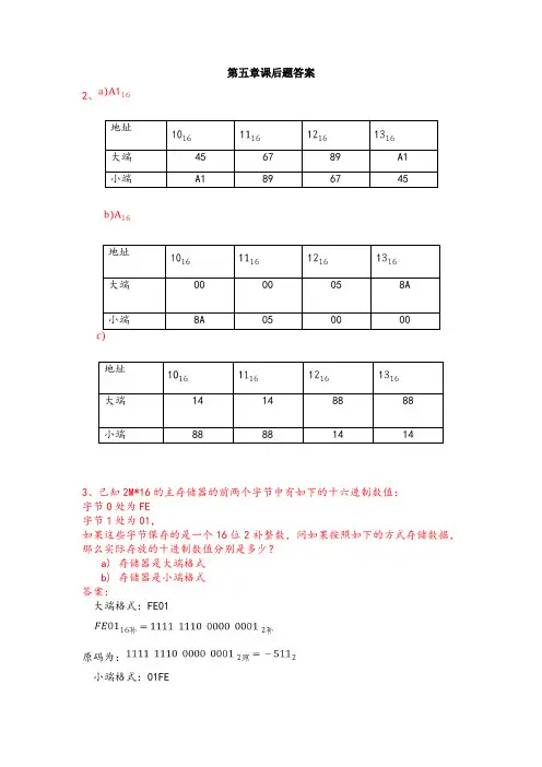
第五章课后题答案2、3、已知2M*16的主存储器的前两个字节中有如下的十六进制数值: 字节0处为FE 字节1处为01,如果这些字节保存的是一个16位2补整数,问如果按照如下的方式存储数据,那么实际存放的十进制数值分别是多少?a) 存储器是大端格式 b) 存储器是小端格式 答案:大端格式:FE01原码为:小端格式:01FE原码为:8、将下列表达式由中缀表示法变换成反向逆波兰(后缀)表示法:a)X*Y+W*Z+V*Ub)W*X+W*(U*V+Z)c)(W*(X+Y*(U*V)))/(U*(X+Y))答案:a)X*Y + W*Z + V*U=>XY* + WZ* + VU*=>XY* WZ* + + VU*=>XY* WZ*+VU*+b)W*X + W*(U*V + Z)=>WX* + W*(UV* + Z)=>WX* + W*(UV*Z +)=>WX* + WUV*Z + *=>WX* WUV*Z+*+c)(W*(X + Y*(U*V)))/(U*(X + Y))=>(W*(X + Y*(UV*)))/(U*(XY+))=>(W*(X + YUV**))/UXY+*=>(W*(XYUV**+))/UXY+*=>(WXYUV**+*)/UXY+*=>WXYUV**+*UXY+*/9、将下列反向逆波兰式(后缀)表示法转换成中缀表示法:a)WXYZ-+*=>WXY-Z+*=>WX+Y-Z*=>W*(X+Y-Z)b)UVWXYZ+*+*+=>UVWXY+Z*+*+=>UVWX*(Y+Z)+*+=>UVW+X*(Y+Z)*+=>UV*(W+X*(Y+Z))+=>U+V*(W+X*(Y+Z))c)XYZ+VW-*Z++=>XY+ZV-W*Z++=>X(Y+Z)*(V-W)Z++=>X(Y+Z)*(V-W)+Z+=>X+((Y+Z)*(V-W)+Z)11、如果某台计算机的指令格式为:指令的长度共11位,而地址域的大小占4位,试证明采用这种指令格式的计算机是否可能有如下的指令形式,并验证你的答案:5个二地址指令45个一地址指令32个零地址指令000 xxxx xxxx001 xxxx xxxx010 xxxx xxxx 5个二地址指令011 xxxx xxxx100 xxxx xxxx45个一地址指令:101 0000 xxxx 16条101 1111 xxxx110 0000 xxxx 16条110 1111 xxxx111 0000 xxxx13条111 1100 xxxx32个0地址指令111 11100000 16条111 11101111111 1111 0000 16条111 1111 1111b)假如某台采用上述指令格式的计算机体系结构,并设计了6个2地址指令和24个0地址指令,试问可以在该指令系统中添加的1地址指令的最大数目是多少?000 xxxx xxxx 6个101 xxxx xxxx0地址指令: 24=3*8111 1111 1000 8个 111 1111 1111111 1111 0000 8个 111 1111 0111111 1110 1000 8个111 1110 1111一地址前三位110:110 0000 xxxx 共16条 110 1111 xxxx 一地址前三位111:111 0000 xxxx 共14条 111 1101 xxxx ∴最大数目是3013、如果有指令Load 1000,并且已知存储器和寄存器RI 中包含如下数值:存储器 R11000110012001300 1400假设R1隐含在变址寻址方式中,试确定指令嵌入到累加器中实际数值,并填写值1000直接装入AC 中。
第5章柴油机燃料供给系统5-1答:整个系统由低压油路(柴油箱、输油泵、柴油滤清器及低压油管)、高压油路(喷油泵、高压油管、喷油器)和调节系统(离心式调速器、自动供油提前器)组成。
5-2答:(1)基本结构柱塞式喷油泵由分泵、油量调节机构、驱动机构、泵体4部分组成。
分泵的结构是由柱塞、柱塞套筒、柱塞回位弹簧、弹簧座、出油阀、出油阀座、出油阀弹簧、减容器及出油阀压紧螺母等零件组成。
油量调节机构有拨叉式和齿杆式两种。
拨叉式油量调节机构是由调节臂、调节叉(拨叉)及供油拉杆组成。
齿杆式油量调节机构是由齿杆、齿扇和传动套等组成。
喷油泵的驱动机构由喷油泵的凸轮轴和滚轮体等传动件组成。
(2)泵油原理燃油自低压油腔经油孔被吸入并充满泵腔。
在柱塞自下止点上移的过程中,起初有一部分燃油被从泵腔挤回低压油腔,直到柱塞上部的圆柱面将两个油孔完全封闭时为止。
此后,柱塞继续上升,柱塞上部的燃油压力顿时增加到足以克服出油阀弹簧的作用力,出油阀即开始上升。
当出油阀上的圆柱形环带离开出油阀座时,高压燃油便自泵腔通过高压油管流向喷油器。
当柱塞再上移到斜槽同油孔开始接通时,于是泵腔内的燃油便经柱塞中央的孔道、斜槽和油孔流向低压油腔,这时泵腔中油压迅速下降,出油阀在弹簧压力作用下立即回位,喷油泵供油即行停止。
5-3答:(1)径向压缩式分配泵1)结构径向压缩式分配泵的结构主要由高压泵头,它由旋转部分(包括分配转子、柱塞、滚柱、滚柱座、)和固定部分(分配套筒、内凸轮)组成。
2)工作原理分配转子转动时,推动滚柱座、滚柱和柱塞绕其轴线转动。
由于固定的凸轮的凸起使对置的柱塞被推向转子中心,柴油产生高压,此时分配孔正好与分配筒上相应的出油孔对上,高压柴油被送到喷油器。
(2)轴向压缩式分配泵1)结构它主要有分配柱塞、平面凸轮盘、柱塞套、调速器张力杠杆、断油阀及液压式喷油提前器等组成。
2)工作过程(1)进油过程。
当平面凸轮盘转动列其凹下部分与滚轮接触时,分配柱塞向左移动,低压柴油经进油道、柱塞套上的进油孔(此时断油阀已打开)被吸入柱塞腔和中心油孔内。

计算机组成原理第五章部分课后题答案5.1 I/O设备有哪些编址方式,各有何特点?常用的I/O编址方式有两种:I/O与内存统一编址和I/O独立编址·I/O与内存统一编址方式的I/O地址采用与主存单元地址完全一样的格式,I/O设备与主存占用同一个地址空间,CPU可像访问主存一样访问I/O设备,不需要安排专门的I/O指令。
·I/O独立编址方式时机器为I/O设备专门安排一套完全不同于主存地址格式的地址编码,此时I/O地址与主存地址是两个独立的空间,CPU需要通过专门的I/O指令来访问I/O地址空间。
5.3 I/O设备与主机交换信息时,共有哪几种控制方式?简述它们的特点。
·程序直接控制方式:也称查询方式,采用该方式,数据在CPU和外设间的传送完全靠计算机程序控制,CPU的操作和外围设备操作同步,硬件结构简单,但由于外部设备动作慢,浪费CPU时间多,系统效率低。
·程序中断方式:外设备准备就绪后中断方式猪肚通知CPU,在CPU相应I/O设备的中断请求后,在暂停现行程序的执行,转为I/O 设备服务可明显提高CPU的利用率,在一定程度上实现了主机和I/O设备的并行工作,但硬件结构负载,服务开销时间大·DMA方式与中断方式一样,实现了主机和I/O设备的并行工作,由于DMA 方式直接依靠硬件实现贮存与I/O设备之间的数据传送,传送期间不需要CPU程序干预,CPU可继续执行原来的程序,因此CPU利用率和系统效率比中断方式更高,但DMA方式的硬件结构更为复杂。
5.4 比较程序查询方式、程序中断方式和DMA方式对CPU工作效率的影响。
·程序查询方式:主要用于CPU不太忙且传送速度不高的情况下。
无条件传送方式作为查询方式的一个特例,主要用于对简单I/O设备的控制或CPU明确知道外设所处状态的情况下。
·中断方式:主要用于CPU的任务比较忙的情况下,尤其适合实时控制和紧急事件的处理· DMA方式(直接存储器存取方式):主要用于高速外设进行大批量数据传送的场合。
第五章部分习题参考答案【5-10】一个1K * 8的存储芯片需要多少根地址线,数据输入输出线?解:1024 = 10 根。
由于一次可读写8位数据,所以需要8根数据输入输出线。
n = log2【5-11】某计算机字长32位,存储容量64KB,按字编址的寻址范围是多少?若主存以字节编址,试画出主存字地址和字节地址的分配情况?解:因为字长32位,所以64KB = 16KW,要表示16K个存储单元,需要14根地址线。
所以按字编址的寻址范围是0000H ~ 3FFFH 。
若按字节编址,假设采用PC机常用的小端方案,则主存示意图如下:【5-13】现有1024×1的存储芯片,若用它组成容量为16K×8的存储器。
试求:(1)实现该存储器所需芯片数量(2)若将这些芯片分装在若干块板上,每块板的容量是4K×8,该存储器所需的地址线的总位数是多少?其中几位用于选板?几位用于选片?几位用作片内地址?解:(1)需要16组来构成16K,共需芯片16×8 = 128片(2)需要的地址线总位数是14位。
因为共需4块板,所以2位用来选板,板内地址12位,片内地址10位。
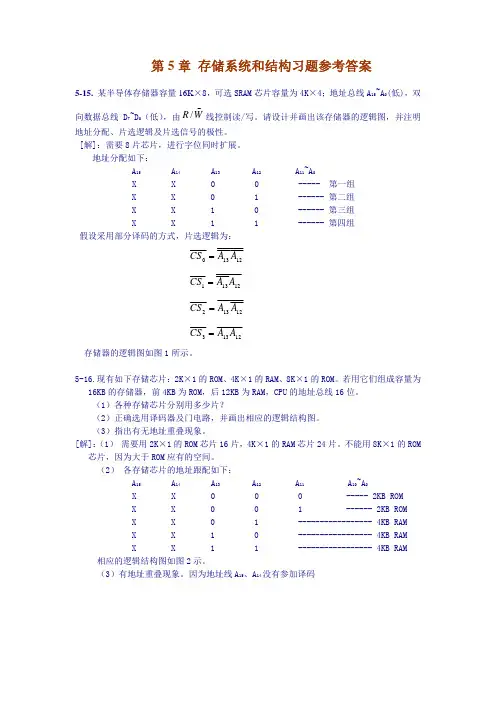
每块板的结构如下图4块板共同组成16K×8存储器的结构图【5-15】某半导体存储器容量16K×8,可选SRAM芯片的容量为4K ×4;地址总线A15~A0(A0为最低位),双向数据总线D7~D0,由R/W线控制读写。
设计并画出该存储器的逻辑图,并注明地址分配、片选逻辑和片选信号的极性。
解:注:采用全译码方式方案4组不同的4K的RAM芯片。
可以写出片选逻辑表达式【5-17】用容量为16K×1的DRAM芯片构成64KB的存储器(1)画出该存储器的结构框图(2)设存储器的读写周期均为0.5微秒,CPU在1微秒内至少要访存一次,试问采用哪种刷新方式比较合理?相邻两行之间的刷新间隔是多少?对全部存储单元刷新一遍所需的实际刷新时间是多少?解:(1)结构框图如下(若看不清可以从”视图”菜单中调整显示比例)(2)由于存储器芯片规格为16K×1,所以,其芯片内部的存储矩阵是128×128的存储矩阵。
计算机组成与设计:《计算机组成与设计》是2010年机械工业出版社出版的图书,作者是帕特森(DavidA.Patterson)。
该书讲述的是采用了一个MIPS 处理器来展示计算机硬件技术、流水线、存储器的层次结构以及I/O 等基本功能。
此外,该书还包括一些关于x86架构的介绍。
内容简介:这本最畅销的计算机组成书籍经过全面更新,关注现今发生在计算机体系结构领域的革命性变革:从单处理器发展到多核微处理器。
此外,出版这本书的ARM版是为了强调嵌入式系统对于全亚洲计算行业的重要性,并采用ARM处理器来讨论实际计算机的指令集和算术运算。
因为ARM是用于嵌入式设备的最流行的指令集架构,而全世界每年约销售40亿个嵌入式设备。
采用ARMv6(ARM 11系列)为主要架构来展示指令系统和计算机算术运算的基本功能。
覆盖从串行计算到并行计算的革命性变革,新增了关于并行化的一章,并且每章中还有一些强调并行硬件和软件主题的小节。
新增一个由NVIDIA的首席科学家和架构主管撰写的附录,介绍了现代GPU的出现和重要性,首次详细描述了这个针对可视计算进行了优化的高度并行化、多线程、多核的处理器。
描述一种度量多核性能的独特方法——“Roofline model”,自带benchmark测试和分析AMD Opteron X4、Intel Xeo 5000、Sun Ultra SPARC T2和IBM Cell的性能。
涵盖了一些关于闪存和虚拟机的新内容。
提供了大量富有启发性的练习题,内容达200多页。
将AMD Opteron X4和Intel Nehalem作为贯穿《计算机组成与设计:硬件/软件接口(英文版·第4版·ARM版)》的实例。
用SPEC CPU2006组件更新了所有处理器性能实例。
图书目录:1 Computer Abstractions and Technology1.1 Introduction1.2 BelowYour Program1.3 Under the Covers1.4 Performance1.5 The Power Wall1.6 The Sea Change: The Switch from Uniprocessors to Multiprocessors1.7 Real Stuff: Manufacturing and Benchmarking the AMD Opteron X41.8 Fallacies and Pitfalls1.9 Concluding Remarks1.10 Historical Perspective and Further Reading1.11 Exercises2 Instructions: Language of the Computer2.1 Introduction2.2 Operations of the Computer Hardware2.3 Operands of the Computer Hardware2.4 Signed and Unsigned Numbers2.5 Representing Instructions in the Computer2.6 Logical Operations2.7 Instructions for Making Decisions2.8 Supporting Procedures in Computer Hardware2.9 Communicating with People2.10 ARM Addressing for 32-Bit Immediates and More Complex Addressing Modes2.11 Parallelism and Instructions: Synchronization2.12 Translating and Starting a Program2.13 A C Sort Example to Put lt AU Together2.14 Arrays versus Pointers2.15 Advanced Material: Compiling C and Interpreting Java2.16 Real Stuff." MIPS Instructions2.17 Real Stuff: x86 Instructions2.18 Fallacies and Pitfalls2.19 Conduding Remarks2.20 Historical Perspective and Further Reading2.21 Exercises3 Arithmetic for Computers3.1 Introduction3.2 Addition and Subtraction3.3 Multiplication3.4 Division3.5 Floating Point3.6 Parallelism and Computer Arithmetic: Associativity 3.7 Real Stuff: Floating Point in the x863.8 Fallacies and Pitfalls3.9 Concluding Remarks3.10 Historical Perspective and Further Reading3.11 Exercises4 The Processor4.1 Introduction4.2 Logic Design Conventions4.3 Building a Datapath4.4 A Simple Implementation Scheme4.5 An Overview of Pipelining4.6 Pipelined Datapath and Control4.7 Data Hazards: Forwarding versus Stalling4.8 Control Hazards4.9 Exceptions4.10 Parallelism and Advanced Instruction-Level Parallelism4.11 Real Stuff: theAMD OpteronX4 (Barcelona)Pipeline4.12 Advanced Topic: an Introduction to Digital Design Using a Hardware Design Language to Describe and Model a Pipelineand More Pipelining Illustrations4.13 Fallacies and Pitfalls4.14 Concluding Remarks4.15 Historical Perspective and Further Reading4.16 Exercises5 Large and Fast: Exploiting Memory Hierarchy5.1 Introduction5.2 The Basics of Caches5.3 Measuring and Improving Cache Performance5.4 Virtual Memory5.5 A Common Framework for Memory Hierarchies5.6 Virtual Machines5.7 Using a Finite-State Machine to Control a Simple Cache5.8 Parallelism and Memory Hierarchies: Cache Coherence5.9 Advanced Material: Implementing Cache Controllers5.10 Real Stuff: the AMD Opteron X4 (Barcelona)and Intel NehalemMemory Hierarchies5.11 Fallacies and Pitfalls5.12 Concluding Remarks5.13 Historical Perspective and Further Reading5.14 Exercises6 Storage and Other I/0 Topics6.1 Introduction6.2 Dependability, Reliability, and Availability6.3 Disk Storage6.4 Flash Storage6.5 Connecting Processors, Memory, and I/O Devices6.6 Interfacing I/O Devices to the Processor, Memory, andOperating System6.7 I/O Performance Measures: Examples from Disk and File Systems6.8 Designing an I/O System6.9 Parallelism and I/O: Redundant Arrays of Inexpensive Disks6.10 Real Stuff: Sun Fire x4150 Server6.11 Advanced Topics: Networks6.12 Fallacies and Pitfalls6.13 Concluding Remarks6.14 Historical Perspective and Further Reading6.15 Exercises7 Multicores, Multiprocessors, and Clusters7.1 Introduction7.2 The Difficulty of Creating Parallel Processing Programs7.3 Shared Memory Multiprocessors7.4 Clusters and Other Message-Passing Multiprocessors7.5 Hardware Multithreading 637.6 SISD,MIMD,SIMD,SPMD,and Vector7.7 Introduction to Graphics Processing Units7.8 Introduction to Multiprocessor Network Topologies7.9 Multiprocessor Benchmarks7.10 Roofline:A Simple Performance Model7.11 Real Stuff:Benchmarking Four Multicores Using theRooflineMudd7.12 Fallacies and Pitfalls7.13 Concluding Remarks7.14 Historical Perspective and Further Reading7.15 ExercisesInuexC D-ROM CONTENTA Graphics and Computing GPUSA.1 IntroductionA.2 GPU System ArchitecturesA.3 Scalable Parallelism-Programming GPUSA.4 Multithreaded Multiprocessor ArchitectureA.5 Paralld Memory System G.6 Floating PointA.6 Floating Point ArithmeticA.7 Real Stuff:The NVIDIA GeForce 8800A.8 Real Stuff:MappingApplications to GPUsA.9 Fallacies and PitflaUsA.10 Conduding RemarksA.1l HistoricalPerspectiveandFurtherReadingB1 ARM and Thumb Assembler InstructionsB1.1 Using This AppendixB1.2 SyntaxB1.3 Alphabetical List ofARM and Thumb Instructions B1.4 ARM Asembler Quick ReferenceB1.5 GNU Assembler Quick ReferenceB2 ARM and Thumb Instruction EncodingsB3 Intruction Cycle TimingsC The Basics of Logic DesignD Mapping Control to HardwareADVANCED CONTENTHISTORICAL PERSPECTIVES & FURTHER READINGTUTORIALSSOFTWARE作者简介:David A.Patterson,加州大学伯克利分校计算机科学系教授。
Chapter 5 Solutions S-35.15.1.1 45.1.2 I, J5.1.3 A[I][J]5.1.4 3596 ϭ 8 ϫ 800/4 ϫ 2Ϫ8ϫ8/4 ϩ 8000/45.1.5 I, J5.1.6 A(J, I)5.25.2.130000 001103M1801011 0100114M430010 1011211M20000 001002M1911011 11111115M880101 100058M1901011 11101114M140000 1110014M1811011 0101115M440010 1100212M1861011 10101110M2531111 11011513M5.2.230000 001101M1801011 0100112M430010 101125M20000 001001H1911011 1111117M880101 100054M1901011 1110117H140000 111007M1811011 0101112H440010 110026M1861011 1010115M2531111 1101156MS-4 ChapterSolutions55.2.330000 001103M1M0M1801011 0100224M2M1M430010 101153M1M0M20000 001002M1M0M1911011 1111237M3M1M880101 1000110M0M0M1901011 1110236M3H1H140000 111016M3M1M1811011 0101225M2H1M440010 110054M2M1M1861011 1010232M1M0M2531111 1101315M2M1MCache 1 miss rate ϭ 100%Cache 1 total cycles ϭ 12 ϫ 25 ϩ 12 ϫ 2 ϭ 324Cache 2 miss rate ϭ 10/12 ϭ 83%Cache 2 total cycles ϭ 10 ϫ 25 ϩ 12 ϫ 3 ϭ 286Cache 3 miss rate ϭ 11/12 ϭ 92%Cache 3 total cycles ϭ 11 ϫ 25 ϩ 12 ϫ 5 ϭ 335Cache 2 provides the best performance.5.2.4 First we must compute the number of cache blocks in the initial cacheconfi guration. For this, we divide 32 KiB by 4 (for the number of bytes per word)and again by 2 (for the number of words per block). Th is gives us 4096 blocks anda resulting index fi eld width of 12 bits. We also have a word off set size of 1 bit and abyte off set size of 2 bits. Th is gives us a tag fi eld size of 32 Ϫ 15 ϭ 17 bits. Th ese tagbits, along with one valid bit per block, will require 18 ϫ 4096 ϭ 73728 bits or 9216bytes. Th e total cache size is thus 9216 ϩ 32768 ϭ 41984 bytes.Th e total cache size can be generalized tototalsize ϭ datasize ϩ (validbitsize ϩ tagsize) ϫ blockstotalsize ϭ 41984datasize ϭ blocks ϫ blocksize ϫ wordsizewordsize ϭ 4tagsize ϭ 32 Ϫ log2(blocks) Ϫ log2(blocksize) Ϫ log2(wordsize)validbitsize ϭ 1Chapter 5 Solutions S-5 Increasing from 2-word blocks to 16-word blocks will reduce the tag size from17 bits to 14 bits.In order to determine the number of blocks, we solve the inequality:41984 Ͻϭ 64 ϫ blocks ϩ 15 ϫ blocksSolving this inequality gives us 531 blocks, and rounding to the next power oftwo gives us a 1024-block cache.Th e larger block size may require an increased hit time and an increased misspenalty than the original cache. Th e fewer number of blocks may cause a higherconfl ict miss rate than the original cache.5.2.5 Associative caches are designed to reduce the rate of confl ict misses. Assuch, a sequence of read requests with the same 12-bit index fi eld but a diff erenttag fi eld will generate many misses. For the cache described above, the sequence0, 32768, 0, 32768, 0, 32768, …, would miss on every access, while a 2-way setassociate cache with LRU replacement, even one with a signifi cantly smaller overallcapacity, would hit on every access aft er the fi rst two.5.2.6 Y es, it is possible to use this function to index the cache. However,information about the fi ve bits is lost because the bits are XOR’d, so you mustinclude more tag bits to identify the address in the cache.5.35.3.1 85.3.2 325.3.3 1ϩ (22/8/32) ϭ 1.0865.3.4 35.3.5 0.255.3.6 ϽIndex, tag, dataϾϽ0000012, 00012, mem[1024]ϾϽ0000012, 00112, mem[16]ϾϽ0010112, 00002, mem[176]ϾϽ0010002, 00102, mem[2176]ϾϽ0011102, 00002, mem[224]ϾϽ0010102, 00002, mem[160]ϾS-6 ChapterSolutions55.45.4.1 Th e L1 cache has a low write miss penalty while the L2 cache has a highwrite miss penalty. A write buff er between the L1 and L2 cache would hide thewrite miss latency of the L2 cache. Th e L2 cache would benefi t from write buff erswhen replacing a dirty block, since the new block would be read in before the dirtyblock is physically written to memory.5.4.2 On an L1 write miss, the word is written directly to L2 without bringingits block into the L1 cache. If this results in an L2 miss, its block must be broughtinto the L2 cache, possibly replacing a dirty block which must fi rst be written tomemory.5.4.3 Aft er an L1 write miss, the block will reside in L2 but not in L1. A subsequentread miss on the same block will require that the block in L2 be written back tomemory, transferred to L1, and invalidated in L2.5.4.4 One in four instructions is a data read, one in ten instructions is a datawrite. For a CPI of 2, there are 0.5 instruction accesses per cycle, 12.5% of cycleswill require a data read, and 5% of cycles will require a data write.Th e instruction bandwidth is thus (0.0030 ϫ 64) ϫ 0.5 ϭ 0.096 bytes/cycle. Th edata read bandwidth is thus 0.02 ϫ (0.13ϩ0.050) ϫ 64 ϭ 0.23 bytes/cycle. Th etotal read bandwidth requirement is 0.33 bytes/cycle. Th e data write bandwidthrequirement is 0.05 ϫ 4 ϭ 0.2 bytes/cycle.5.4.5 Th e instruction and data read bandwidth requirement is the same as in5.4.4. Th e data write bandwidth requirement becomes 0.02 ϫ 0.30 ϫ (0.13ϩ0.050)ϫ 64 ϭ 0.069 bytes/cycle.5.4.6 For CPIϭ1.5 the instruction throughput becomes 1/1.5 ϭ 0.67 instructionsper cycle. Th e data read frequency becomes 0.25 / 1.5 ϭ 0.17 and the write frequencybecomes 0.10 / 1.5 ϭ 0.067.Th e instruction bandwidth is (0.0030 ϫ 64) ϫ 0.67 ϭ 0.13 bytes/cycle.For the write-through cache, the data read bandwidth is 0.02 ϫ (0.17 ϩ0.067) ϫ64 ϭ 0.22 bytes/cycle. Th e total read bandwidth is 0.35 bytes/cycle. Th e data writebandwidth is 0.067 ϫ 4 ϭ 0.27 bytes/cycle.For the write-back cache, the data write bandwidth becomes 0.02 ϫ 0.30 ϫ(0.17ϩ0.067) ϫ 64 ϭ 0.091 bytes/cycle.Address041613223216010243014031001802180Line ID001814100191118Hit/miss M H M M M M M H H M M MReplace N N N N N N Y N N Y N YChapter 5 Solutions S-75.55.5.1 Assuming the addresses given as byte addresses, each group of 16 accesseswill map to the same 32-byte block so the cache will have a miss rate of 1/16. Allmisses are compulsory misses. Th e miss rate is not sensitive to the size of the cacheor the size of the working set. It is, however, sensitive to the access pattern andblock size.5.5.2 Th e miss rates are 1/8, 1/32, and 1/64, respectively. Th e workload isexploiting temporal locality.5.5.3 In this case the miss rate is 0.5.5.4 AMAT for B ϭ 8: 0.040 ϫ (20 ϫ 8) ϭ6.40AMAT for B ϭ 16: 0.030 ϫ (20 ϫ 16) ϭ 9.60AMAT for B ϭ 32: 0.020 ϫ (20 ϫ 32) ϭ 12.80AMAT for B ϭ 64: 0.015 ϫ (20 ϫ 64) ϭ 19.20AMAT for B ϭ 128: 0.010 ϫ (20 ϫ 128) ϭ 25.60B ϭ 8 is optimal.5.5.5 AMAT for B ϭ 8: 0.040 ϫ (24 ϩ 8) ϭ 1.28AMAT for B ϭ 16: 0.030 ϫ (24 ϩ 16) ϭ 1.20AMAT for B ϭ 32: 0.020 ϫ (24 ϩ 32) ϭ 1.12AMAT for B ϭ 64: 0.015 ϫ (24 ϩ 64) ϭ 1.32AMAT for B ϭ 128: 0.010 ϫ (24 ϩ 128) ϭ 1.52B ϭ 32 is optimal.5.5.6 Bϭ1285.65.6.1P1 1.52 GHzP2 1.11 GHz5.6.2P1 6.31 ns9.56 cyclesP2 5.11 ns 5.68 cycles5.6.3P112.64 CPI8.34 ns per instP27.36 CPI 6.63 ns per instS-8 Chapter5Solutions5.6.46.50 ns9.85 cycles Worse5.6.513.045.6.6 P1 AMAT ϭ 0.66 ns ϩ 0.08 ϫ 70 ns ϭ 6.26 nsP2 AMAT ϭ 0.90 ns ϩ 0.06 ϫ (5.62 ns ϩ 0.95 ϫ 70 ns) ϭ 5.23 nsFor P1 to match P2’s performance:5.23 ϭ 0.66 ns ϩ MR ϫ 70 nsMR ϭ 6.5%5.75.7.1 Th e cache would have 24 / 3 ϭ 8 blocks per way and thus an index fi eld of3 bits.30000 001101M T(1)ϭ01801011 0100112M T(1)ϭ0T(2)ϭ11430010 101125MT(1)ϭ0 T(2)ϭ11 T(5)ϭ220000 001001MT(1)ϭ0T(2)ϭ11T(5)ϭ2T(1)ϭ01911011 1111117MT(1)ϭ0T(2)ϭ11T(5)ϭ2T(7)ϭ11T(1)ϭ0880101 100054MT(1)ϭ0T(2)ϭ11T(5)ϭ2T(7)ϭ11T(4)ϭ5T(1)ϭ01901011 1110117HT(1)ϭ0T(2)ϭ11T(5)ϭ2T(7)ϭ11T(4)ϭ5T(1)ϭ0140000 111007MT(1)ϭ0T(2)ϭ11T(5)ϭ2T(7)ϭ11T(4)ϭ5T(1)ϭ0T(7)ϭ01811011 0101112HT(1)ϭ0T(2)ϭ11T(5)ϭ2T(7)ϭ11T(4)ϭ5T(1)ϭ0T(7)ϭChapter 5 Solutions S-9440010 110026MT(1)ϭ0T(2)ϭ11T(5)ϭ2T(7)ϭ11T(4)ϭ5T(6)ϭ2T(1)ϭ0T(7)ϭ01861011 1010115MT(1)ϭ0T(2)ϭ11T(5)ϭ2T(7)ϭ11T(4)ϭ5T(6)ϭ2T(1)ϭ0T(7)ϭ0T(5)ϭ112531111 1101156MT(1)ϭ0T(2)ϭ11T(5)ϭ2T(7)ϭ11T(4)ϭ5T(6)ϭ2T(1)ϭ0T(7)ϭ0T(5)ϭ11T(6)ϭ155.7.2 Since this cache is fully associative and has one-word blocks, the word address is equivalent to the tag. Th e only possible way for there to be a hit is arepeated reference to the same word, which doesn’t occur for this sequence.3M 3180M 3, 18043M 3, 180, 432M 3, 180, 43, 2191M 3, 180, 43, 2, 19188M 3, 180, 43, 2, 191, 88190M 3, 180, 43, 2, 191, 88, 19014M 3, 180, 43, 2, 191, 88, 190, 14181M 181, 180, 43, 2, 191, 88, 190, 1444M 181, 44, 43, 2, 191, 88, 190, 14186M 181, 44, 186, 2, 191, 88, 190, 14253M181, 44, 186, 253, 191, 88, 190, 145.7.331M 118090M 1, 904321M 1, 90, 2121H 1, 90, 2119195M 1, 90, 21, 958844M 1, 90, 21, 95, 4419095H 1, 90, 21, 95, 44147M 1, 90, 21, 95, 44, 718190H 1, 90, 21, 95, 44, 74422M 1, 90, 21, 95, 44, 7, 22186143M 1, 90, 21, 95, 44, 7, 22, 143253126M1, 90, 126, 95, 44, 7, 22, 143S-10 ChapterSolutions5Th e fi nal reference replaces tag 21 in the cache, since tags 1 and 90 had been re-used at timeϭ3 and timeϭ8 while 21 hadn’t been used since timeϭ2.Miss rate ϭ 9/12 ϭ 75%Th is is the best possible miss rate, since there were no misses on any block thathad been previously evicted from the cache. In fact, the only eviction was for tag21, which is only referenced once.5.7.4 L1 only:.07 ϫ 100 ϭ 7 nsCPI ϭ 7 ns / .5 ns ϭ 14Direct mapped L2:.07 ϫ (12 ϩ 0.035 ϫ 100) ϭ 1.1 nsCPI ϭ ceiling(1.1 ns/.5 ns) ϭ 38-way set associated L2:.07 ϫ (28 ϩ 0.015 ϫ 100) ϭ 2.1 nsCPI ϭ ceiling(2.1 ns / .5 ns) ϭ 5Doubled memory access time, L1 only:.07 ϫ 200 ϭ 14 nsCPI ϭ 14 ns / .5 ns ϭ 28Doubled memory access time, direct mapped L2:.07 ϫ (12 ϩ 0.035 ϫ 200) ϭ 1.3 nsCPI ϭ ceiling(1.3 ns/.5 ns) ϭ 3Doubled memory access time, 8-way set associated L2:.07 ϫ (28 ϩ 0.015 ϫ 200) ϭ 2.2 nsCPI ϭ ceiling(2.2 ns / .5 ns) ϭ 5Halved memory access time, L1 only:.07 ϫ 50 ϭ 3.5 nsCPI ϭ 3.5 ns / .5 ns ϭ 7Halved memory access time, direct mapped L2:.07 ϫ (12 ϩ 0.035 ϫ 50) ϭ 1.0 nsCPI ϭ ceiling(1.1 ns/.5 ns) ϭ 2Halved memory access time, 8-way set associated L2:Chapter 5 Solutions S-11.07 ϫ (28 ϩ 0.015 ϫ 50) ϭ 2.1 nsCPI ϭ ceiling(2.1 ns / .5 ns) ϭ 55.7.5 .07 ϫ (12 ϩ 0.035 ϫ (50 ϩ 0.013 ϫ 100)) ϭ 1.0 nsAdding the L3 cache does reduce the overall memory access time, which is themain advantage of having a L3 cache. Th e disadvantage is that the L3 cache takesreal estate away from having other types of resources, such as functional units.5.7.6 Even if the miss rate of the L2 cache was 0, a 50 ns access time givesAMAT ϭ .07 ϫ 50 ϭ 3.5 ns, which is greater than the 1.1 ns and 2.1 ns given by theon-chip L2 caches. As such, no size will achieve the performance goal.5.85.8.11096 days26304 hours5.8.20.9990875912%5.8.3 Availability approaches 1.0. With the emergence of inexpensive drives,having a nearly 0 replacement time for hardware is quite feasible. However,replacing fi le systems and other data can take signifi cant time. Although a drivemanufacturer will not include this time in their statistics, it is certainly a part ofreplacing a disk.5.8.4 MTTR becomes the dominant factor in determining availability. However,availability would be quite high if MTTF also grew measurably. If MTTF is 1000times MTTR, it the specifi c value of MTTR is not signifi cant.5.95.9.1 Need to fi nd minimum p such that 2pϾϭ p ϩ d ϩ 1 and then add one.Th us 9 total bits are needed for SEC/DED.5.9.2 Th e (72,64) code described in the chapter requires an overhead of8/64ϭ12.5% additional bits to tolerate the loss of any single bit within 72 bits,providing a protection rate of 1.4%. Th e (137,128) code from part a requires anoverhead of 9/128ϭ7.0% additional bits to tolerate the loss of any single bit within137 bits, providing a protection rate of 0.73%. Th e cost/performance of both codesis as follows:(72,64) code ϭϾ 12.5/1.4 ϭ 8.9(136,128) code ϭϾ 7.0/0.73 ϭ 9.6Th e (72,64) code has a better cost/performance ratio.5.9.3 Using the bit numbering from section 5.5, bit 8 is in error so the valuewould be corrected to 0x365.5.10 Instructors can change the disk latency, transfer rate and optimal page size for more variants. Refer to Jim Gray’s paper on the fi ve-minute rule ten years later.5.10.1 32 KB5.10.2 Still 32 KB5.10.3 64 KB. Because the disk bandwidth grows much faster than seek latency, future paging cost will be more close to constant, thus favoring larger pages.5.10.4 1987/1997/2007: 205/267/308 seconds. (or roughly fi ve minutes)5.10.5 1987/1997/2007: 51/533/4935 seconds. (or 10 times longer for every 10 years).5.10.6 (1) DRAM cost/MB scaling trend dramatically slows down; or (2) disk $/ access/sec dramatically increase. (2) is more likely to happen due to the emerging fl ash technology.5.115.11.1TLB miss PT hitPF 11112466911741361 (last access 0)11322270TLB missPT hit 1 (last access 1)05174136 1 (last access 0)113139163TLB hit 1 (last access 1)05174 1 (last access 2)36 1 (last access 0)113345878TLB missPT hitPF1 (last access 1)051 (last access 3)8141 (last access 2)361 (last access 0)1134887011TLB missPT hit 1 (last access 1)05 1 (last access 3)814 1 (last access 2)36 1 (last access 4)1112126083TLB hit 1 (last access 1)05 1 (last access 3)814 1 (last access 5)36 1 (last access 4)11124922512TLB missPT miss 1 (last access 6)1215 1 (last access 3)814 1 (last access 5)36 1 (last access 4)11125.11.246690TLB miss PT hit111121741361 (last access 0)0522270TLB hit111121741361 (last access 1)05139160TLB hit111121741361 (last access 2)05345872TLB miss PT hit PF1 (last access 3)2131741361 (last access 2)05488702TLB hit1 (last access 4)2131741361 (last access 2)05126080TLB hit1 (last access 4)2131741361 (last access 5)05492253TLB hit1 (last access 4)2131741 (last axxess 6)361 (last access 5)5A larger page size reduces the TLB miss rate but can lead to higher fragmentationand lower utilization of the physical memory.5.11.3Two-way set associative4669101TLB missPT hitPF111120174113601 (last access 0)01312227000TLB missPT hit1 (last access 1)050174113601 (last access 0)013113916311TLB missPT hit1 (last access 1)0501 (last access 2)16113601 (last access 0)113134587840TLB missPT hitPF1 (last access 1)0501 (last access 2)1611 (last access 3)41401 (last access 0)1131488701151TLB missPT hit1 (last access 1)0501 (last access 2)1611 (last access 3)41401 (last access 4)512112608311TLB hit 1 (last access 1)050 1 (last access 5)161 1 (last access 3)4140 1 (last access 4)5121492251260TLB missPT miss1 (last access 6)61501 (last access 5)1611 (last access 3)41401 (last access 4)51214669101TLB miss PT hit PF11112010131136204932227000TLB miss PT hit1050101311362049313916303TLB miss PT hit1050101311362106334587820TLB miss PT hit PF121401013113621063488701123TLB miss PT hit121401013113621212312608303TLB miss PT hit121401013113621063492251230TLB miss PT miss13150101311362163All memory references must be cross referenced against the page table and the TLB allows this to be performed without accessing off -chip memory (in the common case). If there were no TLB, memory access time would increase signifi cantly.5.11.4 Assumption: “half the memory available” means half of the 32-bit virtual address space for each running application.Th e tag size is 32 Ϫ log 2(8192) ϭ 32 Ϫ 13 ϭ 19 bits. All five page tables would require 5 ϫ (2^19/2 ϫ 4) bytes ϭ 5 MB.5.11.5 In the two-level approach, the 2^19 page table entries are divided into 256 segments that are allocated on demand. Each of the second-level tables contain 2^(19Ϫ8) ϭ 2048 entries, requiring 2048 ϫ 4 ϭ 8 KB each and covering 2048 ϫ 8 KB ϭ 16 MB (2^24) of the virtual address space.Direct mappedIf we assume that “half the memory” means 2^31 bytes, then the minimum amount of memory required for the second-level tables would be 5 ϫ (2^31 / 2^24) * 8 KB ϭ 5 MB. Th e fi rst-level tables would require an additional 5 ϫ 128 ϫ 6 bytes ϭ 3840 bytes.Th e maximum amount would be if all segments were activated, requiring the use of all 256 segments in each application. Th is would require 5 ϫ 256 ϫ 8 KB ϭ10 MB for the second-level tables and 7680 bytes for the fi rst-level tables.5.11.6 Th e page index consists of address bits 12 down to 0 so the LSB of the tag is address bit 13.A 16 KB direct-mapped cache with 2-words per block would have 8-byte blocks and thus 16 KB / 8 bytes ϭ 2048 blocks, and its index fi eld would span address bits 13 down to 3 (11 bits to index, 1 bit word off set, 2 bit byte off set). As such, the tag LSB of the cache tag is address bit 14.Th e designer would instead need to make the cache 2-way associative to increase its size to 16 KB.5.125.12.1 Worst case is 2^(43Ϫ12) entries, requiring 2^(43Ϫ12) ϫ 4 bytes ϭ2 ^33 ϭ 8 GB.5.12.2 With only two levels, the designer can select the size of each page table segment. In a multi-level scheme, reading a PTE requires an access to each level of the table.5.12.3 In an inverted page table, the number of PTEs can be reduced to the size of the hash table plus the cost of collisions. In this case, serving a TLB miss requires an extra reference to compare the tag or tags stored in the hash table.5.12.4 It would be invalid if it was paged out to disk.5.12.5 A write to page 30 would generate a TLB miss. Soft ware-managed TLBs are faster in cases where the soft ware can pre-fetch TLB entries.5.12.6 When an instruction writes to V A page 200, and interrupt would be generated because the page is marked as read only.5.135.13.1 0 hits5.13.2 1 hit5.13.3 1 hits or fewer5.13.4 1 hit. Any address sequence is fi ne so long as the number of hits are correct.5.13.5 Th e best block to evict is the one that will cause the fewest misses in the future. Unfortunately, a cache controller cannot know the future! Our best alternative is to make a good prediction.5.13.6 If you knew that an address had limited temporal locality and would confl ict with another block in the cache, it could improve miss rate. On the other hand, you could worsen the miss rate by choosing poorly which addresses to cache.5.145.14.1 Shadow page table: (1) VM creates page table, hypervisor updates shadow table; (2) nothing; (3) hypervisor intercepts page fault, creates new mapping, and invalidates the old mapping in TLB; (4) VM notifi es the hypervisor to invalidate the process’s TLB entries. Nested page table: (1) VM creates new page table, hypervisor adds new mappings in PA to MA table. (2) Hardware walks both page tables to translate V A to MA; (3) VM and hypervisor update their page tables, hypervisor invalidates stale TLB entries; (4) same as shadow page table.5.14.2 Native: 4; NPT: 24 (instructors can change the levels of page table)Native: L; NPT: Lϫ(Lϩ2)5.14.3 Shadow page table: page fault rate.NPT: TLB miss rate.5.14.4 Shadow page table: 1.03NPT: 1.045.14.5 Combining multiple page table updates5.14.6 NPT caching (similar to TLB caching)5.155.15.1 CPIϭ 1.5 ϩ 120/10000 ϫ (15ϩ175) ϭ 3.78If VMM performance impact doubles ϭϾ CPI ϭ 1.5 ϩ 120/10000 ϫ(15ϩ350) ϭ5.88If VMM performance impact halves ϭϾ CPI ϭ 1.5 ϩ 120/10000 ϫ(15ϩ87.5) ϭ2.735.15.2 Non-virtualized CPI ϭ 1.5 ϩ 30/10000 ϫ 1100 ϭ 4.80Virtualized CPI ϭ 1.5 ϩ 120/10000 ϫ (15ϩ175) ϩ 30/10000 ϫ(1100ϩ175) ϭ 7.60Virtualized CPI with half I/Oϭ 1.5 ϩ 120/10000 ϫ (15ϩ175) ϩ 15/10000ϫ (1100ϩ175) ϭ 5.69I/O traps usually oft en require long periods of execution time that can beperformed in the guest O/S, with only a small portion of that time needingto be spent in the VMM. As such, the impact of virtualization is less forI/O bound applications.5.15.3 Virtual memory aims to provide each application with the illusion of the entire address space of the machine. Virtual machines aims to provide each operating system with the illusion of having the entire machine to its disposal. Th us they both serve very similar goals, and off er benefi ts such as increased security. Virtual memory can allow for many applications running in the same memory space to not have to manage keeping their memory separate.5.15.4 Emulating a diff erent ISA requires specifi c handling of that ISA’s API. Each ISA has specifi c behaviors that will happen upon instruction execution, interrupts, trapping to kernel mode, etc. that therefore must be emulated. Th is can require many more instructions to be executed to emulate each instruction than was originally necessary in the target ISA. Th is can cause a large performance impact and make it diffi cult to properly communicate with external devices. An emulated system can potentially run faster than on its native ISA if the emulated code can be dynamically examined and optimized. For example, if the underlying machine’s ISA has a single instruction that can handle the execution of several of the emulated system’s instructions, then potentially the number of instructions executed can bereduced. Th is is similar to the case with the recent Intel processors that do micro-op fusion, allowing several instructions to be handled by fewer instructions.5.165.16.1 Th e cache should be able to satisfy the request since it is otherwise idle when the write buff er is writing back to memory. If the cache is not able to satisfy hits while writing back from the write buff er, the cache will perform little or no better than the cache without the write buff er, since requests will still be serialized behind writebacks.5.16.2 U nfortunately, the cache will have to wait until the writeback is completesince the memory channel is occupied. Once the memory channel is free,the cache is able to issue the read request to satisfy the miss.5.16.3 Correct solutions should exhibit the following features:1. Th e memory read should come before memory writes.2. Th e cache should signal “Ready” to the processor before completingthe write.Example (simpler solutions exist; the state machine is somewhatunderspecifi ed in the chapter):5.175.17.1 Th ere are 6 possible orderings for these instructions.Ordering 1:Results: (5,5)Ordering 2:Results: (5,5)Ordering 3:Results: (6,3)Ordering 4:Results: (5,3)Ordering 5:Results: (6,5)Ordering 6:(6,3)If coherency isn’t ensured:P2’s operations take precedence over P1’s: (5,2)5.17.25.17.3 Best case:Orderings 1 and 6 above, which require only two total misses.Worst case:Orderings 2 and 3 above, which require 4 total cache misses.5.17.4 Ordering 1:Result: (3,3)Ordering 2:Result: (2,3)Ordering 3:Result: (2,3) Ordering 4:Result: (0,3)Ordering 5:Result: (0,3) Ordering 6:Result: (2,3)Ordering 7:Result: (2,3) Ordering 8:Result: (0,3)Ordering 9:Result: (0,3) Ordering 10:Result: (2,1)Result: (0,1) Ordering 12:Result: (0,1) Ordering 13:Result: (0,1) Ordering 14:Result: (0,1)Ordering 15:Result: (0,0)5.17.5 Assume Bϭ0 is seen by P2 but not preceding Aϭ1Result: (2,0)5.17.6 Write back is simpler than write through, since it facilitates the use of exclusive access blocks and lowers the frequency of invalidates. It prevents the use of write-broadcasts, but this is a more complex protocol.Th e allocation policy has little eff ect on the protocol.5.185.18.1 Benchmark Aϭ (1/32) ϫ 5 ϩ 0.0030 ϫ 180 ϭ 0.70AMATprivateϭ (1/32) ϫ 20 ϩ 0.0012 ϫ 180 ϭ 0.84AMATsharedBenchmark Bϭ (1/32) ϫ 5 ϩ 0.0006 ϫ 180 ϭ 0.26AMATprivateAMATϭ (1/32) ϫ 20 ϩ 0.0003 ϫ 180 ϭ 0.68sharedPrivate cache is superior for both benchmarks.5.18.2 Shared cache latency doubles for shared cache. Memory latency doubles for private cache.Benchmark Aϭ (1/32) ϫ 5 ϩ 0.0030 ϫ 360 ϭ 1.24AMATprivateϭ (1/32) ϫ 40 ϩ 0.0012 ϫ 180 ϭ 1.47AMATsharedBenchmark Bϭ (1/32) ϫ 5 ϩ 0.0006 ϫ 360 ϭ 0.37AMATprivateϭ (1/32) ϫ 40 ϩ 0.0003 ϫ 180 ϭ 1.30AMATsharedPrivate is still superior for both benchmarks.5.18.35.18.4 A non-blocking shared L2 cache would reduce the latency of the L2 cache by allowing hits for one CPU to be serviced while a miss is serviced for another CPU, or allow for misses from both CPUs to be serviced simultaneously.A non-blocking private L2 would reduce latency assuming that multiple memory instructions can be executed concurrently.5.18.5 4 times.5.18.6 Additional DRAM bandwidth, dynamic memory schedulers, multi-banked memory systems, higher cache associativity, and additional levels of cache.f. P rocessor: out-of-order execution, larger load/store queue, multiple hardware threads;Caches: more miss status handling registers (MSHR)Memory: memory controller to support multiple outstanding memoryrequests5.195.19.1 srcIP and refTime fi elds. 2 misses per entry.5.19.2 Group the srcIP and refTime fi elds into a separate array.5.19.3 peak_hour (int status); // peak hours of a given statusGroup srcIP, refTime and status together.5.19.4 Answers will vary depending on which data set is used.Confl ict misses do not occur in fully associative caches.Compulsory (cold) misses are not aff ected by associativity.Capacity miss rate is computed by subtracting the compulsory miss rateand the fully associative miss rate (compulsory ϩ capacity misses) fromthe total miss rate. Confl ict miss rate is computed by subtracting the coldand the newly computed capacity miss rate from the total miss rate.Th e values reported are miss rate per instruction, as opposed to miss rateper memory instruction.5.19.5 Answers will vary depending on which data set is used.5.19.6 apsi/mesa/ammp/mcf all have such examples.Example cache: 4-block caches, direct-mapped vs. 2-way LRU.Reference stream (blocks): 1 2 2 6 1.。
组合数学邵嘉裕第五章答案一、选择题1.某年级有6个班,分别派3名语文教师任教,每个教师教2个班,则不同的任课方法种数为()A.C26C24C22 B.A26A24A22C.C26C24C22C33 D.A26C24C22A33[答案]A2.从单词“equation”中取5个不同的字母排成一排,含有“qu”(其中“qu”相连且顺序不变)的不同排法共有() A.120种B.480种C.720种D.840种[答案]B[解析]先选后排,从除qu外的6个字母中任选3个字母有C36种排法,再将qu看成一个整体(相当于一个元素)与选出的3个字母进行全排列有A44种排法,由分步乘法计数原理得不同排法共有C36A44=480(种).3.从编号为1、2、3、4的四种不同的种子中选出3种,在3块不同的土地上试种,每块土地上试种一种,其中1号种子必须试种,则不同的试种方法有()A.24种B.18种C.12种D.96种[答案]B[解析]先选后排C23A33=18,故选B.4.把0、1、2、3、4、5这六个数,每次取三个不同的数字,把其中最大的数放在百位上排成三位数,这样的三位数有() A.40个B.120个C.360个D.720个[答案]A[解析]先选取3个不同的数有C36种方法,然后把其中最大的数放在百位上,另两个不同的数放在十位和个位上,有A22种排法,故共有C36A22=40个三位数.5.(2010湖南理,7)在某种信息传输过程中,用4个数字的一个排列(数字允许重复)表示一个信息,不同排列表示不同信息,若所用数字只有0和1,则与信息0110至多有两个对应位置上的数字相同的信息个数为()A.10B.11C.12D.15[答案]B[解析]与信息0110至多有两个对应位置上的数字相同的信息包括三类:第一类:与信息0110只有两个对应位置上的数字相同有C24=6(个)第二类:与信息0110只有一个对应位置上的数字相同有C14=4(个)第三类:与信息0110没有一个对应位置上的数字相同有C04=1(个)与信息0110至多有两个对应位置上的数字相同的信息有6+4+1=11(个)6.北京《财富》全球论坛开幕期间,某高校有14名志愿者参加接待工作.若每天排早,中,晚三班,每班4人,每人每天最多值一班,则开幕式当天不同的排班种数为()A.C414C412C48 B.C1214C412C48C.C1214C412C48A33 D.C1214C412C48A33[答案]B[解析]解法1:由题意知不同的排班种数为:C414C410C46=14×13×12×114!10×9×8×74!6×52!=C1214C412C48.故选B.解法2:也可先选出12人再排班为:C1214C412C48C44,即选B.7.(2009湖南理5)从10名大学毕业生中选3人担任村长助理,则甲、乙至少有1人入选,而丙没有入选的不同选法的种数为()A.85B.56C.49D.28[答案]C[解析]考查有限制条件的组合问题.(1)从甲、乙两人中选1人,有2种选法,从除甲、乙、丙外的7人中选2人,有C27种选法,由分步乘法计数原理知,共有2C27=42种.(2)甲、乙两人全选,再从除丙外的其余7人中选1人共7种选法.由分类计数原理知共有不同选法42+7=49种.8.以一个正三棱柱的顶点为顶点的四面体共有()A.6个B.12个C.18个D.30个[答案]B[解析]C46-3=12个,故选B.9.(2009辽宁理,5)从5名男医生、4名女医生中选3名医生组成一个医疗小分队,要求其中男、女医生都有,则不同的组队方案共有()A.70种B.80种C.100种D.140种[答案]A[解析]考查排列组合有关知识.解:可分两类,男医生2名,女医生1名或男医生1名,女医生2名,∴共有C25C14+C15C24=70,∴选A.10.设集合Ⅰ={1,2,3,4,5}.选择Ⅰ的两个非空子集A和B,要使B中最小的数大于A中最大的数,则不同的选择方法共有() A.50种B.49种C.48种D.47种[答案]B[解析]主要考查集合、排列、组合的基础知识.考查分类讨论的`思想方法.因为集合A中的最大元素小于集合B中的最小元素,A中元素从1、2、3、4中取,B中元素从2、3、4、5中取,由于A、B非空,故至少要有一个元素.1°当A={1}时,选B的方案共有24-1=15种,当A={2}时,选B的方案共有23-1=7种,当A={3}时,选B的方案共有22-1=3种,当A={4}时,选B的方案共有21-1=1种.故A是单元素集时,B有15+7+3+1=26种.2°A为二元素集时,A中最大元素是2,有1种,选B的方案有23-1=7种.A中最大元素是3,有C12种,选B的方案有22-1=3种.故共有2×3=6种.A中最大元素是4,有C13种.选B的方案有21-1=1种,故共有3×1=3种.故A中有两个元素时共有7+6+3=16种.3°A为三元素集时,A中最大元素是3,有1种,选B的方案有22-1=3种.A中最大元素是4,有C23=3种,选B的方案有1种,∴共有3×1=3种.∴A为三元素时共有3+3=6种.4°A为四元素时,只能是A={1、2、3、4},故B只能是{5},只有一种.∴共有26+16+6+1=49种.二、填空题11.北京市某中学要把9台型号相同的电脑送给西部地区的三所希望小学,每所小学至少得到2台,共有______种不同送法.[答案]10[解析]每校先各得一台,再将剩余6台分成3份,用插板法解,共有C25=10种.12.一排7个座位分给3人坐,要求任何两人都不得相邻,所有不同排法的总数有________种.[答案]60[解析]对于任一种坐法,可视4个空位为0,3个人为1,2,3则所有不同坐法的种数可看作4个0和1,2,3的一种编码,要求1,2,3不得相邻故从4个0形成的5个空档中选3个插入1,2,3即可.∴不同排法有A35=60种.13.(09海南宁夏理15)7名志愿者中安排6人在周六、周日两天参加社区公益活动.若每天安排3人,则不同的安排方案共有________种(用数字作答).[答案]140[解析]本题主要考查排列组合知识.由题意知,若每天安排3人,则不同的安排方案有C37C34=140种.14.2010年上海世博会期间,将5名志愿者分配到3个不同国家的场馆参加接待工作,每个场馆至少分配一名志愿者的方案种数是________种.[答案]150[解析]先分组共有C35+C25C232种,然后进行排列,有A33种,所以共有(C35+C25C232)A33=150种方案.三、解答题15.解方程Cx2+3x+216=C5x+516.[解析]因为Cx2+3x+216=C5x+516,所以x2+3x+2=5x+5或(x2+3x+2)+(5x+5)=16,即x2-2x-3=0或x2+8x-9=0,所以x=-1或x=3或x=-9或x=1.经检验x=3和x=-9不符合题意,舍去,故原方程的解为x1=-1,x2=1.16.在∠MON的边OM上有5个异于O点的点,边ON上有4个异于O点的点,以这10个点(含O点)为顶点,可以得到多少个三角形?[解析]解法1:(直接法)分几种情况考虑:O为顶点的三角形中,必须另外两个顶点分别在OM、ON上,所以有C15C14个,O不为顶点的三角形中,两个顶点在OM上,一个顶点在ON上有C25C14个,一个顶点在OM上,两个顶点在ON上有C15C24个.因为这是分类问题,所以用分类加法计数原理,共有C15C14+C25C14+C15C24=5×4+10×4+5×6=90(个).解法2:(间接法)先不考虑共线点的问题,从10个不同元素中任取三点的组合数是C310,但其中OM上的6个点(含O点)中任取三点不能得到三角形,ON上的5个点(含O点)中任取3点也不能得到三角形,所以共可以得到C310-C36-C35个,即C310-C36-C35=10×9×81×2×3-6×5×41×2×3-5×41×2=120-20-10=90(个).。
第五章存储层次5.1名词解释1.存储层次——采用不同的技术实现的存储器,处在离CPU不同距离的层次上,目标是达到离CPU最近的存储器的速度,最远的存储器的容量。
2.全相联映象——主存中的任一块可以被放置到Cache中任意一个地方。
3.直接映象——主存中的每一块只能被放置到Cache中唯一的一个地方。
4.组相联映象——主存中的每一块可以放置到Cache中唯一的一组中任何一个地方(Cache分成若干组,每组由若干块构成)。
5.替换算法——由于主存中的块比Cache中的块多,所以当要从主存中调一个块到Cache中时,会出现该块所映象到的一组(或一个)Cache块已全部被占用的情况。
这时,需要被迫腾出其中的某一块,以接纳新调入的块。
6.L RU——选择最近最少被访问的块作为被替换的块。
实际实现都是选择最久没有被访问的块作为被替换的块。
7.写直达法——在执行写操作时,不仅把信息写入Cache中相应的块,而且也写入下一级存储器中相应的块。
8.写回法——只把信息写入Cache中相应块,该块只有被替换时,才被写回主存。
9.按写分配法——写失效时,先把所写单元所在的块调入Cache,然后再进行写入。
10.不按写分配法——写失效时,直接写入下一级存储器中,而不把相应的块调入Cache。
11.写合并——在往缓冲器写入地址和数据时,如果缓冲器中存在被修改过的块,就检查其地址,看看本次写入数据的地址是否和缓冲器内某个有效块的地址匹配。
如果匹配,就将新数据与该块合并。
12.命中时间——访问Cache命中时所用的时间。
13.失效率——CPU访存时,在一级存储器中找不到所需信息的概率。
14.失效开销——CPU向二级存储器发出访问请求到把这个数据调入一级存储器所需的时间。
15.强制性失效——当第一次访问一个块时,该块不在Cache中,需要从下一级存储器中调入Cache,这就是强制性失效。
16.容量失效——如果程序在执行时,所需要的块不能全部调入Cache中,则当某些块被替换后又重新被访问,就会产生失效,这种失效就称作容量失效。
1 .已知X 和Y ,试用它们的变形补码计算出X +Y ,并指出结果是否溢出。
(1)X =0.11011,Y =0.11111(2)X =0.11011,Y =-0.10101(3)X =-0.10110,Y =-0.00001(4)X =-0.11011,Y =0.11110解:(1)[X]补=0.11011,[Y ]补=0.1111100.11011[X]补+00.11111[Y ]补01.11010[X +Y ]补结果正溢(2)[X]补=0.11011,[Y ]补=1.0101100.11011[X]补+11.01011[Y ]补00.00110[X +Y ]补X +Y =0.00110(3)[X]补=1.01010,[Y ]补=1.1111111.01010[X]补+11.11111[Y ]补11.01001[X +Y ]补X +Y =-0.10111(4)[X]补=1.00101,[Y ]补=0.1111011.00101[X]补+00.11110[Y ]补00.00011[X +Y ]补X +Y =0.000112 .已知X 和Y ,试用它们的变形补码计算出X -Y ,并指出结果是否溢出。
(1)X =0.11011,Y =-0.11111(2)X =0.10111,Y =0.11011(3)X =0.11011,Y =-0.10011(4)X =-0.10110,Y =-0.00001解:(1)[X]补=0.11011,[Y ]补=1.00001,[-Y ]补=0.1111100.11011[X]补+00.11111[-Y ]补01.11010[X -Y ]补结果正溢(2)[X]补=0.10111,[Y ]补=0.11011,[-Y ]补=1.0010100.10111[X]补+11.00101[-Y ]补11.11100[X -Y ]补X -Y =-0.00100(3)[X]补=0.11011,[Y ]补=1.01101,[-Y ]补=0.1001100.11011[X]补+00.10011[-Y ]补01.01110[X -Y ]补结果正溢(4)[X]补=1.01010,[Y ]补=1.11111,[-Y ]补=0.0000111.01010[X]补+00.00001[-Y ]补11.01011[X -Y ]补X -Y =-0.101013 .已知:X =0.1011,Y =-0.0101求:[1/2X]补,[1/4X]补,[-X]补,[1/2Y]补,[1/4Y]补,[-Y ]补。
计算机组成第五章考试部分参考答案陈天洲,居立晗(助教)tzchen@, lhju@ 本文档只针对2010级计算机组成章节考试的部分答案,请勿外传1、单时钟周期中,IM与DM合成为一个MEM,可以吗?若可以,画出LW与SW指令的数据通道。
若不可以,为什么?不可以,因为单时钟周期,一个周期内要先后用到IM和DM。
无法用一个MEM器件完成一个时钟内两次触发。
2、多时钟周期中,DM能否分成IM与DM?若可以,如果仅仅实现LW与SW,画出LW与SW指令的数据通道。
微程序的字段应该怎么修改。
若不可以,为什么?可以。
微程序的字段中要增加IM控制。
存储器的字段的值要改,因为ALUOut已经没有必要了Dispatch rom23、写出多时钟周期有限状态机第0状态的各个信号量,并写出触发的时间顺序。
Memread,ALUSrcA=0,IorD=0,IRWrite,ALUSrcB=01,ALUOp=00,PCWrite,PCSource=00.有前后依赖关系的信号有两个系列:1、ALUSrc,ALUSrcB在前,ALUOp后触发,用来做PC+4操作,之后触发PCSource,然后是PCwrite。
2、IorD先触发,然后是Memread4、已知单时钟周期cpu,IM/DM读访问周期2ns,IM/DM写访问周期1.5ns,REGDST等信号由控制器产生需要延时为4.6ns,ALU延时1.7ns,寄存器组访问延时为1.3ns。
问最佳的时钟周期。
如下表,不同指令在单时钟周期下的功能如下计算各指令需要是时间,发现,LW指令是需要操作最多,时间最长的,2+4.6+1.3+1.7+2+1.3=12.9ns5、单时钟周期仅仅完成jal指令,画出连线。
Jal将PC+4存储到寄存器组中,然后跳转所以需要一个加法器做PC+4,然后把结果送到reg file的write data。
Reg file的reg write 为$ra,另外,后面的16bit扩展左移2bit后与PC+4相加,结果送PC6、多时钟周期下,实现一条指令,memadd $1 $2 $3,内存数组相加指令。
第五章香豆素和木脂素一、最佳选择题1、香豆素类化合物在碱中长时间放置A。
不发生变化B。
生成顺式邻羟基桂皮酸盐C。
生成顺式邻羟基桂皮酸D。
生成反式邻羟基桂皮酸盐E。
生成反式邻羟基桂皮酸1、【正确答案】:E 【答案解析】:本题考查香豆素类与碱的作用。
香豆素的化学结构有内酯性质,易于碱水解反应得顺邻羟桂皮酸。
但长时间碱液放置或U V 照射,可转变为稳定的反邻羟桂皮酸.某些具有特殊结构的香豆素,如C8 取代基的适当位置上有羰基、双键、环氧等结构者,和水解新生成的酚羟基发生缔合、加成等作用,可阻碍内酯的恢复,保留了顺邻羟桂皮酸的结构.2、有强烈蓝色荧光的香豆素类化合物是A。
7-羟基香豆素B.7,8—二羟基香豆素C.7—甲氧基香豆素D.7,8-二甲氧基香豆素E.6,7-二甲氧基香豆素2、【正确答案】:A 【答案解析】:香豆素类化合物的紫外吸收与α-吡喃酮相似,在300n m 处可有最大吸收,但吸收峰的位置与取代基有关,未取代的香豆素,其紫外吸收光谱一般可呈现275n m 、284n m 和310n m 三个吸收峰;如分子中有羟基存在,特别是在C—6 或C-7 上,则其主要吸收峰均红移,有时几乎并成一峰。
在碱性溶液中,多数香豆素类化合物的吸收峰位置较在中性或酸性溶液中有显著的红移现象,其吸收度也有所增大,如7羟基香豆素的λma x 325nm(4。
15 ),在碱性溶液中即向红移动至372nm(4.23 ),这一性质有助于结构的确定。
3、属于木脂素类化合物的是A。
花椒内酯B. 邪蒿内酯C。
厚朴酚D。
欧前胡内酯E。
仙鹤草内酯3、【正确答案】:C 【答案解析】:厚朴皮中分得了与苯环相连的新木脂素,如厚朴酚以及和厚朴酚.4、属于线型香豆素类化合物的是A. 伞形花内酯B. 茵陈素C. 七叶内酯D. 白蜡素E. 美花椒内酯4、【正确答案】:E 【答案解析】:6,7-吡喃骈香豆素(线型),此型以花椒内酯为代表,如美花椒内酯。
计算机组成第五章考试部分参考答案陈天洲,居立晗(助教)tzchen@, lhju@ 本文档只针对2010级计算机组成章节考试的部分答案,请勿外传1、单时钟周期中,IM与DM合成为一个MEM,可以吗?若可以,画出LW与SW指令的数据通道。
若不可以,为什么?不可以,因为单时钟周期,一个周期内要先后用到IM和DM。
无法用一个MEM器件完成一个时钟内两次触发。
2、多时钟周期中,DM能否分成IM与DM?若可以,如果仅仅实现LW与SW,画出LW与SW指令的数据通道。
微程序的字段应该怎么修改。
若不可以,为什么?可以。
微程序的字段中要增加IM控制。
存储器的字段的值要改,因为ALUOut已经没有必要了Dispatch rom23、写出多时钟周期有限状态机第0状态的各个信号量,并写出触发的时间顺序。
Memread,ALUSrcA=0,IorD=0,IRWrite,ALUSrcB=01,ALUOp=00,PCWrite,PCSource=00.有前后依赖关系的信号有两个系列:1、ALUSrc,ALUSrcB在前,ALUOp后触发,用来做PC+4操作,之后触发PCSource,然后是PCwrite。
2、IorD先触发,然后是Memread4、已知单时钟周期cpu,IM/DM读访问周期2ns,IM/DM写访问周期1.5ns,REGDST等信号由控制器产生需要延时为4.6ns,ALU延时1.7ns,寄存器组访问延时为1.3ns。
问最佳的时钟周期。
如下表,不同指令在单时钟周期下的功能如下计算各指令需要是时间,发现,LW指令是需要操作最多,时间最长的,2+4.6+1.3+1.7+2+1.3=12.9ns5、单时钟周期仅仅完成jal指令,画出连线。
Jal将PC+4存储到寄存器组中,然后跳转所以需要一个加法器做PC+4,然后把结果送到reg file的write data。
Reg file的reg write 为$ra,另外,后面的16bit扩展左移2bit后与PC+4相加,结果送PC6、多时钟周期下,实现一条指令,memadd $1 $2 $3,内存数组相加指令。
将$1为起始地址的内存字,累加结果到$2,$3为需要相加的字的数目。
使用微程序实现该指令的控制。
分析:这是一道较难的题目,显然微程序里面有一个循环。
这是典型的微程序的难题类型。
memadd $1 $2 $3,显然需要进行如下流程:1、取指令,pc=pc+42、读寄存器。
由于3个寄存器都需要读取,则加一个锁存器C。
A存储$1,B存储$2,C存储$3。
3、以A为地址取内存数据到MDR4、让ALU计算C-1,结果存储在aluout,如果结果为0,转步骤1,否则转步骤5。
需要一个dispatch5、把步骤4计算的aluout写入$3,同时计算$1+4,输出到aluout6、把aluout写入$1,同时以aluout为地址访问内存,输出到MDR7、计算aluout=B+MDR8、将aluout写入$2,跳转到步骤5。
微程序如下:Dispatch表如下:7、多时钟周期下,实现指令jalr rs rd,该指令是无条件跳转指令,跳转地址在rs中,将下一条指令的地址保存在rd中。
指令格式为R型:a、建立数据通道确保该指令的完成。
b、写出有限状态机。
c、实现该指令,完成的微程序(无需写出其他指令的微程序),写出修改的域,增加的值,新的dispatch表,对应的含义。
d、计算控存容量。
A、修改原来的datapatch,锁存器A后面出来的那条线上增加一条线,拉到pc前面的多路选择器,增加一个选择项3。
这是为了让rs的内容读出来以后直接找到跳转指令的地址pc+4那条线增加一个去向,拉到寄存器的writedata上,方便写入rd。
就这两点变化。
如图蓝色两根线与红色的两个选项。
b 、只需要三步,一取指令,把pc+4存在pc 中。
二是译码。
三是把A 送到PC ,把PC +4送到rd 里,所以有限状态机如下 C 、微程序如下所示 label ALU controlsrc1src2 register control memory pcwrite control sequencing Fetch Add PC 4 Read PC ALU Seq ReadWrite pcAFetch红色的两个值是需要增加的,表示需要增加register control 一个新的值,write pc ,表示寄存器的数据来源于PC 。
Pcwrite control 需要增加一个来源为A 。
D 、由于原来的register control 需要2bit ,只有3个值,不需要增加register control 的bit 数目。
Pcwrite control 也一样。
所以控存数目不变。
ALU control 需要2bit ,src1需要1bit ,src2需要2bit ,register control 需要2bit ,memory 需要2bit ,pcwrite control 需要2bit ,sequencing 需要2bit 。
一行微程序大小为2+1+2+2+2+2+2=13bit 。
3行需要控存39bit 。
MemreadAlusrcA=0 IorD=0 IRwrite AluSrcB=01 Aluop=00 PcwritePcsource=00a8、写出单时钟周期数据通道下,时钟周期的计算方法。
已知IM,加4的加法器,控制器,寄存器组,ALU,DM各有延时,为T IM,T加4的加法器,T控制器,T寄存器组,T ALU,T DM。
其他开关、符号扩展、左移逻辑,门及控制器不考虑时延。
有两条依赖关系:加法器完成PC+4,写PC读IM取指令;交给控制器译码,同时读寄存器组;然后可能是几种类别的指令1、l w:首先ALU计算实际地址,如何访DM,然后写寄存器组2、s w:首先ALU计算实际地址,如何访DM3、R型: 首先ALU计算实际地址,然后写寄存器组由于题面没有给出条件跳转、无条件跳转等其他指令需要消耗的时间延迟所以T=max(T加4的加法器,(T IM +max(T控制器,T寄存器组)+T ALU + + T DM + T寄存器组))9、有人说,多时钟周期实现R型指令,在第四节拍写回寄存器节拍中,需要保持ALUSRCA=1, ALUSRCB=00, ALUOP=10,这样在R型指令就不需要ALUOUT这个锁存器了。
这个说法是否正确,说明原因。
正确。
因为ALUOUT这个锁存器的作用是保存跳转地址,而R型指令的值直接写回就可以了,如果只需要R型指令,那么这个锁存器可以去掉。
但是要注意的是,如果在R型指令中取消了ALUOUT这个锁存器,必须在第四周期保持三个信号,因为数据存储在alu输出的数据存储在32位数据线上,以免在数据没有写入寄存器组前,三个信号出现变化造成alu输出变化。
10、已知有指令寻址方式为“存储器间接寻址”,若内存1000H的内容为404CH,又内存地址为404CH的内容为607FH。
则指令load $1, @($2)表示从内存1000的内容404CH为地址,取出该地址的数据607FH传输到寄存器$1。
指令index型指令。
写出该指令使用多时钟周期实现时的微程序(仅仅实现该指令)。
把MDR输入连接到memory read address。
11、已知dispatch rom 1与dispatch rom 2的内容可以调整。
微程序如下,问:有没有哪条微程序位置不准确使得机器语言无法正常完成功能。
若有,写出如何调整,并写出调整后的dispatch rom 1与dispatch rom 2的内容。
若没有,也写出dispatch rom 1与dispatch rom 2的内容。
正确,Dispatch1表如下:Dispatch2表如下:其中是数据哪里来的?是该指令的序号。
例如,dispatch2中sw指令的数据是什么?是sw2标号的微程序对应的序号。
数一下,得到第0条是fetch,第二条是译码,…,sw2所在的微程序是第6条。
12、在CPU各组成部件不修改的情况下,有人提出,为了节省控存,可以将Rformat1的后续微指令与Rformat1的微指令合并,并且合并LW2与LW2的后续指令。
新的微程序如下:微程序控制逻辑中还有没有需要修改的,if 有,怎么改。
首先,需要把下一微程序的fetch改成自己定义的名词,例如Repeat,表示保持该状态2节拍,如何goto fetch。
地址选择逻辑里要增加addrcontrol的mux一个新的值为4,也就是维持不变状态,遇到后addrcontrol先选择4维持原始状态,如何下一节拍选择0去fetch。
Repeat13、已知有指令寻址方式为“变址寻址”,对数组操作特别有效。
若add $3 ($1+$2)指令,表示$3=$3+MEM($1+$2)。
指令为R型指令。
该指令能否使用单时钟周期来完成(可以增加必要的器件)?如果可以,写出该指令使用单时钟周期实现时的数据通道(仅仅实现该指令)。
如果不可以,为什么?不可以使用单时钟周期完成。
因为单时钟周期里,要实现$1+$2,必须读这两个寄存器的值,于是指令的[25-21]和[20-16]就存的是$1和$2。
而做完了MEM($1+$2)以后,要和$3相加并存放在$3中,这就要求$3存在[20-16]中,矛盾了。
如果硬件可以更新,可以:1、寄存器组需要修改:成为3个读口,1个写口,3个数据输出锁存器14、已知有限状态机中,有一个状态,其中部分信号量如下:ALUSRCA=1ALUSRCB=2ALUOP=01问这可能是什么指令的什么节拍。
(前提:数据通道连线不修改)因为ALUSRCA=1,ALU的A端数据为A;ALUSRCB=2,ALU的A端数据为16bit 的32位扩展,即立即数;ALUOP=01,做减法。
意味着本指令节拍做A-立即数。
所以本指令是立即数减法。
例如:Subi $1, $2, 4这是该指令的第三节拍。
15、一个计算机,能够完成j,beq,R型指令,LW,SW,以及类似addi $1, $1, 4的立即数ALU运算,写出微程序。
Dispatch 1 table 3bitDispatch 2不变16、PCWrite与PCWriteCond的区别。
PCWrite:对PC进行写操作,数据来源由PCSource进行控制PCWritecond:如果ALU的Zero输出时,对PC进行写操作(当然要和PCWrite配合),当条件跳转的时候本信号被触发。
17、下图中5个箭头指向的线是几bit的,有什么作用?箭头1是2bit,控制ALU的第二个加数的来源。
箭头2是2bit,控制ALU要进行的运算。
箭头3是1bit,通过zero位之否为1控制是否写pc箭头4是3bit,控制alu的2bit 信号operation和1bit的Bnegate 箭头5是5bit,提供rd。