数字电路Chapter 6 Functions of Combinational Logic
- 格式:ppt
- 大小:7.53 MB
- 文档页数:68
第六章可编程逻辑器件PLD可编程逻辑器件PLD是由用户借助计算机和编程设备对集成电路进行编程,使之具有预定的逻辑功能,成为用户设计的ASIC芯片。
近年来,可编程逻辑器件从芯片密度上、速度上发展相当迅速,已成为集成电路的一个重要分支。
本章要求读者了解PLD器件的工作原理,掌握用可编程逻辑器件设计数字电路的方法。
为掌握使用电子设计自动化和可编程逻辑器件设计电路系统的后续课程打下良好的基础。
第一节基本知识、重点与难点一、基本知识(一)可编程逻辑器件PLD基本结构可编程逻辑器件PLD包括只读存储器ROM、可编程只读存储器PROM、可编程逻辑阵列PLA、可编程阵列逻辑PAL、通用阵列逻辑GAL和可擦写编程逻辑器件EPLD等。
它们的组成和工作原理基本相似,其基本结构由与阵列和或阵列构成。
与阵列用来产生有关与项,或阵列把所有与项构成“与或”形式的逻辑函数。
在数字电路中,任何组合逻辑函数均可表示为与或表达式,因而用“与门-或门”两级电路可实现任何组合电路,又因为任何时序电路是由组合电路加上存储元件(触发器)构成的,因而PLD的“与或”结构对实现数字电路具有普遍意义。
(二)可编程逻辑器件分类1.按编程部位分类PLD有着大致相同的基本结构,根据与阵列和或阵列是否可编程,分为三种基本类型:(1)与阵列固定,或阵列可编程;(2)与或阵列均可编程;(3)与阵列可编程,或阵列固定。
2.按编程方式分类(1)掩膜编程;(2)熔丝与反熔丝编程;(3)紫外线擦除、电可编程;(4)电擦除、电可编程;(5)在系统编程(Isp)。
(三)高密度可编程逻辑器件HDPLD单片高密度可编程逻辑器件HDPLD(High Density Programmable Logic Device)芯片内,可以集成成千上万个等效逻辑门,因此在单片高密度可编程逻辑器件内集成数字电路系统成为可能。
HDPLD器件在结构上仍延续GAL的结构原理,因而还是电擦写、电编程的EPLD 器件。
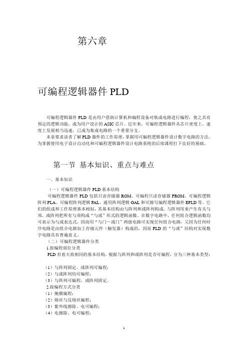
解:1)分析电路结构:该电路是由七个与非门及一个JKFF组成,且CP下降沿触发,属于米勒电路,输入信号X1,X2,输出信号Z。
2)求触发器激励函数:J=X1X2,K =X 1X2触发器次态方程:Q n+1=X1X 2Q n +X 1X2Q n=X1X 2Q n+(X1+X2)Q n电路输出方程:Z = X 1X2Q n+X 1X 2Q n +X1X 2Q n+X1X2Q n3)状态转移表:表6.3.1输入X1X2S(t)Q nN(t)Q n+1输出Z0 0 0 0 0 10 11 0 1 0 1 1 1 101111111111114)X1X2Q n为低位来的进位,Q n+1表示向高位的进位。
且电路每来一个CP,实现一次加法运算,Z为本位和,Q 在本时钟周期表示向高位的进位,在下一个时钟周期表示从低位来的进位。
例如X1=110110,X2=110100,则运算如下表所示:LSB MSB表6.3.2节拍脉冲CP CP1 CP2 CP3 CP4 CP5 CP6 CP7被加数X10 1 1 0 1 1 0加数X20 0 1 0 1 1 0低位进位Q n0 0 0 1 0 1 16.2 试作出101序列检测器的状态图,该同步电路由一根输入线X,一根输出线Z,对应与输入序列的101的最后一个“1”,输出Z=1。
其余情况下输出为“0”。
(1)101序列可以重叠,例如:X:010101101 Z:000101001(2)101序列不可以重叠,如:X:010******* Z:0001000010解:1)S0:起始状态,或收到101序列后重新检测。
S1:收到序列“1”。
S2:连续收到序列“10”。
0/01/0X/Z0/011…100…S2S1S1/00/01/12)0/01/0X/Z0/011…100…S2S1S1/00/01/1解:(1)列隐含表:A B CDCB×A B CDCB×ADBC××(a)(b)进行关联比较得到所有的等价类为:AD,BC。

课程名称英文翻译自然辩证法natural dialectics英语english language数理统计numeral statistic/numerical statistic人工智能及其体系结构artificial intelligence & its architecture高级数理逻辑advanced numerical logic高级程序设计语言的设计与实现advanced programming language s de sign & implementation软件工程基础foundation of software engineering专业英语specialized english计算机网络computer network高级计算机体系结构advanced computer architectureibm汇编及高级语言的接口ibm assembly & its interfaces with advanc ed programming languages分布式计算机系统distributed computer system / distributed system计算机网络实验computer network experiment高等代数elementary algebra数学分析mathematical analysis中共党史history of the chinese communist party算法语言algorithmic language体育physical education英语english language力学实验mechanics-practical德育moral educationpascal语言pascal language政治经济学political economics电学实验electrical experiment数字逻辑mathematical logic普通物理general physics计算方法computing method离散数学discrete mathematics汇编原理principles of assembly概率与统计probability & statistics数据结构data structure哲学philosophy微机原理principles of microcomputer编译方法compilation method系统结构system structure操作系统原理principles of operating system 文献检索documentation retrieval数据库概论introduction to database网络原理principles of network人工智能artificial intelligence算法分析algorithm analysis毕业论文graduation thesisadvanced computational fluid dynamics 高等计算流体力学advanced mathematics 高等数学advanced numerical analysis 高等数值分析algorithmic language 算法语言analogical electronics 模拟电子电路artificial intelligence programming 人工智能程序设计audit 审计学automatic control system 自动控制系统automatic control theory 自动控制理论auto-measurement technique 自动检测技术basis of software technique 软件技术基础calculus 微积分catalysis principles 催化原理chemical engineering document retrieval 化工文献检索circuitry 电子线路college english 大学英语college english test (band 4) cet-4college english test (band 6) cet-6college physics 大学物理communication fundamentals 通信原理comparative economics 比较经济学complex analysis 复变函数论computational method 计算方法computer graphics 图形学原理computer organization 计算机组成原理computer architecture 计算机系统结构computer interface technology 计算机接口技术contract law 合同法cost accounting 成本会计circuit measurement technology 电路测试技术database principles 数据库原理design & analysis system 系统分析与设计developmental economics 发展经济学discrete mathematics 离散数学digital electronics 数字电子电路digital image processing 数字图像处理digital signal processing 数字信号处理econometrics 经济计量学economical efficiency analysis for chemical technology 化工技术经济分析economy of capitalism 资本主义经济electromagnetic fields & magnetic waves 电磁场与电磁波electrical engineering practice 电工实习enterprise accounting 企业会计学equations of mathematical physics 数理方程experiment of college physics 物理实验experiment of microcomputer 微机实验experiment in electronic circuitry 电子线路实验fiber optical communication system 光纤通讯系统finance 财政学financial accounting 财务会计fine arts 美术functions of a complex variable 单复变函数functions of complex variables 复变函数functions of complex variables & integral transformations 复变函数与积分变换fundamentals of law 法律基础fuzzy mathematics 模糊数学general physics 普通物理graduation project(thesis) 毕业设计(论文)graph theory 图论heat transfer theory 传热学history of chinese revolution 中国革命史industrial economics 工业经济学information searches 情报检索integral transformation 积分变换intelligent robot(s); intelligence robot 智能机器人international business administration 国际企业管理international clearance 国际结算international finance 国际金融international relation 国际关系international trade 国际贸易introduction to chinese tradition 中国传统文化introduction to modern science & technology 当代科技概论introduction to reliability technology 可靠性技术导论java language programming java 程序设计lab of general physics 普通物理实验linear algebra 线性代数management accounting 管理会计学management information system 管理信息系统mechanic design 机械设计mechanical graphing 机械制图merchandise advertisement 商品广告学metalworking practice 金工实习microcomputer control technology 微机控制技术microeconomics & macroeconomics 西方经济学microwave technique 微波技术military theory 军事理论modern communication system 现代通信系统modern enterprise system 现代企业制度monetary banking 货币银行学motor elements and power supply 电机电器与供电moving communication 移动通讯music 音乐network technology 网络技术numeric calculation 数值计算oil application and addition agent 油品应用及添加剂operation & control of national economy 国民经济运行与调控operational research 运筹学optimum control 最优控制petroleum chemistry 石油化学petroleum engineering technique 石油化工工艺学philosophy 哲学physical education 体育political economics 政治经济学principle of compiling 编译原理primary circuit (反应堆)一回路principle of communication 通讯原理principle of marxism 马克思主义原理principle of mechanics 机械原理principle of microcomputer 微机原理principle of sensing device 传感器原理principle of single chip computer 单片机原理principles of management 管理学原理probability theory & stochastic process 概率论与随机过程procedure control 过程控制programming with pascal language pascal语言编程programming with c language c语言编程property evaluation 工业资产评估public relation 公共关系学pulse & numerical circuitry 脉冲与数字电路refinery heat transfer equipment 炼厂传热设备satellite communications 卫星通信semiconductor converting technology 半导体变流技术set theory 集合论signal & linear system 信号与线性系统social research 社会调查software engineering 软件工程spc exchange fundamentals 程控交换原理specialty english 专业英语statistics 统计学stock investment 证券投资学strategic management for industrial enterprises 工业企业战略管理technological economics 技术经济学television operation 电视原理theory of circuitry 电路理论turbulent flow simulation and application 湍流模拟及其应用visual c++ programming visual c++程序设计windows nt operating system principles windows nt操作系统原理word processing 数据处理上文已完。


数字电路面试题Digital Circuit Interview QuestionsIntroduction:In today's technological era, digital circuits serve as the cornerstone of various electronic devices and systems. It is essential for individuals involved in the field of electrical engineering to possess a comprehensive understanding of digital circuits. This article presents a selection of frequently asked interview questions regarding digital circuits, providing insights into key concepts, design methodologies, and problem-solving abilities.Question 1: What is a digital circuit?A digital circuit is a network of interconnected electronic components designed to process digital signals or information in the form of "bits" - binary digits. These circuits utilize logic gates, flip-flops, registers, and other building blocks to perform operations such as arithmetic, logic, and memory functions.Question 2: Differentiate between combinational and sequential logic circuits.Combinational logic circuits generate an output based solely on the current input values. They lack memory elements, ensuring that the output is solely determined by the present inputs. Conversely, sequential logic circuits output not only depend on the present inputs but also on the past inputs and stored information, using memory elements such as flip-flops.Question 3: How can you convert a given logic circuit into its corresponding truth table?To convert a logic circuit into a truth table, one needs to consider all possible input combinations. For each combination, determine the output based on the circuit's logic gates and connections. The resulting truth table will list all possible input combinations alongside their corresponding output values.Question 4: Explain the concept of propagation delay in digital circuits.Propagation delay refers to the time taken for the output of a logic gate to change in response to a change in its input. It is caused by the finite speed of signal transmission within digital circuits due to factors such as gate delays and interconnect lengths. Minimizing propagation delays is crucial to ensure proper circuit operation and timing.Question 5: What is Moore's law, and how does it relate to digital circuits?Moore's law, formulated by Gordon Moore, states that the number of transistors in an integrated circuit doubles approximately every two years. This observation highlights the trend of exponentially increasing computational power and efficiency in digital circuits over time. Integrated circuits incorporating more transistors enable the design and implementation of complex digital systems.Question 6: Describe the concept of clock skew in clock distribution networks.Clock skew refers to the variation in arrival times of clock signals across different components or clock distribution lines within a digital circuit. It can lead to synchronization issues and affect the proper functioning of sequential logic circuits. Minimizing clock skew is crucial to maintain accurate timing and prevent data corruption.Question 7: What are the commonly used design methodologies for digital circuits?Several design methodologies are employed in digital circuit design, including the following:1. RTL (Register Transfer Level) Design: Describing the circuit's behavior using high-level abstractions, focusing on the flow of data between registers.2. Gate-Level Design: Utilizing predefined standard cells and logic gates to implement the circuit's functionality.3. Behavioral Design: Describing the circuit's behavior using programming languages such as VHDL or Verilog to simulate and synthesize the design.4. Physical Design: Involves designing the layout and placement of components, considering factors such as power consumption, noise, and heat dissipation.Question 8: Discuss the concept of hazard in digital circuits.In digital circuits, a hazard refers to a temporary glitch or deviation in the expected output caused by a transition in the input signals. Hazards canoccur due to circuit delays, complex combinational paths, or improper synchronization. Designers must identify and eliminate hazards through techniques such as hazard coverings or hazard-free logic restructuring.Question 9: Explain the advantages and disadvantages of using FPGA (Field-Programmable Gate Array) in digital circuit design.Advantages:1. Versatility: FPGA allows rapid prototyping and design alterations, eliminating the need for fabricating custom integrated circuits.2. Flexibility: Designs can be modified or reprogrammed as required, providing flexibility in adapting to changing requirements.3. Time-to-Market: FPGA-based designs can be developed and deployed quickly, reducing the time required to bring a product or solution to market.4. Cost-Efficiency: FPGA eliminates the high upfront costs associated with ASIC (Application-Specific Integrated Circuit) production.Disadvantages:1. Power Consumption: FPGA can consume more power compared to ASIC, impacting battery-powered devices.2. Limited Scalability: FPGA designs may face limitations in terms of size, complexity, and performance compared to ASIC designs.3. Higher Unit Cost: While FPGA offers cost benefits for low to medium volume production, it may become costlier for high-volume production due to per-unit costs.Question 10: How do you mitigate hazards caused by glitches in digital circuits?To mitigate hazards caused by glitches, designers can employ the following techniques:1. Use Gate Delay Elements: Introduce specialized elements within the circuit to ensure uniform delays and minimize glitches.2. Hazard Covering: Introduce additional logic elements to detect and fix hazards.3. Logic Restructuring: Optimize the circuit's logic gates and structural elements to eliminate or reduce potential hazards.4. Pipeline the Circuit: Introduce pipeline stages to divide the circuit into smaller sections, ensuring proper synchronization and reducing hazards.Conclusion:Digital circuit knowledge and problem-solving skills are crucial for individuals seeking a career in electrical engineering or related fields. By understanding the fundamental concepts, design methodologies, and problem-solving approaches, one can confidently tackle digital circuit interview questions, paving the way for success in this domain. Remember to stay updated with the latest advancements and continuously enhance your skills as digital circuit technology continues to evolve.。


附录1 译文数字电路介绍数字电路定义:用数字信号完成对数字量进行算术运算和逻辑运算的电路称为数字电路,或数字系统。
由于它具有逻辑运算和逻辑处理功能,所以又称数字逻辑电路。
数字逻辑电路分类(按功能分):1、组合逻辑电路简称组合电路,它由最基本的的逻辑门电路组合而成。
特点是:输出值只与当时的输入值有关,即输出惟一地由当时的输入值决定。
电路没有记忆功能,输出状态随着输入状态的变化而变化,类似于电阻性电路,如加法器、译码器、编码器、数据选择器等都属于此类。
2、时序逻辑电路简称时序电路,它是由最基本的逻辑门电路加上反馈逻辑回路(输出到输入)或器件组合而成的电路,与组合电路最本质的区别在于时序电路具有记忆功能。
时序电路的特点是:输出不仅取决于当时的输入值,而且还与电路过去的状态有关。
它类似于含储能元件的电感或电容的电路,如触发器、锁存器、计数器、移位寄存器、储存器等电路都是时序电路的典型器件。
数字电路的特点:1、同时具有算术运算和逻辑运算功能数字电路是以二进制逻辑代数为数学基础,使用二进制数字信号,既能进行算术运算又能方便地进行逻辑运算(与、或、非、判断、比较、处理等),因此极其适合于运算、比较、存储、传输、控制、决策等应用。
2、实现简单,系统可靠以二进制作为基础的数字逻辑电路,简单可靠,准确性高。
3、集成度高,功能实现容易集成度高,体积小,功耗低是数字电路突出的优点之一。
电路的设计、维修、维护灵活方便,随着集成电路技术的高速发展,数字逻辑电路的集成度越来越高,集成电路块的功能随着小规模集成电路(SSI)、中规模集成电路(MSI)、大规模集成电路(LSI)、超大规模集成电路(VLSI)的发展也从元件级、器件级、部件级、板卡级上升到系统级。
电路的设计组成只需采用一些标准的集成电路块单元连接而成。
对于非标准的特殊电路还可以使用可编程序逻辑阵列电路,通过编程的方法实现任意的逻辑功能。
数字电路的应用:数字电路与数字电子技术广泛的应用于电视、雷达、通信、电子计算机、自动控制、航天等科学技术各个领域。


4§6.2 Synchronic Sequential Circuit Analysis同步时序电路分析Example 1: Analysis the sequential circuit 分析下面时序电路Analysis: Given a circuit, describe its operation.1)Inputs OutputsControl inputs StatesX ZJ 0, K 0, J 1, K 1Q 1 (MSB), Q 01()n n Z X Q Q=⊕⋅01n J X Q=⊕10nJ X Q =⊕1K =Driving equationOutput equation 2) Equations状态图的主循环:模3加减双向计数器X=0, 模3加法计数器:Z=1,进位输出;12§6.3 Synchronous Sequential Circuit Design时序逻辑电路设计3) State distribution (状态分配或状态编码encoding)Known →State diagram 状态图Request →Circuit 电路1) Determine state and state diagram 确定状态、状态图2) State simplification 状态化简5) Q n+1equations and control inputs –J, K, D, T 驱动方程Design steps:6) Circuit 电路4) Select FF 选择触发器7)Self start (检查能否自启动)/1/1 /1205) 列驱动方程D 1 = XQ 0n D 0 = XY= XQ 1n2 D-FFs 6) 画电路图1/0010/01/0110/01/10001§6.4 Counter 计数器计数器是用于统计输入脉冲CLK个数的电路。

第六章 习题解答6.1. 分析题图P6.1所示电路的功能,列出功能表。
解:图P6.1所示电路的功能表如表6.1所示。
将功能表中各变量数值关系的逻辑函数用对应的“卡诺图”如图6.1所示。
RS 具有约束条件RS =0,触发器的逻辑表达式为⎪⎩⎪⎨⎧=+=+0RS Q R S Q n 1n ,根据这一逻辑表达式,P6.1逻辑电路具有基本RS 触发器的逻辑功能,约束条件是SR=0。
6.2同步RS 触发器与基本RS 触发器的主要区别是什么?解:同步RS 触发器与基本RS 触发器的主要区别是基本RS 触发器的RS 输入信号不论任何时刻都是有效的,只要RS 输入的状态组合发生变化,输出Q 的状态跟随发生变化;而同步同步RS 触发器的RS 输入信号只要在CP 时钟脉冲信号有效时段内起作用,只有在这一时段内,输出Q 的状态才跟随RS 输入的状态组合变化而发生变化。
1& & 1QR图 P6.1QR S Q nQ n+1功 能 1 1 1 1 0 1 不用 不用 不允许11 0 0 0 1 0 0 01=+n Q 置0 0 0 1 1 0 1 1 1 11=+n Q 置10 00 00 10 1n n Q Q =+1 保持6.3如图P6.3 (a)所示电路的初始状态为Q =1,R 、S 端和CP 端的信号如图P6.3(b )所示,画出该同步RS 触发器相应的Q 和Q 端的波形。
解:根据图P6.3 (a)所示电路结构,其功能为同步RS 触发器,电路的特性方程为:⎪⎩⎪⎨⎧=+=+0RS Q R S Q n 1n ,若R=S=1,在CP 时钟脉冲信号为“1”的时段内,触发器的两个输出端的状态均输出“1”,此种情况下,若CP 时钟脉冲信号从“1”状态,跳变为“0”的输入状态,则触发器的两个输出状态为不确定状态。
根据特性方程以及电路的初始状态,作出电路的输出端时序图如图6.3所示。
6.4 主从RS 触发器输入信号的波形如图P6.4(a )、(b )所示。

时序逻辑电路的基本概念
1. 时序电路的一般化模型
O
电路由组合电路和存储电路组成。
电路存在反馈。
输出方程: O=f1(I,S)
表达输出信号与输入信号、状态变量的关系式
激励方程: E=f2(I,S)
表达了激励信号与输入信号、状态变量的关系式
状态方程: S n+1=f3(E,S n)
表达存储电路从现态到次态的转换关系式
2、异步时序电路与同步时序电路
存储电路里所有触发器有一个统一的时钟源,它们的状态在同一时刻更新。
没有统一的时钟脉冲或没有时钟脉冲,电路的状态更新不是同时发生的。
2.时序逻辑电路的分析
分析时序逻辑电路在输入信号的作用下,其状态和输出信号变化的规律,进而确定电路的逻辑功能。
时序电路的逻辑能是由其状态和输出信号的变化的规律呈现出来的。
所以,分析过程主要是列出电路状态表或画出状态图、工作波形图。
1.了解电路的组成:
电路的输入、输出信号、触发器的类型等
2. 根据给定的时序电路图,写出下列各逻辑方程式:
(1) 输出方程;
(2) 各触发器的激励方程;
(3)状态方程: 将每个触发器的驱动方程代入其特性方程得状态方程.
3.列出状态转换表或画出状态图和波形图;
4.确定电路的逻辑功能.。


M o d u l e 6: C o m b i n a t i o n a l C i r c u i t B l o c k sRevision: August 31, 2009215 E Main Suite D | Pullman, WA 99163(509) 334 6306 Voice and FaxContains material © Digilent, Inc. 11 pagesOverviewThis lab introduces several combinational circuits that are frequently used by digital designers,including a data selector (also called a multiplexor or just "mux"), a binary decoder, a seven-segment decoder, an encoder, and a shifter. Each of these circuits can be used by themselves in the solution of some simpler logic problems, but they are more often used as building blocks in the creation of larger, more complex circuits. In this module, these circuits will be developed from first principles following a general design procedure that will serve as a model for all later designs. In later modules, these circuits will be used as modular (or “macro”) building blocks in larger designs.This general design procedure has five main steps. First, you must gain a clear understanding of the design intent of each circuit before any design activities start. When you are doing original design work, this understanding comes from many sources, including other persons, previous or competing designs, research papers, or your own insightful thinking. For now, the discussion that leads thepresentation of each new circuit is intended to impart that clear understanding to you. Second, a block diagram that shows all circuit inputs and outputs will be developed. A block diagram is anindispensable part of any design, especially when dealing with complex circuits. In conceiving and capturing a block diagram, you are committing to a set of input and output signals, and those signals define the context and boundaries of your design. Third, the design requirements will be captured in an engineering formalism like a truth table or logic equations. This formalism removes all ambiguity from the design, and establishes a solid specification for the circuit. Fourth, the formally stated requirements will be used to find minimal circuits that meet the specifications. And finally, those minimal circuits will be created and implemented using the ISE/WebPack tool and a Digilent board, and verified in hardware to ensure they meet their behavioral requirements.Before beginning this lab, you should… After completing this lab, you should…• Be able to specify, design, and minimize combinational logic systems• Be able to create schematic-based orVHDL-based designs in the Xilinx WebPack environment• Be able to download designs created inWebPack to the Digilent circuit board.• Understand the application, function, andstructure of decoder, multiplexor, encoder, and shifter circuits; • Know how to use these circuits in thesolution of larger problems; • Be able to quickly implement these circuits in the Xilinx CAD tool environment.This lab exercise requires…• A windows computer running Xilinx WebPack • A Digilent boardCombinational Circuit BlocksData Selectors (Multiplexors)Data selectors, more commonly called multiplexors (or just muxes), function by connecting one of their input signals to their output signal as directed by their “select” or control input signals. Muxes have N data inputs and log2N select inputs, and a single output. In operation, the select inputs determine which data input drives the output, and whatever voltage appears on the selected input is driven on the output. All non-selected data inputs are ignored. As an example, if the select inputs of a 4:1 mux are ‘1’ and ‘0’, then the output Y will be driven to the same voltage present on input I2.Common mux sizes are 2:1 (1 select input), 4:1 (2 select inputs), and 8:1 (3 select inputs). The truth table shown specifies the behavior of a 4:1 mux. Note the use of entered variables in the truth table – if entered variables were notused, the truth table would require six columns and 26 or 64 rows. In general, when entered-variable truth tables are used to define a circuit, “control” inputs are shown as column-heading variables, and data inputs are used an enteredvariables.The truth table can easily be modified for muxes that handle different numbers of inputs, by adding or removing control input columns. A minimal mux circuit can be designed by transferring the information in the truth table to a K-map, or by simply inspecting the truth table and writing an SOP equation directly. A minimal equation for the 4:1 mux follows (you are encouraged to verify this is a minimal equation):computer circuits must switch 8, 16, 32 or more signals all at once. Muxes that can switch many signals simultaneously are called “bus muxes”. A block diagram and schematic for a bus mux that can select one of four 8-bit data elements is shown below.A[7:0] B[7:0] C[7:0] D[7:0]Y[7:0]Y[7:0] A[7:0]B[7:0]C[7:0]D[7:0]S0S1S1S0Since this most common application of multiplexors is beyond our current presentation, we will consider a less common, somewhat contrived application. Consider the K-map representation of a given logic function, where each K-map cell contains a '0', '1', or an entered variable expression. Each unique combination of K-map index variables selects a particular K-map cell (e.g., cell 6 of an 8 cell K-map is selected when A=1, B=1, C=0). Now consider a mux, where each unique combination of select inputs selects a particular data input to be passed to the output (e.g., I6 of an 8 input mux can be selected by setting the select inputs to A=1, B=1, C=0). It follows that if the input signals in a given logic function are connected to the select inputs of a mux, and those same input signals are used as K-map index variables, then each cell in the K-map corresponds to a particular mux data input. This suggests a mux can be used to implement a logic function by “connecting” the K-map cell contents to the data lines of the mux, and connecting the K-map index variables to the select lines of the mux. Mux data inputs are connected to: '0' (or ground) when the corresponding K-map cell contains a '0'; '1' (or Vdd) when the corresponding K-map cell contains a '1'; and if a K-map cell contains an entered variable expression, then a circuit implementing that expression is connected to the corresponding mux data input. Note that when a mux is used to implement a logic circuit directly from a truth table or K-map, logic minimization is not performed. This saves design time, but usually creates a less efficient circuit (however, a logic synthesizer would remove the inefficiencies before such a circuit was implemented in a programmable device).A mux can easily be described in behavioral VHDL using a selected signal assignment statement as shown below. The statement functions by comparing the value of the sel input to the value shown in the when clause: the output variable Y gets assigned I0, I1, I2, or I3 depending on whether sel = “00”, “01”, “10”, or “11” (in a selected signal assignment statement, the “when others” clause is used for the final case for reasons that will be explained later). In addition to assigning values to individual signals or busses, the selected signal assignment statement can also be used to assign the result of arithmetic and/or logic operations to an output.The example code on the left below is for a mux that switches logic signals, and the code on the right is for an 8-bit bus mux. Note the only difference in the code is in the port statement, where the data elements for the bus mux are declared to be vectors instead of signals. Note also that the assignment statement in the bus mux example assigns vector quantities just like signals. When you examine the code examples, particularly the bus mux, look again at the previous figure and consider the amount of effort required to create a bus mux schematic vs. the bus mux VHDL code.VHDL source code for implementing a morecomplex mux’ing circuit, such as one thatmight select any one of four logic functionoutputs to pass through to the output, isshown on the right. This example code usesa “conditional assignment” statement.Conditional assignment statements andselected signal assignments both allowmore complex logic requirements to besuccinctly described, and they can generallybe used interchangeably. In most cases, asynthesizer will produce the same circuitregardless of whether a selected orconditional assignment statement is used.There are subtle differences between thestatements, and these differences will be discussed later. For now, it is a matter of personal taste as to which one is used.VHDL code for a mux using a conditional assignmentA conditional assignment statement uses the “when-else” language feature to describe compound logic statements. By following the example code shown, conditional assignments can be written to describe a wide variety of assignments.DecodersDecoder circuits receive inputs in the form of an N-bit binary number and generate one or more outputs according to some requirement. Decoder inputs are typically viewed as a binary numberrepresenting some encoded quantity, and outputs typically drive some other circuit or device based on decoding that quantity. For example, a PS/2 keyboard decoder decodes the “scan codes” that are generated each time a given key is pressed (scan codes are unique binary numbers that are assigned to individual keys on a PS/2 keyboard). Most scan codes are simply sent to the host computer forparsing, but some perform specific functions. If the “caps lock” key is pressed, a signal is generated to illuminate an LED on the keyboard, and if “Cntrl-Alt-Del” is pressed, a signal is generated to interrupt PC operations.Here, we will examine two different types of decoders – a simple binary decoder, and a seven-segment decoder that can drive a common numeric data display.A binary decoder has N inputs and 2N outputs. It receives N inputs (often grouped as a binary number on a bus) and then asserts one and only one of its 2N outputs based on that input. If the N inputs are taken as an N-bit binary number, then only the output that corresponds to the input binary number is asserted. For example, if a binary 5 (or "101") is input to a 3:8 decoder, then only the 5th output of the decoder will be asserted and all other outputs will be de-asserted. Practicaldecoder circuits are usually built as 2:4 decoders with 2 inputs and 22 (4) outputs, 3:8 decoders with 3 inputs and 23 (8) outputs, or 4:16 decoders with 4 inputs 24 (16) outputs. A decoder circuit requires one AND gate to drive each output, and each AND gate decodes a particular binary number. For example, a 3:8 decoderrequires 8 AND gates, with the first AND gate having inputs A’· B’· C’, the secondA’· B’· C, the third A’· B · C’, etc.If a binary decoder larger than 4:16 is needed, it can be built from smaller decoders. Only decoders with an enable input can be used to construct larger decoder circuits. As with the mux, the enable input drives all outputs to ‘0’ when de-asserted, and allows normal decoder operation when asserted.Decoders are most often used in more complex digital systems to access a particular memory location based on an “address” produced by a computing device. In this application, the addressrepresents the coded data inputs, and the outputs are the particular memory element select signals. A typical memory circuit contains a decoder to select which memory element to write, the memory elements themselves, and a mux to select which element to read.As with multiplexors, this most common application of decoders is beyond our current presentation, so instead we will consider a less common, somewhat contrived application. Consider the function of a decoder and the truth table, K-map, or minterm representation of a given function. Each row in a truth table, each cell in a K-map, or each minterm number in an equation represents a particularcombination of inputs. Each output of a decoder is uniquely asserted for a particular combination of inputs. Thus, if the inputs to a given logic function are connected to the inputs of a decoder, and those same inputs are used as K-map input logic variables, then a direct one-to-one mapping is created between the K-map cells and the decoder outputs. It follows that any given function represented in a3:8 binary decodertruth table or K-map can be directly implemented using a decoder, by simply by OR'ing the decoder outputs that correspond to a truth table row or K-map cell containing a “1” (decoder outputs thatcorrespond to K-map cells that contain a zero are simply left unconnected). In such a circuit, any input combination with a ‘1’ in the corresponding truth table row or K-map cell will drive the output OR gate to a ‘1’, and any input combination with a ‘0’ in the corresponding K-map cell will allow the OR gate to output a ‘0’. Note that when a decoder is used to implement a circuit directly from a truth table or K-map, no logic minimization is performed. Using a decoder in this fashion saves time, but usually results in a less efficient implementation (here again, a logic synthesizer would remove theA decoder can easily be described inbehavioral VHDL using a selected signalassignment statement as shown below. Inthe example, both the inputs and outputs are grouped as busses so that a selected assignment statement can be used. In this example, the inputs can be individually referred to as I(1) and I(0), and the outputs as Y(0) through Y(3). The code can easily be modified to describe a decoder of any size. De-multilpexorOur use of the word “multiplexor” has its origins in telecommunications, defining a system where one signal is used to transmit many different messages, either simultaneously or at different times. “Time-multiplexing” describes a system where different messages use the same physical signal, withdifferent messages being sent at different times. Time multiplexing works if a given signal can carry more traffic than any one message needs. For example, if ten messages each require that 1Kbit of information be sent every second, and if a communication signal is available that can carry 10Kbits per second, then time-multiplexing can be used to provide ten 1Kbit time windows each second, one for each signal. A multiplexor can be used as a simple time multiplexor, if the select inputs are used to define the time window, and the data inputs are used as the data sources.A decoder with an enable can be usedas a de-multiplexor. Whereas a multiplexor selects one on N inputs to pass through to the output, a de-multiplexor takes a single input and routes it to one of N outputs. A multiplexor/de-multiplexor (or more simply, mux/de-mux) circuit can be used to transmit the state of N signals from one place to another using only Log 2N+1 signals. Log 2N signals areused to select the data input for the mux and to drive the decoder inputs, and the rate at which these signals change define the time-window length. The data-out of the mux drives the enable-in of the decoder, so that the same logic levels that appear on the mux inputs also appear on thecorresponding decoder outputs, but only for the mux input/decoder output currently selected. In thisway, the state of N signals can be sent from one place to another using only Log 2N+1 signals, but only one signal at a time is valid.Seven-Segment Displays and DecodersSeven-segment displays (7sd) are some of the most common electronic display devices in use. They can be used to display any decimal digit by illuminating particular segments and leaving othersegments dark. 7sd devices are constructed from seven LEDs that have been arranged in a figure "8" pattern as shown in the figure below. These LEDs function identically to the individual LEDs – they emit light when a small current passes through them. The 7sd device can display a particular digit if certain LED segments are illuminated while others remain dark. As examples, if only segments b and c are illuminated, then the display will show a '1', and if segments a, b and c are illuminated then the display will show a '7'. To cause an illuminating current to flow through any given LED segment, a logic signal must be impressed across thesegment LED. In a typical 7sd circuit, a current-limiting resistor is placed on the cathode lead, and a transistor is used on the anode lead toprovide additional current (most signal pins ondigital ICs – like the FPGA on the Digilent board – cannot provide enough current to light all the display segments, so a transistor is used to provide more current). In order that all 10 decimal digits can be displayed, a 7sd device requires seven logicsignals, one for each segment. By assertingparticular combinations of these signals, all tendecimal digits can be displayed.The Digilent board uses a common anode display, which means that all the anode connections for asegment in a given digit, a ‘1’ must be applied to the digit’s anode, and ‘0’ must be applied to the segment’s cathodes (NOTE: With Digilent boards, a ‘1’ is applied to a digit’s anode by applying a ‘0’ to the circuit node that drives the transistor; thus, the anode signals AN3 – AN0 are “active low”).A seven-segment decoder (SSD) receives four signals that represent the four bits of a binary number, and produces seven output signals that can drive the seven segments in the seven-segment display. Thus, for example, if “0000” is input to the SSD, all outputs except “g” should be asserted (to cause a ‘0’ to bedisplayed on the 7sd). And if “1000” is input to the SSD, then all outputs should be asserted (to cause an ‘8’ to be displayed). Typically, the input signals are named B3-B0, and the output signals are given a letter to indicate which segment they must drive (A-F). As discussed above, each of the seven outputs could be thought of as a separate 4-input logic design C B3B(3:0)problem, and optimal circuits for each output could easily be found using the techniques developed in previous labs. In lab project that accompanies this module, various methods will be used to optimize (or minimize) the system as a whole, considering all seven outputs at the same time.A 7sd can easily be described in VHDL using a selected signal assignment statement. In fact, a selected assignment statement can be used to implement any truth table by listing the function inputs on the right of the” when” clause, and the associated outputs on the left. In the example shown below, the input and output variables are both vectors – the ins represents a 2-bit binary number, and the outs represent a 4-bit binary number. As discussed in the “muxes” section above, the output variable outs gets assigned the binary values shown in quotes when ins is equal to the value in the “when” clause. Thus, if ins is "01", then outs gets assigned "1010".VHDL code for a seven-segment decoder is partially supplied below. The four inputs (representing a binary number) have been grouped into a vector called BIN, and the seven segment outputs have been grouped into a vector called SEG_OUT. Note the "when others" clause in the last line as is typical for any selected assignment statement. This catch-all “when others” clause is used to assign the value "0000001" to the seven segment decoder outputs whenever an unspecified input condition occurs. In this case, this clause can be used to assign an output value when the binary numbers 1010 through 1111 are present on the inputs.Example VHDL code for a Seven-Segment DecoderPriority EncodersA priority encoder is, in a sense, the dual (or opposite) of the decoder circuit – itreceives N inputs (where N is typically 4, 8 or 16), and asserts an output binarycode of M=log2N bits (so the M-bit binary code is typically 2, 3, or 4 bits). The M-bitbinary code indicates which input was asserted (i.e., in a 4:2 binary encoder, binarycode 00 would be output if the 0th input line was asserted, binary code 01 would beoutput of the 1st input line was asserted, etc.). Since more than one input line to theencoder might be asserted at any given time, the priority encoder asserts an outputcode corresponding to the highest numbered input that is asserted (i.e., if both input line 0 and input line 2 were asserted in a 4:2 encoder, then binary code 10 would be output indicating that input line 2 is the highest line number – or highest priority input – currently asserted).At first thought, a four input encoder circuit should require just two outputs. In such a circuit, asserting the 3rd input signal would cause a “11” output, asserting the 2nd input signal would output a “10”, asserting the 1st input signal would output a “01”, and asserting the 0th input would output “00”. But what if no inputs are asserted? Again, a “00” would be appropriate. To avoid creating an ambiguous “00” output, encoders typically use an “Enable In” (E IN) signal and an “Enable Output” (E OUT) signal.E IN functions like other enable signals – when it is de-asserted, all outputs are driven to logic ‘0’, and when it is asserted, the encoder outputs can be driven by the inputs. E OUT is asserted only when E IN is asserted and no input signals are asserted. Thus, E OUT can be used to distinguish between no inputs asserted and the 0th input asserted.Larger encoders can be built from smaller encoder modules in much the same way that larger decoders can be built from smaller decoder modules. An encoder module that can be used as a building block for larger encoders must have one additional output called group-signal (GS). GS is asserted whenever E IN is asserted along with any other input signal, and it is used to form the most significant bit of the encoded output data element.Encoder circuits are typically used in digital systems when a binary number that corresponds to a given input must be generated. For example, individual “call attendant” signals arising from passengers seated on an airplane could be encoded into a seat number. Priority encoders are also used when certain input signals must be dealt with in a special manner. For example, if inputs from several sources can all arrive simultaneously, a priority encoder can indicate which signal should be dealt with first. Behavioral VHDL code for an encoder is shown below.ShiftersA shifter is a circuit that produces an N-bit output based on an N-bit data input and an M-bit control input, where the N output bits are place-shifted copies of the input bits, shifted some number of bits to the left or right as determined by the control inputs. As an example, the function of an 8-bit shifter capable of shifting one, two, or three bits to the right or left is illustrated in the top row of the figure below. The control signals enable several different functions: two bits (A 1 and A 0) to determine how many bit positions to shift (0, 1, 2, or 3); a Fill signal (F) determines whether bits vacated by shiftoperations receive a ‘1’ or a ‘0’; a Rotate signal (R = ‘1’ for rotate) determines whether shifted-out bits are discarded or recaptured in vacated bits; and a Direction signal (D = ‘1’ for right) determines which direction the shift will take.Module #6: Combinational Circuit BlocksShifters are most often found in circuits that work with groups of signals that together represent binary numbers, where they are used to move data bits to new locations on a data bus (i.e., the data bit in position 2 could be moved to position 7 by right shifting five times), or to perform simple multiplication and division operations (exactly why a bit might want to be moved from one location to another on a data bus is left for a later module). A shifter circuit can multiply a number by 2, 4, or 8 simply by shifting the number right by 1, 2, or 3 bits (and similarly, a shifter can divide a number by 2, 4, or 8 by shifting the number left by 1, 2, or 3 bits).A behavioral VHDL design of a simple 8-bit shifter that can shift or rotate left or right by one bit is shown below. A conditional assignment statement is used in this example as the only statement in the architecture body. The “when-else” clause evaluates the state of enable (en), rotate (r), and direction (d) to distinguish between the possible output vector signal assignments. The first assignment in the conditional assignment statement assigns all zero’s to the dout bus when en=’0’. The remaining four assignments make use of the concatenation operator (&) to assign shifted or rotated versions of the input data bus to the output bus, depending on the states of r and d.。
