MAX6125ESA中文资料
- 格式:pdf
- 大小:717.99 KB
- 文档页数:9

For pricing, delivery, and ordering information, please contact /Dallas Direct! at1-888-629-4642, or visit Maxim’s website at _______________General Description The MAX1482 and MAX1483 are low-power trans-ceivers for RS-485 and RS-422 communication. Both feature slew-rate-limited drivers that minimize EMI and reduce reflections caused by improperly terminated cables. Data rates are guaranteed up to 250kbps.The MAX1482/MAX1483 draw only 20µA of supply cur-rent. Additionally, they have a low-current shutdown mode that consumes only 0.1µA. Both parts operatefrom a single +5V supply.Drivers are short-circuit current limited and are protect-ed against excessive power dissipation by thermal shutdown circuitry that places the driver outputs into a high-impedance state. The receiver input has a fail-safefeature that guarantees a logic-high output if the input is open circuit.The MAX1482 is full duplex and the MAX1483 is half duplex. Both parts have a 1⁄8-unit-load input impedancethat guarantees up to 256 transceivers on the bus.________________________Applications Low-Power RS-485/RS-422 Networks Transceivers for EMI-Sensitive Applications Industrial-Control Local Area Networks Large 256-Node LANs ____________________________Features ♦Low 20µA Operating Current♦Slew-Rate Limited for Reduced EMI and Reduced Reflections♦0.1µA Low-Current Shutdown Mode♦Designed for RS-485 and RS-422 Applications ♦Operate from a Single +5V Supply♦-7V to +12V Common-Mode Input Voltage Range ♦Allows up to 256 Transceivers on the Bus—Guaranteed (1⁄8-unit load)♦Current Limiting and Thermal Shutdown for Driver Overload ProtectionMAX1482/MAX1483________________________________________________________________ Integrated Products 1_________________Pin Configurations_________Typical Operating Circuits Ordering Information µMAX is a registered trademark of Integrated products, Inc.找MEMORY 、二三极管上美光存储M A X 1482/M A X 1483Line Length vs. Data Rate The RS-485/RS-422 standard covers line lengths up to 4000 feet. For line lengths greater than 4000 feet, see Figure 16.Figure 13 shows the system differential voltage for the parts driving 4000 feet of 26AWG twisted-pair wire at 110kHz into 120Ωloads. Even after 4000 feet of cable,the MAX1482/MAX1483 output shows virtually no dis-tortion.Typical Applications The MAX1482/MAX1483 transceivers are designed forbidirectional data communications on multipoint bus transmission lines. Figures 14 and 15 show typical net-work applications circuits. These parts can also be used as line repeaters, with cable lengths longer than 4000 feet, as shown in Figure 16.To minimize reflections, the line should be terminated at both ends in its characteristic impedance, and stub lengths off the main line should be kept as short as possible (although the slew-rate-limited MAX1482 and MAX1483 are more tolerant of imperfect termination than standard RS-485 ICs).Isolated RS-485For isolated RS-485 applications, see the MAX253 and MAX1480 data sheets.20µA, 1⁄8-Unit-Load, Slew-Rate-Limited RS-485 Transceivers 10______________________________________________________________________________________Figure 14. MAX1483 Typical Half-Duplex RS-485 NetworkR O DI RECEIVER INPUTV Y -V Z 2µs/div 5010-150Figure 13. System Differential Voltage at 250kbps (125kHz)Driving 4000 Feet of Cable。


2Maxim Integrated Supply Voltage (V CC ) (12V)Control Input Voltage (RE , DE)...................-0.5V to (V CC + 0.5V)Driver Input Voltage (DI).............................-0.5V to (V CC + 0.5V)Driver Output Voltage (A, B)...................................-8V to +12.5VReceiver Input Voltage (A, B).................................-8V to +12.5VReceiver Output Voltage (RO)....................-0.5V to (V CC + 0.5V)Continuous Power Dissipation (T A = +70°C)8-Pin Plastic DIP (derate 9.09mW/°C above +70°C)....727mW14-Pin Plastic DIP (derate 10.00mW/°C above +70°C)..800mW8-Pin SO (derate 5.88mW/°C above +70°C).................471mW 14-Pin SO (derate 8.33mW/°C above +70°C)...............667mW 8-Pin µMAX (derate 4.1mW/°C above +70°C)..............830mW 8-Pin CERDIP (derate 8.00mW/°C above +70°C).........640mW 14-Pin CERDIP (derate 9.09mW/°C above +70°C).......727mW Operating Temperature Ranges MAX4_ _C_ _/MAX1487C_ A...............................0°C to +70°C MAX4__E_ _/MAX1487E_ A.............................-40°C to +85°C MAX4__M_/MAX1487MJA.............................-55°C to +125°C Storage Temperature Range.............................-65°C to +160°C Lead Temperature (soldering, 10sec).............................+300°C DC ELECTRICAL CHARACTERISTICS(V CC = 5V ±5%, T A = T MIN to T MAX , unless otherwise noted.) (Notes 1, 2)Stresses beyond those listed under “Absolute Maximum Ratings” may cause permanent damage to the device. These are stress ratings only, and functional operation of the device at these or any other conditions beyond those indicated in the operational sections of the specifications is not implied. Exposure to absolute maximum rating conditions for extended periods may affect device reliability.VV IN = -7V V IN = 12V V IN = -7V V IN = 12V Input Current (A, B)I IN2V TH k Ω48-7V ≤V CM ≤12V, MAX487/MAX1487R INReceiver Input Resistance -7V ≤V CM ≤12V, all devices exceptMAX487/MAX1487R = 27Ω(RS-485), Figure 40.4V ≤V O ≤2.4VR = 50Ω(RS-422)I O = 4mA, V ID = -200mV I O = -4mA, V ID = 200mV V CM = 0V -7V ≤V CM ≤12V DE, DI, REDE, DI, RE MAX487/MAX1487,DE = 0V, V CC = 0V or 5.25VDE, DI, RE R = 27Ωor 50Ω, Figure 4R = 27Ωor 50Ω, Figure 4R = 27Ωor 50Ω, Figure 4DE = 0V;V CC = 0V or 5.25V,all devices exceptMAX487/MAX1487CONDITIONS k Ω12µA ±1I OZR Three-State (high impedance)Output Current at Receiver V 0.4V OL Receiver Output Low Voltage3.5V OH Receiver Output High VoltagemV 70ΔV TH Receiver Input HysteresisV -0.20.2Receiver Differential ThresholdVoltage-0.2mA 0.25mA -0.81.01.55V OD2Differential Driver Output(with load)V 2V 5V OD1Differential Driver Output (no load)µA ±2I IN1Input Current V 0.8V IL Input Low VoltageV 2.0V IH Input High VoltageV 0.2ΔV OD Change in Magnitude of DriverCommon-Mode Output Voltagefor Complementary Output StatesV 0.2ΔV OD Change in Magnitude of DriverDifferential Output Voltage forComplementary Output StatesV 3V OC Driver Common-Mode OutputVoltageUNITS MIN TYP MAX SYMBOL PARAMETER找MEMORY 、二三极管上美光存储Low-Power, Slew-Rate-Limited RS-485/RS-422 Transceivers12Maxim Integrated MAX481/MAX483/MAX485/MAX487–MAX491/MAX1487500mV/div 20ns/div ABRO 2V/divV CC = 5V T A = +25°C 500mV/div 20ns/divAB RO2V/divV CC = 5V T A = +25°C500mV/div 400ns/div ABRO2V/div V CC = 5V T A = +25°C 500mV/div 400ns/divA B RO2V/div V CC = 5VT A = +25°CFigure 14. Receiver Propagation Delay Test CircuitFigure 15. MAX481/MAX485/MAX490/MAX491/MAX1487Receiver t PHL Figure 16. MAX481/MAX485/MAX490/MAX491/MAX1487Receiver t PLHPHL Figure 18. MAX483, MAX487–MAX489 Receiver t PLH。

General DescriptionThe MAX4172 is a low-cost, precision, high-side current-sense amplifier for portable PCs, telephones, and othersystems where battery/DC power-line monitoring is critical.High-side power-line monitoring is especially useful inbattery-powered systems, since it does not interfere withthe battery charger’s ground path. Wide bandwidth andground-sensing capability make the device suitable forclosed-loop battery-charger and general-purpose current-source applications. The 0 to 32V input common-moderange is independent of the supply voltage, which ensuresthat current-sense feedback remains viable, even whenconnected to a battery in deep discharge.T o provide a high level of flexibility, the MAX4172 functionswith an external sense resistor to set the range of loadcurrent to be monitored. It has a current output that canbe converted to a ground-referred voltage with a singleresistor, accommodating a wide range of battery voltagesand currents.An open-collector power-good output (PG ) indicateswhen the supply voltage reaches an adequate levelto guarantee proper operation of the current-senseamplifier. The MAX4172 operates with a 3.0V to 32Vsupply voltage, and is available in a space-saving, 8-pinμMAX ® or SO package.Applications●Portable PCs: Notebooks/Subnotebooks/Palmtops●Battery-Powered/Portable Equipment●Closed-Loop Battery Chargers/Current Sources●Smart-Battery Packs●Portable/Cellular Phones●Portable Test/Measurement Systems●Energy Management SystemsBenefits and Features ●Ideal for High-Side Monitoring •3V to 32V Supply Operation •±0.5% Typical Full-Scale Accuracy Over T emperature •High Accuracy +2V to +32V Common-Mode Range, Functional Down to 0V, Independent of Supply Voltage •800kHz Bandwidth [V SENSE = 100mV (1C)]•200kHz Bandwidth [V SENSE = 6.25mV (C/16)]●Minimizes Board Space Requirements •μMAX and SO Packages μMAX is a registered trademark of Maxim Integrated Products, Inc.+Denotes a lead(Pb)-free/RoHS-compliant package.PART TEMP RANGE PIN-PACKAGE MAX4172ESA+-40°C to +85°C 8 SO MAX4172EUA+-40°C to +85°C 8 μMAX MAX4172GUA+-40°C to +105°C 8 µMAXMAX4172Low-Cost, Precision, High-Side Current-Sense Amplifier Typical Operating Circuit Pin ConfigurationOrdering Information(V+ = +3V to +32V; V RS+, V RS- = 0 to 32V; T A = T MIN to T MAX ; unless otherwise noted. Typical values are at V+ = +12V, V RS+ = 12V, T A = +25°C.)Note 1: 6.25mV = 1/16 of typical full-scale sense voltage (C/16).Note 2: Valid operation of the MAX4172 is guaranteed by design when PG is low.(V+ = +12V, V RS+ = 12V, R OUT = 1kΩ, T A = +25°C, unless otherwise noted.)PARAMETERSYMBOL CONDITIONS MIN TYP MAX UNITS Maximum Output Voltage(OUT)I OUT ≤ 1.5mA V+ - 1.2V BandwidthV SENSE = 100mV 800kHz V SENSE = 6.25mV (Note 1)200Maximum Output CurrentI OUT 1.5 1.75mA TransconductanceG m G m = I OUT /(V RS+ - V RS-),V SENSE = 100mV , V RS+ > 2.0V T A = 0°C to +105°C 9.81010.2mA/V T A = -40°C to 0°C 9.71010.3V+ Threshold for PGOutput Low (Note 2)V+ rising 2.77V V+ falling 2.67PG Output Low VoltageV OL I SINK = 1.2mA, V+ = 2.9V, T A = +25°C 0.4V Leakage Current into PGV+ = 2.5V, T A = +25°C 1µA Power-Off Input LeakageCurrent (RS+, RS-)V+ = 0V, V RS+ = V RS- = 32V 0.11µA OUT Rise TimeV SENSE = 0 to 100mV, 10% to 90%400ns OUT Fall TimeV SENSE = 100mV to 0mV, 90% to 10%800ns OUT Settling Time to 1%V SENSE = 5mV to 100mV Rising 1.3µs Falling 6OUT Output Resistance V SENSE = 150mV 20MΩ1.00.90010OUTPUT ERROR vs. SUPPLY VOLTAGE0.30.40.20.10.80.7V+ (V)E R R O R (%)20300.60.54086-6010C/16 LOAD OUTPUT ERROR vs. SUPPLY VOLTAGE -4-242V+ (V)E R R O R (%)20300401050950450010SUPPLY CURRENTvs. SUPPLY VOLTAGE650550850V+ (V)Q U I E S C E N T S U P P L Y C U R R E N T (μA )203075040MAX4172Low-Cost, Precision, High-SideCurrent-Sense AmplifierElectrical Characteristics (continued)Typical Operating Characteristics。

General DescriptionThe MAX6340/MAX6421–MAX6426 low-power micro-processor supervisor circuits monitor system voltages from 1.6V to 5V. These devices perform a single function:they assert a reset signal whenever the V CC supply volt-age falls below its reset threshold. The reset output remains asserted for the reset timeout period after V CC rises above the reset threshold. The reset timeout is exter-nally set by a capacitor to provide more flexibility.The MAX6421/MAX6424 have an active-low, push-pull reset output. The MAX6422 has an active-high,push-pull reset output and the MAX6340/MAX6423/MAX6425/MAX6426 have an active-low, open-drain reset output. The MAX6421/MAX6422/MAX6423 are offered in 4-pin SC70 or SOT143 packages. The MAX6340/MAX6424/MAX6425/MAX6426 are available in 5-pin SOT23-5 packages.ApplicationsPortable EquipmentBattery-Powered Computers/Controllers Automotive Medical Equipment Intelligent Instruments Embedded Controllers Critical µP Monitoring Set-Top Boxes ComputersFeatureso Monitor System Voltages from 1.6V to 5V o Capacitor-Adjustable Reset Timeout Period o Low Quiescent Current (1.6µA typ)o Three RESET Output OptionsPush-Pull RESET Push-Pull RESET Open-Drain RESET o Guaranteed Reset Valid to V CC = 1V o Immune to Short V CC Transientso Small 4-Pin SC70, 4-Pin SOT143, and 5-Pin SOT23Packages o MAX6340 Pin Compatible with LP3470o MAX6424/MAX6425 Pin Compatible with NCP300–NCP303, MC33464/MC33465,S807/S808/S809, and RN5VD o MAX6426 Pin Compatible with PST92XXMAX6340/MAX6421–MAX6426Low-Power, SC70/SOT µP Reset Circuits with Capacitor-Adjustable Reset Timeout Delay________________________________________________________________Maxim Integrated Products1Ordering InformationPin Configurations19-2440; Rev 2; 10/02For pricing, delivery, and ordering information,please contact Maxim/Dallas Direct!at 1-888-629-4642, or visit Maxim’s website at .Typical Operating Circuit appears at end of data sheet.Selector Guide appears at end of data sheet.Note: The MAX6340/MAX6421–MAX6426 are available with fac-tory-trimmed reset thresholds from 1.575V to 5.0V in approxi-mately 0.1V increments. Insert the desired nominal reset threshold suffix (from Table 1) into the blanks. There are 50 stan-dard versions with a required order increment of 2500 pieces.Sample stock is generally held on standard versions only (see Standard Versions Table). Required order increment is 10,000pieces for nonstandard versions. Contact factory for availability.All devices are available in tape-and-reel only.M A X 6340/M A X 6421–M A X 6426Low-Power, SC70/SOT µP Reset Circuits with Capacitor-Adjustable Reset Timeout Delay2_______________________________________________________________________________________ABSOLUTE MAXIMUM RATINGSELECTRICAL CHARACTERISTICSStresses beyond those listed under “Absolute Maximum Ratings” may cause permanent damage to the device. These are stress ratings only, and functional operation of the device at these or any other conditions beyond those indicated in the operational sections of the specifications is not implied. Exposure to absolute maximum rating conditions for extended periods may affect device reliability.All Voltages Referenced to GNDV CC ........................................................................-0.3V to +6.0V SRT, RESET , RESET (push-pull).................-0.3V to (V CC + 0.3V)RESET (open drain)...............................................-0.3V to +6.0V Input Current (all pins)......................................................±20mA Output Current (RESET , RESET)......................................±20mAContinuous Power Dissipation (T A = +70°C)4-Pin SC70 (derate 3.1mW/°C above +70°C)..............245mW 4-Pin SOT143 (derate 4mW/°C above +70°C).............320mW 5-Pin SOT23 (derate 7.1mW/°C above +70°C)............571mW Operating Temperature Range .........................-40°C to +125°C Storage Temperature Range.............................-65°C to +150°C Junction Temperature......................................................+150°C Lead Temperature (soldering, 10s).................................+300°CMAX6340/MAX6421–MAX6426Low-Power, SC70/SOT µP Reset Circuits with Capacitor-Adjustable Reset Timeout Delay_______________________________________________________________________________________300.51.01.52.02.53.03.54.00213456SUPPLY CURRENT vs. SUPPLY VOLTAGESUPPLY VOLTAGE (V)S U P P L Y C U R R E N T (µA )0.1110010100010,0000.0010.10.011101001000RESET TIMEOUT PERIOD vs. C SRTM A X 6421/26 t o c 02C SRT (nF)R E S E T T I M E O U T P E R I O D(m s )4.104.204.154.254.30-50-25255075100125RESET TIMEOUT PERIOD vs. TEMPERATURETEMPERATURE (°C)R E S E T T I M E O U T P E R I O D (m s )RESET TIMEOUT PERIOD vs. TEMPERATURE200250350300500550450400600R E S E T T I M E O U T P E R I O D (µs )-5025-255075100125TEMPERATURE (°C)050251007515012517504002006008001000MAXIMUM TRANSIENT DURATION vs. RESET THRESHOLD OVERDRIVERESET THRESHOLD OVERDRIVE (mV)T R A N S I E N T D U R A T I O N (µs )V CCTO RESET DELAYvs. TEMPERATURE (V CC FALLING)8090110100140150130120160V C C T O R E S E T D E L A Y (µs )-5025-255075100125TEMPERATURE (°C)POWER-UP/POWER-DOWNCHARACTERISTIC1V/div1V/div400µs/div0.9940.9980.9961.0021.0001.0041.006-502550-25075100125NORMALIZED RESET THRESHOLDvs. TEMPERATUREM A X 6421/26 t o c 08TEMPERATURE (°C)N O R M A L I Z E D R E S E T T H R E S H O L DTypical Operating Characteristics(V CC = 5V, C SRT = 1500pF, T A = +25°C, unless otherwise noted.)M A X 6340/M A X 6421–M A X 6426Low-Power, SC70/SOT µP Reset Circuits with Capacitor-Adjustable Reset Timeout Delay4_______________________________________________________________________________________Detailed DescriptionReset OutputThe reset output is typically connected to the reset input of a µP. A µP ’s reset input starts or restarts the µP in a known state. The MAX6340/MAX6421–MAX6426 µP supervisory circuits provide the reset logic to prevent code-execution errors during power-up, power-down,and brownout conditions (see Typical Operating Characteristics ).RESET changes from high to low whenever V CC drops below the threshold voltage. Once V CC exceeds the threshold voltage, RESET remains low for the capacitor-adjustable reset timeout period.The MAX6422 active-high RESET output is the inverse logic of the active-low RESET output. All device outputs are guaranteed valid for V CC > 1V.The MAX6340/MAX6423/MAX6425/MAX6426 are open-drain RESET outputs. Connect an external pullup resis-tor to any supply from 0 to 5.5V. Select a resistor value large enough to register a logic low when RESET is asserted and small enough to register a logic high while supplying all input current and leakage paths connected to the RESET line. A 10k Ωto 100k Ωpullup is sufficient in most applications.Selecting a Reset CapacitorThe reset timeout period is adjustable to accommodate a variety of µP applications. Adjust the reset timeout period (t RP ) by connecting a capacitor (C SRT ) between SRT and ground. Calculate the reset timeout capacitor as follows:RESET Output Allows Use with Multiple SuppliesMAX6340/MAX6421–MAX6426Low-Power, SC70/SOT µP Reset Circuits with Capacitor-Adjustable Reset Timeout Delay_______________________________________________________________________________________5C SRT = (t RP - 275µs) / (2.73 ✕106)where t RP is in seconds and C SRT is in farads.The reset delay time is set by a current/capacitor-con-trolled ramp compared to an internal 0.65V reference.An internal 240nA ramp current source charges the external capacitor. The charge to the capacitor is cleared when a reset condition is detected. Once the reset condition is removed, the voltage on the capacitor ramps according to the formula: dV/dt = I/C. The C SRT capacitor must ramp to 0.65V to deassert the reset.C SRT must be a low-leakage (<10nA) type capacitor;ceramic is recommended.Operating as a Voltage DetectorThe MAX6340/MAX6421–MAX6426 can be operated in a voltage detector mode by floating the SRT pin. The reset delay times for V CC rising above or falling below the threshold are not significantly different. The reset output is deasserted smoothly without false pulses.Applications InformationInterfacing to Other Voltages for LogicCompatibilityThe open-drain outputs of the MAX6340/MAX6423/MAX6425/MAX6426 can be used to interface to µPs with other logic levels. As shown in Figure 1, the open-drain output can be connected to voltages from 0 to 5.5V. This allows for easy logic compatibility to various µPs.Wired-OR ResetTo allow auxiliary circuitry to hold the system in reset,an external open-drain logic signal can be connected to the open-drain RESET of the MAX6340/MAX6423/MAX6425/MAX6426, as shown in Figure 2. This config-uration can reset the µP, but does not provide the reset timeout when the external logic signal is released.Negative-Going V CC TransientsIn addition to issuing a reset to the µP during power-up,power-down, and brownout conditions, these supervisors are relatively immune to short-duration negative-going transients (glitches). The graph Maximum Transient Duration vs. Reset Threshold Overdrive in the Typical Operating Characteristics shows this relationship.The area below the curve of the graph is the region in which these devices typically do not generate a reset pulse. This graph was generated using a negative-going pulse applied to V CC , starting above the actual reset threshold (V TH ) and ending below it by the magni-tude indicated (reset-threshold overdrive). As the mag-nitude of the transient decreases (farther below the reset threshold), the maximum allowable pulse width decreases. Typically, a V CC transient that goes 100mV below the reset threshold and lasts 50µs or less does not cause a reset pulse to be issued.Ensuring a Valid RESET or RESETDown to V CC = 0When V CC falls below 1V, RESET /RESET current-sink-ing (sourcing) capabilities decline drastically. In the case of the MAX6421/MAX6424, high-impedance CMOS-logic inputs connected to RESET can drift to undetermined voltages. This presents no problems in most applications, since most µPs and other circuitry do not operate with V CC below 1V.In those applications where RESET must be valid down to zero, adding a pulldown resistor between RESET and ground sinks any stray leakage currents, holding RESET low (Figure 3). The value of the pulldown resis-tor is not critical; 100k Ωis large enough not to load RESET and small enough to pull RESET to ground. For applications using the MAX6422, a 100k Ωpullup resis-M A X 6340/M A X 6421–M A X 6426Low-Power, SC70/SOT µP Reset Circuits with Capacitor-Adjustable Reset Timeout Delay6_______________________________________________________________________________________tor between RESET and V CC holds RESET high when V CC falls below 1V (F igure 4). Open-drain RESET ver-sions are not recommended for applications requiring valid logic for V CC down to zero.Layout ConsiderationSRT is a precise current source. When developing the layout for the application, be careful to minimize board capacitance and leakage currents around this pin.Traces connected to SRT should be kept as short as possible. Traces carrying high-speed digital signals and traces with large voltage potentials should be rout-ed as far from SRT as possible. Leakage current and stray capacitance (e.g., a scope probe) at this pin could cause errors in the reset timeout period. When evaluating these parts, use clean prototype boards to ensure accurate reset periods.Figure 3. Ensuring RESET Valid to V CC= 0CCMAX6340/MAX6421–MAX6426Low-Power, SC70/SOT µP Reset Circuits with Capacitor-Adjustable Reset Timeout Delay7factory for availability of nonstandard versions.Typical Operating CircuitM A X 6340/M A X 6421–M A X 6426Low-Power, SC70/SOT µP Reset Circuits with Capacitor-Adjustable Reset Timeout Delay8_______________________________________________________________________________________Pin Configurations (continued)Chip InformationTRANSISTOR COUNT: 295PROCESS: BiCMOSMAX6340/MAX6421–MAX6426Low-Power, SC70/SOT µP Reset Circuits with Capacitor-Adjustable Reset Timeout Delay_______________________________________________________________________________________9Package Information(The package drawing(s) in this data sheet may not reflect the most current specifications. For the latest package outline information,go to /packages .)M A X 6340/M A X 6421–M A X 6426Low-Power, SC70/SOT µP Reset Circuits with Capacitor-Adjustable Reset Timeout DelayMaxim cannot assume responsibility for use of any circuitry other than circuitry entirely embodied in a Maxim product. No circuit patent licenses are implied. Maxim reserves the right to change the circuitry and specifications without notice at any time.10____________________Maxim Integrated Products, 120 San Gabriel Drive, Sunnyvale, CA 94086 408-737-7600©2002 Maxim Integrated ProductsPrinted USAis a registered trademark of Maxim Integrated Products.Package Information (continued)(The package drawing(s) in this data sheet may not reflect the most current specifications. For the latest package outline information,go to /packages .)。


MAX6100EURRev. ARELIABILITY REPORTFORMAX6100EURPLASTIC ENCAPSULATED DEVICESFebruary 14, 2003MAXIM INTEGRATED PRODUCTS120 SAN GABRIEL DR.SUNNYVALE, CA 94086Written byReviewed byJim Pedicord Bryan J. Preeshl Quality Assurance Quality Assurance Reliability Lab Manager Executive DirectorConclusionThe MAX6100 successfully meets the quality and reliability standards required of all Maxim products. In addition, Maxim’s continuous reliability monitoring program ensures that all outgoing product will continue to meet Maxim’s quality and reliability standards.Table of ContentsI. ........Device Description V. ........Quality Assurance InformationII. ........Manufacturing Information VI. .......Reliability EvaluationIII. .......Packaging Information IV. .......Die Information.....AttachmentsI. Device DescriptionA. GeneralThe MAX6100 is a low-cost, low-dropout (LDO), micropower voltage references. This three-terminal reference has an output voltage option of 1.8V. It features a proprietary curvature-correction circuit and laser-trimmed, thin-filmresistors that result in a low temperature coefficient of 75ppm/°C (max) and an initial accuracy of ±0.4% (max). This device is specified over the extended temperature range (-40°C to +85°C).This series-mode voltage reference draws only 90µA of supply current and can source 5mA and sink 2mA of load current. Unlike conventional shunt-mode (two-terminal) references that waste supply current and require an external resistor, this device offers a supply current that is virtually independent of the supply voltage (with only a 4µA/Vvariation with supply voltage) and does not require an external resistor. Additionally, this internally compensated device does not require an external compensation capacitor and is stable with load capacitance. Eliminating the external compensation capacitor saves valuable board area in space-critical applications. Low dropout voltage and supply-independent, ultra-low supply current makes this device ideal for battery-operated, high-performance, low-voltage systems.The MAX6100 is available in a tiny 3-pin SOT23 packages.B. Absolute Maximum RatingsItem Rating(Voltages Referenced to GND)IN -0.3V to +13.5VOUT -0.3V to (VIN + 0.3V)Output Short-Circuit to GND or IN (VIN < 6V) ContinuousOutput Short-Circuit to GND or IN (VIN = 6V) 60sOperating Temperature Range -40°C to +85°CStorage Temperature Range -65°C to +150°CLead Temperature (soldering, 10s) +300°CContinuous Power Dissipation (TA = +70°C)3-Pin SOT23 320mWDerates above +70°C3-Pin SOT23 4.0mW/°CII. Manufacturing InformationA. Description/Function: Low-Cost, Micropower, Low-Dropout, High-Output-Current, SOT23 Voltage ReferencesB. Process: B12 (Standard 1.2 micron silicon gate CMOS)C. Number of Device Transistors: 117D. Fabrication Location: California or Oregon, USAE. Assembly Location: Malaysia or ThailandF. Date of Initial Production: March, 2001III. Packaging InformationA. Package Type: 3-Pin SOT23B. Lead Frame: Copper or Alloy 42C. Lead Finish: Solder PlateD. Die Attach: Silver-filled EpoxyE. Bondwire: Gold (1.0 mil dia.)F. Mold Material: Epoxy with silica fillerG. Assembly Diagram: # 05-0901-0179H. Flammability Rating: Class UL94-V0I. Classification of Moisture Sensitivityper JEDEC standard JESD22-112: Level 1IV. Die InformationA. Dimensions: 44 x 31milsB. Passivation: Si3N4/SiO2 (Silicon nitride/ Silicon dioxide)C. Interconnect: Aluminum/Si (Si = 1%)D. Backside Metallization: NoneE. Minimum Metal Width: 1.2 microns (as drawn)F. Minimum Metal Spacing: 1.2 microns (as drawn)G. Bondpad Dimensions: 5 mil. Sq.H. Isolation Dielectric: SiO2I. Die Separation Method: Wafer SawV. Quality Assurance InformationA. Quality Assurance Contacts: Jim Pedicord (Manager, Reliability Operations)Bryan Preeshl (Executive Director)Kenneth Huening (Vice President)B. Outgoing Inspection Level: 0.1% for all electrical parameters guaranteed by the Datasheet.0.1% For all Visual Defects.C. Observed Outgoing Defect Rate: < 50 ppmD. Sampling Plan: Mil-Std-105DVI. Reliability EvaluationA. Accelerated Life TestThe results of the 135°C biased (static) life test are shown in Table 1. Using these results, the Failure Rate (λ) is calculated as follows:λ = 1 = 1.83 (Chi square value for MTTF upper limit)MTTFλ = 6.79 x 10⁻⁹λ = 6.79 F.I.T. (60% confidence level @ 25°C)This low failure rate represents data collected from Maxim’s reliability monitor program. In addition to routine production Burn-In, Maxim pulls a sample from every fabrication process three times per week and subjects it to an extended Burn-In prior to shipment to ensure its reliability. The reliability control level for each lot to be shipped as standard product is 59 F.I.T. at a 60% confidence level, which equates to 3 failures in an 80 piece sample. Maxim performs failure analysis on any lot that exceeds this reliability control level. Attached Burn-In Schematic (Spec. # 06-5630) shows the static Burn-In circuit. Maxim also performs quarterly 1000 hour life test monitors. This data is published in the Product Reliability Report (RR-1M).B. Moisture Resistance TestsMaxim pulls pressure pot samples from every assembly process three times per week. Each lot sample must meet an LTPD = 20 or less before shipment as standard product. Additionally, the industry standard 85°C/85%RH testing is done per generic device/package family once a quarter.C. E.S.D. and Latch-Up TestingThe RF24-7die type has been found to have all pins able to withstand a transient pulse of ±1500V, per Mil-Std-883 Method 3015 (reference attached ESD Test Circuit). Latch-Up testing has shown that this device withstands a current of ±250mA.Table 1Reliability Evaluation Test ResultsMAX6100EURTEST ITEM TEST CONDITION FAILURE SAMPLE NUMBER OFIDENTIFICATION PACKAGE SIZE FAILURES Static Life Test (Note 1)Ta = 135°C DC Parameters 160 0Biased & functionalityTime = 192 hrs.Moisture Testing (Note 2)Pressure Pot Ta = 121°C DC Parameters SOT 77 0P = 15 psi. & functionalityRH= 100%Time = 168hrs.85/85 Ta = 85°C DC Parameters 77 0RH = 85% & functionalityBiasedTime = 1000hrs.Mechanical Stress (Note 2)Temperature -65°C/150°C DC Parameters 77 0Cycle 1000 Cycles & functionalityMethod 1010Note 1: Life Test Data may represent plastic DIP qualification lots.Note 2: Generic Package/Process dataAttachment #1TABLE II. Pin combination to be tested. 1/ 2/1/ Table II is restated in narrative form in 3.4 below. 2/ No connects are not to be tested. 3/ Repeat pin combination I for each named Power supply and for ground (e.g., where V PS1 is V DD , V CC , V SS , V BB , GND, +V S, -V S , V REF , etc). 3.4 Pin combinations to be tested. a.Each pin individually connected to terminal A with respect to the device ground pin(s) connected to terminal B. All pins except the one being tested and the ground pin(s) shall be open. b. Each pin individually connected to terminal A with respect to each different set of a combination of all named power supply pins (e.g., V SS1, or V SS2 or V SS3 or V CC1, or V CC2) connected to terminal B. All pins except the one being tested and the power supply pin or set of pins shall be open.c.Each input and each output individually connected to terminal A with respect to a combination of all the other input and output pins connected to terminal B. All pins except the input or output pin being tested and the combination of all the other input and output pins shall be open.Terminal A (Each pin individually connected to terminal A with the other floating) Terminal B (The common combination of all like-named pins connected to terminal B) 1. All pins except V PS1 3/ All V PS1 pins 2. All input and output pinsAll other input-output pinsMil Std 883DMethod 3015.7Notice 8TERMINAL BTERMINAL APROBE(NOTE 6) R = 1.5k Ω C = 100pf。


General DescriptionThe MAX125/MAX126 are high-speed, multichannel,14-bit data-acquisition systems (DAS) with simultaneous track/holds (T/Hs). These devices contain a 14-bit, 3µs,successive-approximation analog-to-digital converter (ADC), a +2.5V reference, a buffered reference input,and a bank of four simultaneous-sampling T/H ampli-fiers that preserve the relative phase information of the sampled inputs. The MAX125/MAX126 have two multi-plexed inputs for each T/H, allowing a total of eight inputs. In addition, the converter is overvoltage tolerant to ±17V; a fault condition on any channel will not harm the I C. Available input ranges are ±5V (MAX125) and ±2.5V (MAX126).An on-board sequencer converts one to four channels per CONVST pulse. In the default mode, one T/H output (CH1A) is converted. An interrupt signal (INT ) is provided after the last conversion is complete. Convert two,three, or four channels by reprogramming the MAX125/MAX126 through the bidirectional parallel interface. Once programmed, the MAX125/MAX126continue to convert the specified number of channels per CONVST pulse until they are reprogrammed. The channels are converted sequentially, beginning with CH1. The INT signal always follows the end of the last conversion in a conversion sequence. The ADC con-verts each assigned channel in 3µs and stores the result in an internal 14x4 RAM. Upon completion of the conversions, data can be accessed by applying suc-cessive pulses to the RD pin. Four successive reads access four data words sequentially.The parallel interface’s data-access and bus-release timing specifications are compatible with most popular digital signal processors and 16-bit/32-bit microproces-sors, so the MAX125/MAX126 conversion results can be accessed without resorting to wait states.ApplicationsMultiphase Motor Control Power-Grid Synchronization Power-Factor Monitoring Digital Signal Processing Vibration and Waveform AnalysisFeatures♦Four Simultaneous-Sampling T/H Amplifiers with Two Multiplexed Inputs (eight single-ended inputs total)♦3µs Conversion Time per Channel ♦Throughput: 250ksps (1 channel)142ksps (2 channels)100ksps (3 channels)76ksps (4 channels)♦Input Range: ±5V (MAX125)±2.5V (MAX126)♦Fault-Protected Input Multiplexer (±17V)♦±5V Supplies♦Internal +2.5V or External Reference Operation ♦Programmable On-Board Sequencer ♦High-Speed Parallel DSP InterfaceMAX125/MAX12614-Bit DAS________________________________________________________________Maxim Integrated Products 1Ordering InformationFor pricing, delivery, and ordering information,please contact Maxim Direct at 1-888-629-4642,or visit Maxim’s website at .Typical Operating Circuit appears at end of data sheet.Pin Configuration appears at end of data sheet.PART TEMP RANGE PIN-PACKAGEINL(LSB) MAX125CCAX 0°C to +70°C 36 SSOP ±4 MAX125CEAX -40°C to +85°C 36 SSOP ±4 MAX126CCAX 0°C to +70°C 36 SSOP ±4 MAX126CEAX-40°C to +85°C36 SSOP±4M A X 125/M A X 1262x4-Channel, Simultaneous-Sampling 14-Bit DAS 2_______________________________________________________________________________________ABSOLUTE MAXIMUM RATINGSELECTRICAL CHARACTERISTICS(AV DD = +5V ±5%, AV SS = -5V ±5%, DV DD = +5V ±5%, V REFIN = 2.5V, AGND = DGND = 0V, 4.7µF capacitor from REFOUT toStresses beyond those listed under “Absolute Maximum Ratings” may cause permanent damage to the device. These are stress ratings only, and functional operation of the device at these or any other conditions beyond those indicated in the operational sections of the specifications is not implied. Exposure to absolute maximum rating conditions for extended periods may affect device reliability.AV DD to AGND ...........................................................-0.3V to 6V AV SS to AGND............................................................0.3V to -6V DV DD to DGND...........................................................-0.3V to 6V AGND to DGND.......................................................-0.3V to 0.3V CH_ _ to AGND....................................................................±17V REFIN, REFOUT to AGND..........................................-0.3V to 6V Digital Inputs/Outputs to DGND..............-0.3V to (DV DD + 0.3V)Continuous Power Dissipation (T A = +70°C)SSOP (derate 11.8mW/°C above +70°C)....................941mW Operating Temperature RangesMAX125CCAX/MAX126CCAX............................0°C to +70°C MAX125CEAX/MAX126CEAX..........................-40°C to +85°C Storage Temperature Range.............................-65°C to +150°C Lead Temperature (soldering, 10sec)................................300°CMAX125/MAX1262x4-Channel, Simultaneous-Sampling14-Bit DAS_______________________________________________________________________________________3ELECTRICAL CHARACTERISTICS (continued)(AV DD = +5V ±5%, AV SS = -5V ±5%, DV DD = +5V ±5%, V REFIN = 2.5V, AGND = DGND = 0V, 4.7µF capacitor from REFOUT to AGND, 0.1µF capacitor from REFIN to AGND, f CLK = 16MHz, external clock, 50% duty cycle, T A = T MIN to T MAX , unless otherwiseM A X 125/M A X 1262x4-Channel, Simultaneous-Sampling 14-Bit DAS 4_______________________________________________________________________________________ELECTRICAL CHARACTERISTICS (continued)(AV DD = +5V ±5%, AV SS = -5V ±5%, DV DD = +5V ±5%, V REFIN = 2.5V, AGND = DGND = 0V, 4.7µF capacitor from REFOUT to AGND, 0.1µF capacitor from REFIN to AGND, f CLK = 16MHz, external clock, 50% duty cycle, T A = T MIN to T MAX , unless otherwise noted.)MAX125/MAX1262x4-Channel, Simultaneous-Sampling14-Bit DAS_______________________________________________________________________________________5TIMING CHARACTERISTICS (Figure 4)(AV DD = +5V, AV SS = -5V, DV DD = +5V, AGND = DGND = 0V, T A = T MIN to T MAX , unless otherwise noted.)Note 1:AV DD = +5V, AV SS = -5V, DV DD = +5V, V REFIN = 2.500V (external), V IN = ±5V (MAX125) or ±2.5V (MAX126).Note 2:Relative accuracy is the analog value’s deviation at any code from its theoretical value after the full-scale range has beencalibrated.Note 3:CLK synchronized with CONVST .Note 4:f IN = 10.06kHz, V IN = ±5V (MAX125) or ±2.5V (MAX126).Note 5:First five harmonics.Note 6:All inputs except CH1A driven with ±5V (MAX125) or ±2.5V (MAX126) 10kHz signal; CH1A connected to AGND and digitized.Note 7:Guaranteed by design. Not production tested.Note 8:AV DD = +5V, AV SS = -5V, DV DD = +5V, V IN = 0V (all channels).Note 9:Temperature drift is defined as the change in output voltage from +25°C to T MIN or T MAX . It is calculated asTC = [∆REFOUT/REFOUT] / ∆T.Note 10:See Figure 2.Note 11:Defined as the change in positive full scale caused by a ±5% variation in the nominal supply voltage. Tested with one inputat full scale and all others at AGND. V REFIN = 2.5V (internal).Note 12:Tested with V IN = AGND on all channels, V REFIN = 2.5V (internal).Note 13:The data-access time is defined as the time required for an output to cross 0.8V or 2.0V. It is measured using the circuit ofFigure 1. The measured number is then extrapolated back to determine the value with a 25pF load.Note 14:The bus-relinquish time is derived from the measured time taken for the data outputs to change 0.5V when loaded with thecircuit of Figure 1. The measured number is then extrapolated back to remove the effects of charging/discharging the 120pF capacitor. Thus, the time given is the part’s true bus-relinquish time, independent of the external bus loading capacitance._______________Detailed DescriptionThe MAX125/MAX126 use a successive-approximation conversion technique and four simultaneous-sampling track/hold (T/H) amplifiers to convert analog signals into 14-bit digital outputs. Each T/H has two multiplexed inputs, allowing a total of eight inputs. Each T/H output is converted and stored in memory to be accessed sequentially by the parallel interface with successive read cycles. The MAX125/MAX126 internal micro-sequencer can be programmed to digitize one, two,three, or four inputs sampled simultaneously from either of the two banks of four inputs (see Figure 2).The conversion timing and control sequences are derived from a 16MH z external clock, the CONVSTM A X 125/M A X 1262x4-Channel, Simultaneous-Sampling 14-Bit DAS 6______________________________________________________________Pin DescriptionMAX125/MAX1262x4-Channel, Simultaneous-Sampling14-Bit DAS_______________________________________________________________________________________7Figure 2.Functional DiagramM A X 125/M A X 1262x4-Channel, Simultaneous-Sampling 14-Bit DAS 8_______________________________________________________________________________________signal, and the programmed mode. The T/H amplifiers hold the input voltages at the CONVST rising edge.Additional CONVST pulses are ignored until the last conversion for the sample is complete. The ADC con-verts each assigned channel in 3µs and stores the result in an internal 4x14-bit memory.At the end of the last conversion, INT goes low and the T/H amplifiers begin to track the inputs again. The data can be accessed by applying successive pulses to the RD pin. Successive reads access data words sequen-tially. The memory is not random-access; data from CH 1 is always read first. After accessing all pro-grammed channels, the address pointer selects CH 1again. Additional read pulses cycle through the data words. CS can be held low during successive reads.Input BandwidthThe T/H ’s input tracking circuitry has an 8MH z small-signal bandwidth, so it is possible to digitize high-speed transient events and measure periodic signals with bandwidths exceeding the ADC’s sampling rate by using undersampling techniques. To avoid high-frequency signals being aliased into the frequency band of interest, anti-alias filtering is recommended.Analog Input Range and Input ProtectionThe MAX125’s input range is ±5V, and the MAX126’s input range is ±2.5V. The input resistance for both parts is 10k Ω. An input protection structure allows input volt-ages to ±17V without harming the IC. This protection is also active in shutdown mode.Track/HoldsThe MAX125/MAX126 feature four simultaneous T/H s.Each T/H has two multiplexed inputs. A T-switch input configuration provides excellent hold-mode isolation.Allow 1µs acquisition time for 14-bit accuracy.The T/H aperture delay is typically 10ns. The 500ps aperture-delay mismatch between the T/H s allows the relative phase information of up to four different inputs to be preserved. Figure 3 shows the equivalent input circuit, illustrating the ADC’s sampling architecture.Only one of four T/H stages with its two multiplexed inputs (CH_A and CH_B) is shown. All switches are in track configuration for channel A. An internal buffer charges the hold capacitor to minimize the required acquisition time between conversions. The analog input appears as a 10k Ωresistor in parallel with a 16pF capacitor.Between conversions, the buffer input is connected to channel 1 of the selected track/hold bank. When a channel is not selected, switches S1, S2, and S3 are placed in hold mode to improve channel-to-channel isolation.Digital InterfaceInput data (A0–A3) and output data (D0–D13) are multi-plexed on a three-state bidirectional interface. This par-allel I/O can easily be interfaced with a microprocessor (µP) or DSP. CS , WR , and RD control the write and read operations. CS is the standard chip-select signal, which enables the controller to address the MAX125/MAX126as an I/O port. When CS is high, it disables the WR andRD inputs and forces the interface into a high-Z state.Figure 4 details the interface timing.Programming ModesThe MAX125/MAX126 have eight conversion modes plus power-down, which are programmed through a bidirectional parallel interface. At power-up, the devices default to the mode Input Mux A/Single-Channel Conversion.The user can select between two banks (mux inputs A or mux inputs B) of four simultaneous-sampled input channels, as illustrated in Figure 2. An internal microsequencer can be programmed to convert one, two, three, or four channels of the selected bank per sample. For a single-channel conversion, CH 1 is digitized, and then INT goes low to indicate completion of the conversion. For multichannel conversions, INT goes low after the last channel has been digitized.To input data into the MAX125/MAX126, pull CS low,program the bidirectional pins A0–A3 (Table 1), and pulse WR low. Data is latched into the devices on the WR or CS rising edge. The ADC is now ready to convert.Once programmed, the ADCs continue operating in the same mode until they are reprogrammed or until power is removed. Figure 5 shows an example of program-ming a four-channel conversion using Input Mux A.Starting a ConversionAfter programming the MAX125/MAX126 as outlined in the Programming Modes section, pulse CONVST low to initiate a conversion sequence. The analog inputs are sampled at the CONVST rising edge. Do not start a new conversion while the conversion is in progress.Monitor the INT output. A falling edge indicates the end of a conversion sequence.MAX125/MAX1262x4-Channel, Simultaneous-Sampling14-Bit DAS_______________________________________________________________________________________9Figure 5.Programming a Four-Channel Conversion, Input Mux AM A X 125/M A X 126Reading a ConversionDigitized data from up to four channels are stored in memory to be read out through the parallel interface.After receiving an I NT signal, the user can access up to four conversion results by performing up to four read operations.With CS low, the conversion result from CH _1 is accessed, and INT is reset high on the first RD falling edge. On the RD rising edge, the internal address pointer is advanced. If a single conversion is pro-grammed, only one RD pulse is required, and theaddress pointer is reset to CH_1. For multichannel con-versions, up to four RD falling edges sequentially access the data for channels 1 through 4. For n chan-nels converted (1 < n ≤4), the address pointer is reset to CH_1 after n RD pulses. Do not perform a read oper-ation during conversion, as it will corrupt the conver-sion’s accuracy.__________Applications InformationExternal ClockThe MAX125/MAX126 require a TTL-compatible clock up to 16MH z for proper operation. The clock duty cycle’s range is between 30% and 70%.Internal and External ReferenceThe MAX125/MAX126 can be used with an internal or external reference voltage. An external reference can be connected directly at REFIN. An internal buffer with a gain of +1 provides 2.5V at REFOUT.Internal ReferenceThe full-scale range with the internal reference is ±5V for the MAX125 and ±2.5V for the MAX126. Bypass REFIN with a 0.1µF capacitor to AGND and bypass the REFOUT pin with a 4.7µF (min) capacitor to AGND (Figure 6). The maximum value to compensate the ref-erence buffer is 22µF. Larger values are acceptable if low-ESR capacitors are used.External ReferenceFor operation over a wide temperature range, an exter-nal 2.5V reference with tighter specifications improves accuracy. The MAX6325 is an excellent choice to match the MAX125/MAX126 accuracy over the commercial and extended temperature ranges with a2x4-Channel, Simultaneous-Sampling 14-Bit DAS 10______________________________________________________________________________________X = Don’t careTable 1.Modes of OperationA3A2A1000000001001A00101CONVERSION TIME (µs)36912MODEInput Mux A/Two-Channel Conversion Input Mux A/Three-Channel Conversion Input Mux A/Four-Channel Conversion 01003Input Mux B/Single-Channel Conversion 01016Input Mux B/Two-Channel Conversion 01109Input Mux B/Three-Channel Conversion 011112Input Mux B/Four-Channel Conversion 1XXX—Power-DownFigure 6.Internal ReferenceInput Mux A/Single-Channel Conversion (default at power-up)1ppm/°C (max) temperature drift. Connect an external reference at REFIN as shown in Figure 7. The minimum impedance is 7kΩfor DC currents in both normal oper-ation and shutdown. Bypass REFOUT with a 4.7µF low-ESR capacitor.Power-On Reset When power is first applied, the internal power-on-reset circuitry activates the MAX125/MAX126 with INT= high, ready to convert. The default conversion mode is Input Mux A/Single-Channel Conversion. See the Programming Modes section if other configurations are desired.After the power supplies have been stabilized, the reset time is 5µs; no conversions should be performed during this phase. At power-up, data in memory is undefined.Software Power-Down Software power-down is activated by setting bit A3 of the control word high (Table 1). It is asserted after the WR or CS rising edge, at which point the ADC immedi-ately powers down to a low quiescent-current state. AV DD drops to less than 1.5mA, and AV SS is reduced to less than 1mA. The ADC blocks and reference buffer are turned off, but the digital interface and the refer-ence remain active for fast power-up recovery. Wake up the MAX125/MAX126 by writing a control word (A0–A3, Table 1). The bidirectional interface interprets a logic zero at A3 as the start signal and powers up in the mode selected by A0, A1, and A2. The referencebuffer’s settling time and the bypass capacitor’s value dominate the power-up delay. With the recommended4.7µF at REFOUT, the power-up delay is typically 5µs.Transfer FunctionThe MAX125/MAX126 have bipolar input ranges. Fig-ure 8 shows the bipolar/output transfer function. Code transitions occur at successive-integer least significantbit (LSB) values. Output coding is twos-complement binary with 1LSB = 610µV for the MAX125 and1LSB = 305µV for the MAX126.Output DemultiplexerAn output demultiplexer circuit is useful for isolatingdata from one channel in a four-channel conversion sequence. Figure 9’s circuit uses the external 16MH zclock and the INT signal to generate four RD pulsesand a latch clock to save data from the desired chan-nel. CS must be low during the four RD pulses. The channel is selected with the binary coding of two switches. A 16-bit 16373 latch simplifies layout.Motor-Control Applications Vector motor control requires monitoring of the individ-ual phase currents. In their most basic application, theMAX125/MAX126 simultaneously sample two currents(CH1A and CH2A, Figure 10) and preserve the neces-sary relative phase information. Only two of the three phase currents have to be digitized, because the third component can be mathematically derived with a coor-dinate transformation.MAX125/MAX1262x4-Channel, Simultaneous-Sampling14-Bit DAS ______________________________________________________________________________________11 Figure 7.External Reference Figure 8. Bipolar Transfer FunctionM A X 125/M A X 126The circuit of Figure 10 shows a typical vector motor-control application using all available inputs of the MAX125/MAX126. CH 1A and CH 2A are connected to two isolated H all-effect current sensors and are a part of the current (torque) feedback loop. The MAX125/MAX126 digitize the currents and deliver raw data to the following DSP and controller stages, where the vector processing takes place. Sensorless vector control uses a computer model for the motor and an algorithm to split each output current into its magnetiz-ing (stator current) and torque-producing (rotor current)components.If a 2- to 3-phase conversion is not practical, three cur-rents can be sampled simultaneously with the addition of a third sensor (not shown). Optional voltage (position) feedback can be derived by measuring two phase voltages (CH 3A, CH 4A). Typically, an isolated differential amplifier is used between the motor and the MAX125/MAX126. Again, the third phase voltage can be derived from the magnitude (phase voltage) and its relative phase.For optimum speed control and good load regulation close to zero speed, additional velocity and position feedback are derived from an encoder or resolver and2x4-Channel, Simultaneous-Sampling 14-Bit DAS 12______________________________________________________________________________________Figure 9.Output Demultiplexer CircuitMAX125/MAX1262x4-Channel, Simultaneous-Sampling14-Bit DAS______________________________________________________________________________________13Figure 10. Vector Motor Controlbrought to the MAX125/MAX126 at CH 4B. The addi-tional channels can be used to evaluate slower analog inputs, such as the main DC bus voltage (CH2B), tem-perature sensors (CH3B), or other analog inputs (AUX,CH1B).Power-Supply Bypassing and Ground ManagementFor optimum system performance, use printed circuit boards with separate analog and digital ground planes. Wire-wrapped boards are not recommended.Connect the two ground planes together at the low-impedance power-supply source. Connect DGND and AGND together at the IC. For the best ground connec-tion, connect the DGND and AGND pins together andconnect that point to the system analog ground plane to avoid interference from other digital noise sources. If DGND is connected to the system digital ground, digi-tal noise may get through to the ADC’s analog portion.The AGND pins must be connected directly to a low-impedance ground plane. Extra impedance between the pins and the ground plane increases crosstalk and degrades INL.Bypass AV DD and AV SS with 0.1µF ceramic capacitors to AGND. Mount them with short leads close to the device. Ferrite beads may also be used to further iso-late the analog and digital power supplies. Bypass DV DD with a 0.1µF ceramic capacitor to DGND.M A X 125/M A X 1262x4-Channel, Simultaneous-Sampling 14-Bit DAS 14________________________________________________________________________________________________________Pin Configuration__________Typical Operating CircuitTRANSISTOR COUNT: 4219SUBSTRATE CONNECTED TO AV SS___________________Chip InformationPackage InformationFor the latest package outline information and land patterns, go to /packages .MAX125/MAX1262x4-Channel, Simultaneous-Sampling14-Bit DASMax im cannot assume responsibility for use of any circuitry other than circuitry entirely embodied in a Max im product. No circuit patent licenses are implied. Maxim reserves the right to change the circuitry and specifications without notice at any time.Maxim Integrated Products, 120 San Gabriel Drive, Sunnyvale, CA 94086 408-737-7600 ____________________15©2008 Maxim Integrated Productsis a registered trademark of Maxim Integrated Products, Inc.。


General DescriptionThe MAX6821–MAX6825 are low-voltage microprocessor (µP) supervisory circuits that combine voltage monitor-ing, watchdog timer, and manual reset input functions in a 5-pin SOT23 package. Microprocessor supervisory cir-cuits significantly improve system reliability and accura-cy compared to separate I Cs or discrete components.These devices assert a reset signal whenever the moni-tored voltage drops below its preset threshold, keeping it asserted for a minimum timeout period after V CC rises above the threshold. In addition, a watchdog timer moni-tors against code execution errors. A debounced manual reset is also available. The MAX6821–MAX6825 monitor voltages from +1.8V to +5.0V. These outputs are guaran-teed to be in the correct state for V CC down to +1.0V.Nine preprogrammed reset threshold voltages are available (see T hreshold Suffix Guide ). The MAX6821,MAX6822, and MAX6823 all have a manual reset input and a watchdog timer. The MAX6821 has push-pull RESET, the MAX6822 has open-drain RESET , and the MAX6823 has push-pull RESET . The MAX6824 has a watchdog timer and both push-pull RESET and push-pull RESET. The MAX6825 has a manual reset input and both push-pull RESET and push-pull RESET. The Selector Guide explains the functions offered in this series of parts.________________________ApplicationsFeatureso Monitors +1.8V, +2.5V, +3.0V, +3.3V, +5.0V Supplieso 140ms (min) Reset Timeout Delay o 1.6s Watchdog Timeout Period(MAX6821/MAX6822/MAX6823/MAX6824)o Manual Reset Input(MAX6821/MAX6822/MAX6823/MAX6825)o Three Reset Output OptionsPush-Pull RESET Push-Pull RESET Open-Drain RESETo Guaranteed Reset Valid to V CC = +1.0V o Immune to Short Negative V CC Transients o No External Components o Small 5-Pin SOT23 PackagesMAX6821–MAX6825Low-Voltage SOT23 µP Supervisors withManual Reset and Watchdog Timer________________________________________________________________Maxim Integrated Products1Pin Configurations19-1868; Rev 1; 1/01Ordering InformationThreshold Suffix Guideto complete the part number.minimum order increment. Contact factory for availability.Typical Operating Circuit appears at end of data sheet.Selector Guide appears at end of data sheet.Set-Top BoxesComputers and ControllersEmbedded Controllers Intelligent InstrumentsAutomotive Systems Critical µP Monitoring Portable/Battery-Powered EquipmentFor price, delivery, and to place orders,please contact Maxim Distribution at 1-888-629-4642,or visit Maxim’s website at .M A X 6821–M A X 6825Low-Voltage SOT23 µP Supervisors with Manual Reset and Watchdog TimerABSOLUTE MAXIMUM RATINGSELECTRICAL CHARACTERISTICS(V CC = +4.5V to +5.5V for MAX682_L/M, V CC = +2.7V to +3.6V for MAX682_T/S/R, V CC = +2.1V to +2.75V for MAX682_Z/Y, V CC =+1.53V to +2.0V for MAX682_W/V, T A = -40°C to +125°C, unless otherwise specified. Typical values are at T A = +25°C.) (Note 1)Stresses beyond those listed under “Absolute Maximum Ratings” may cause permanent damage to the device. These are stress ratings only, and functional operation of the device at these or any other conditions beyond those indicated in the operational sections of the specifications is not implied. Exposure to absolute maximum rating conditions for extended periods may affect device reliability.V CC to GND...........................................................-0.3V to +6.0V Open-Drain RESET ................................................-0.3V to +6.0V Push-Pull RESET , RESET, MR , WDI...........-0.3V to (V CC + 0.3V)Input Current (V CC ).............................................................20mA Output Current (RESET , RESET).........................................20mA Continuous Power Dissipation (T A = +70°C)5-Pin SOT23 (derate 7.1mW/°C above +70°C)............571mWOperating Temperature Range .........................-40°C to +125°C Junction Temperature......................................................+150°C Storage Temperature Range.............................-65°C to +150°C Lead Temperature (soldering, 10s).................................+300°CMAX6821–MAX6825Low-Voltage SOT23 µP Supervisors withManual Reset and Watchdog Timer_______________________________________________________________________________________3ELECTRICAL CHARACTERISTICS (continued)(V CC = +4.5V to +5.5V for MAX682_L/M, V CC = +2.7V to +3.6V for MAX682_T/S/R, V CC = +2.1V to +2.75V for MAX682_Z/Y, V CC =Note 2:Guaranteed by design and not production tested.M A X 6821–M A X 6825Low-Voltage SOT23 µP Supervisors with Manual Reset and Watchdog Timer 4_______________________________________________________________________________________Typical Operating Characteristics(T A = +25°C, unless otherwise noted.)354769*********-4002040-206080100120SUPPLY CURRENT vs.TEMPERATURETEMPERATURE (°C)S U P P L Y C U R R E N T (µA )150170160190180210200220240230250-4002040-206080100120RESET TIMEOUT PERIOD vs.TEMPERATUREM A X 6821 t o c 02TEMPERATURE (°C)R E S E T T I M E O U T P E R I O D (m s )1052015302535-40020-20406080100120V CC TO RESET OUTPUT DELAY vs.TEMPERATURETEMPERATURE (°C)P R O P A G A T I O N D E L A Y (µs )1.01.21.11.41.31.61.51.71.91.82.0-4002040-206080100120WATCHDOG TIMEOUT PERIOD vs.TEMPERATUREM A X 6821 t o c 04TEMPERATURE (°C)W A T C H D O G T I M E O U T P E R I O D (s )0.940.961.000.981.041.021.06-40020-20406080100120NORMALIZED RESET THRESHOLD DELAY vs. TEMPERATUREM A X 6821 t o c 05TEMPERATURE (°C)R E S E T T H R E S H O L D (V )060402080100120080602040100120140160180200MAXIMUM V CC TRANSIENT DURATION vs. RESET THRESHOLD OVERDRIVERESET THRESHOLD OVERDRIVE (mV), V TH - V CCT R A N S I E N T D U R A T I O N (µs)00.100.050.200.150.300.250.3502314567VOLTAGE OUTPUT LOW vs. I SINKI SINK (mA)V O U T (V )2.742.782.762.822.802.842.862.902.882.9200.10.20.30.40.50.60.70.80.9 1.0VOLTAGE OUTPUT HIGH vs. I SOURCEI SOURCE (mA)V O U T (V )MAX6821–MAX6825Low-Voltage SOT23 µP Supervisors withManual Reset and Watchdog Timer_______________________________________________________________________________________5RESET /RESET OutputA µP ’s reset input starts the µP in a known state. TheMAX6821–MAX6825 µP supervisory circuits assert a reset to prevent code-execution errors during power-up, power-down, and brownout conditions. Whenever V CC falls below the reset threshold, the reset output asserts low for RESET and high for RESET. Once V CC exceeds the reset threshold, an internal timer keeps the reset output asserted for the specified reset timeout period (t RP ); after this interval, reset output returns to its original state (see Figure 2).Manual Reset InputMany µP-based products require manual reset capabil-ity, allowing the operator, a test technician, or external logic circuitry to initiate a reset. On the MAX6821/MAX6822/MAX6823/MAX6825, a logic low on MR asserts a reset. Reset remains asserted while MR is low, and for the timeout period (140ms min) after itven with CMOS logic levels or with open-drain/collector outputs. Connect a normally open momentary switch from MR to GND to create a manual reset function;external debounce circuitry is not required. If MR is dri-ven from long cables or the device is used in a noisy environment, connect a 0.1µF capacitor from MR to GND to provide additional noise immunity.Watchdog InputIn the MAX6821–MAX6824, the watchdog circuit moni-tors the µP ’s activity. I f the µP does not toggle (low to high or high to low) the watchdog input (WDI) within the watchdog timeout period (1.6s nominal), reset asserts for the reset timoeout period. The internal 1.6s timer can be cleared by either a reset pulse or by toggling WDI. The WDI can detect pulses as short as 50ns.While reset is asserted, the timer remains cleared and does not count. As soon as reset is released, the timer starts counting (see Figure 3).Disable the watchdog function by leaving WDI uncon-nected or by three-stating the driver connected to WDI.The watchdog input is internally driven low during the first 7/8 of the watchdog timeout period and high for the last 1/8 of the watchdog timeout period. When WDI is left unconnected, this internal driver clears the 1.6s timer every 1.4s. When WDI is three-stated or unconnected,the maximum allowable leakage current is 10µA and the maximum allowable load capacitance is 200pF.Applications InformationWatchdog Input CurrentThe MAX6821/MAX6822/MAX6823/MAX6824 WDI inputs are internally driven through a buffer and series resistor from the watchdog timer (Figure 1). When WDI is left unconnected, the watchdog timer is serviced within the watchdog timeout period by a low-high-low pulse from the counter chain. For minimum watchdog input current (minimum overall power consumption), leave WDI low for the majority of the watchdog timeout period, pulsing it low-high-low once within the first 7/8 of the watchdog timeout period to reset the watchdog timer. I f WDI is externally driven high for the majority of the timeout peri-od, up to 160µA can flow into WDI.Interfacing to µPs with Bidirectional Reset PinsSince the RESET output on the MAX6822 is open drain,it interfaces easily with µPs that have bidirectional reset pins, such as the Motorola 68HC11. Connecting the µP supervisor ’s RESET output directly to the microcon-troller ’s RESET pin with a single pullup resistor allows either device to assert reset (see Figure 4).Negative-Going V CC TransientsThese supervisors are relatively immune to short-dura-tion, negative-going V CC transients (glitches), which usually do not require the entire system to shut down.M A X 6821–M A X 6825Low-Voltage SOT23 µP Supervisors with Manual Reset and Watchdog Timer 6_______________________________________________________________________________________Figure 1. Functional DiagramResets are issued to the µP during power-up, power-down, and brownout conditions. The Typical Operating Characteristics show a graph of the MAX6821–MAX6825’s Maximum V CC Transient Duration vs. Reset Threshold Overdrive, for which reset pulses are not generated. The graph was produced using negative-going V CC pulses, starting at the standard monitored voltage and ending below the reset threshold by the magnitude indicated (reset threshold overdrive). The graph shows the maximum pulse width that a negative-going V CC transient can typically have without trigger-ing a reset pulse. As the amplitude of the transient increases (i.e., goes farther below the reset threshold),the maximum allowable pulse width decreases.Typically, a V CC transient that goes 100mV below the reset threshold and lasts for 20µs or less will not trigger a reset pulse.Watchdog Software ConsiderationsOne way to help the watchdog timer monitor software execution more closely is to set and reset the watch-dog input at different points in the program, rather than pulsing the watchdog input high-low-high or low-high-low. This technique avoids a stuck loop, in which the watchdog timer would continue to be reset inside the loop, keeping the watchdog from timing out.Figure 5shows an example of a flow diagram where the I /O driving the watchdog input is set high at the beginning of the program, set low at the beginning of every subroutine or loop, then set high again when the program returns to the beginning. I f the program should hang in any subroutine, the problem would quickly be corrected, since the I /O is continually set low and the watchdog timer is allowed to time out,causing a reset or interrupt to be issued. As described in the Watchdog Input Current section, this scheme results in higher time average WDI input current than does leaving WDI low for the majority of the timeout period and periodically pulsing it low-high-low.MAX6821–MAX6825Low-Voltage SOT23 µP Supervisors withManual Reset and Watchdog Timer_______________________________________________________________________________________7Figure 4. Interfacing Open-Drain RESET to µPs with Bidirectional Reset I/OFigure 5. Watchdog Flow DiagramTypical Operating CircuitChip InformationTRANSISTOR COUNT: 750PROCESS: BiCMOSSelector GuidePin Configurations (continued)M A X 6821–M A X 6825Low-Voltage SOT23 µP Supervisors with Manual Reset and Watchdog Timer 8_______________________________________________________________________________________Low-Voltage SOT23 µP Supervisors withManual Reset and Watchdog TimerMaxim cannot assume responsibility for use of any circuitry other than circuitry entirely embodied in a Maxim product. No circuit patent licenses are implied. Maxim reserves the right to change the circuitry and specifications without notice at any time.Maxim Integrated Products, 120 San Gabriel Drive, Sunnyvale, CA 94086 408-737-7600 _____________________9©2001 Maxim Integrated Products Printed USAis a registered trademark of Maxim Integrated Products.MAX6821–MAX6825Package Information。
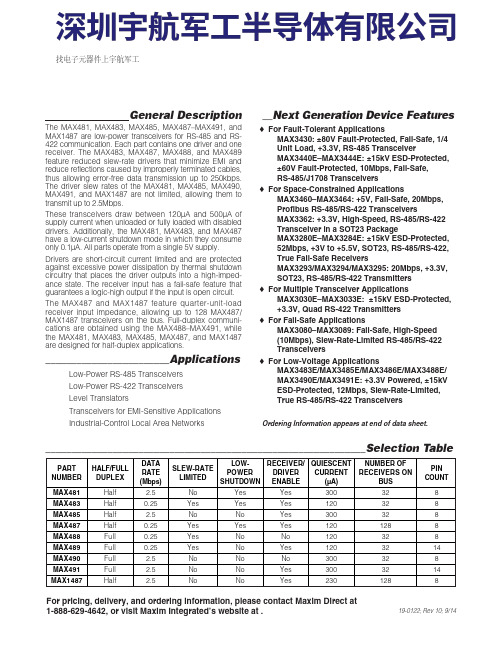
General DescriptionThe MAX481, MAX483, MAX485, MAX487–MAX491, andMAX1487 are low-power transceivers for RS-485 and RS-422 communication. Each part contains one driver and onereceiver. The MAX483, MAX487, MAX488, and MAX489feature reduced slew-rate drivers that minimize E MI andreduce reflections caused by improperly terminated cables,thus allowing error-free data transmission up to 250kbps.The driver slew rates of the MAX481, MAX485, MAX490,MAX491, and MAX1487 are not limited, allowing them totransmit up to 2.5Mbps.These transceivers draw between 120µA and 500µA ofsupply current when unloaded or fully loaded with disableddrivers. Additionally, the MAX481, MAX483, and MAX487have a low-current shutdown mode in which they consumeonly 0.1µA. All parts operate from a single 5V supply.Drivers are short-circuit current limited and are protectedagainst excessive power dissipation by thermal shutdowncircuitry that places the driver outputs into a high-imped-ance state. The receiver input has a fail-safe feature thatguarantees a logic-high output if the input is open circuit.The MAX487 and MAX1487 feature quarter-unit-loadreceiver input impedance, allowing up to 128 MAX487/MAX1487 transceivers on the bus. Full-duplex communi-cations are obtained using the MAX488–MAX491, whilethe MAX481, MAX483, MAX485, MAX487, and MAX1487are designed for half-duplex applications.________________________Applications Low-Power RS-485 Transceivers Low-Power RS-422 Transceivers Level Translators Transceivers for EMI-Sensitive Applications Industrial-Control Local Area Networks__Next Generation Device Features o For Fault-Tolerant Applications MAX3430: ±80V Fault-Protected, Fail-Safe, 1/4Unit Load, +3.3V, RS-485 Transceiver MAX3440E–MAX3444E: ±15kV ESD-Protected,±60V Fault-Protected, 10Mbps, Fail-Safe, RS-485/J1708 Transceivers o For Space-Constrained Applications MAX3460–MAX3464: +5V, Fail-Safe, 20Mbps,Profibus RS-485/RS-422 Transceivers MAX3362: +3.3V, High-Speed, RS-485/RS-422Transceiver in a SOT23 Package MAX3280E–MAX3284E: ±15kV ESD-Protected,52Mbps, +3V to +5.5V, SOT23, RS-485/RS-422,True Fail-Safe Receivers MAX3293/MAX3294/MAX3295: 20Mbps, +3.3V,SOT23, RS-485/RS-422 Transmitters o For Multiple Transceiver Applications MAX3030E–MAX3033E: ±15kV ESD-Protected,+3.3V, Quad RS-422 Transmitters o For Fail-Safe Applications MAX3080–MAX3089: Fail-Safe, High-Speed (10Mbps), Slew-Rate-Limited RS-485/RS-422Transceiverso For Low-Voltage ApplicationsMAX3483E/MAX3485E/MAX3486E/MAX3488E/MAX3490E/MAX3491E: +3.3V Powered, ±15kVESD-Protected, 12Mbps, Slew-Rate-Limited,True RS-485/RS-422 Transceivers For pricing, delivery, and ordering information, please contact Maxim Direct at1-888-629-4642, or visit Maxim Integrated’s website at .______________________________________________________________Selection Table19-0122; Rev 10; 9/14PARTNUMBERHALF/FULL DUPLEX DATA RATE (Mbps) SLEW-RATE LIMITED LOW-POWER SHUTDOWN RECEIVER/DRIVER ENABLE QUIESCENT CURRENT (μA) NUMBER OF RECEIVERS ON BUS PIN COUNT MAX481Half 2.5No Yes Yes 300328MAX483Half 0.25Yes Yes Yes 120328MAX485Half 2.5No No Yes 300328MAX487Half 0.25Yes Yes Yes 1201288MAX488Full 0.25Yes No No 120328MAX489Full 0.25Yes No Yes 1203214MAX490Full 2.5No No No 300328MAX491Full 2.5No No Yes 3003214MAX1487 Half 2.5No No Yes 2301288Ordering Information appears at end of data sheet.找电子元器件上宇航军工MAX481/MAX483/MAX485/MAX487–MAX491/MAX1487Low-Power, Slew-Rate-LimitedRS-485/RS-422 TransceiversPackage Information For the latest package outline information and land patterns, go to . Note that a “+”, “#”, or “-”in the package code indicates RoHS status only. Package drawings may show a different suffix character, but the drawing pertains to the package regardless of RoHS status.16Low-Power, Slew-Rate-Limited RS-485/RS-422 TransceiversMAX481/MAX483/MAX485/MAX487–MAX491/MAX1487Maxim Integrated cannot assume responsibility for use of any circuitry other than circuitry entirely embodied in a Maxim Integrated product. No circuit patent licenses are implied. Maxim Integrated reserves the right to change the circuitry and specifications without notice at any time. The parametric values (min and max limits) shown in the Electrical Characteristics table are guaranteed. Other parametric values quoted in this data sheet are provided for guidance.Maxim Integrated 160 Rio Robles, San Jose, CA 95134 USA 1-408-601-100017©2014 Maxim Integrated Products, Inc.Maxim Integrated and the Maxim Integrated logo are trademarks of Maxim Integrated Products, Inc.。

MAX3222E/MAX3232E/MAX3237E/MAX3241E†/ MAX3246E的中文芯片手册±15kV ESD保护,电流低至10nA,3.0V至5.5V,高达1Mbps,的RS-232收发器概述该MAX3222E/MAX3232E/MAX3237E/MAX3241E /MAX3246E +3.0 V供电EIA/TIA-232和V.28/V.24通信接口器件具有低功耗,高数据速率的能力,以及增强的静电放电(ESD)保护。
增强型ESD结构保护所有发送器输出和接收器输入采用IEC 1000-4-2气隙放电,±8kV使用IEC 1000-4-2接触放电(MAX3246E为±9kV ),±15kV使用人体模型。
基于上述标准,MAX3237E的逻辑和接收I / O 引脚将被保护,而发射机输出引脚的保护利用人体模型±15kV的。
一个专有的低压差发送器输出级可以提供+3.0 V至+5.5 V电源真正的RS -232性能,利用内部双电荷泵。
充电泵仅需要四个工作在+3.3 V电源的0.1μF的小电容。
每款器件保证工作在250kbps数据速率下维持RS - 232输出电平。
该MAX3237E保证操作在250kbps在正常工作模式和1Mbps的中MegaBaud™工作模式,同时保持RS- 232兼容的输出电平。
MAX3222E/MAX3232E包括两个接收器和两个发射器。
MAX3222E具有1μA关断模式,可降低功耗的电池供电的便携式系统。
该MAX3222E接收器仍活跃在关断模式下,允许监控外部设备的同时仅需耗电1μA供应电流。
TheMAX3222E和MAX3232E的引脚,封装,并与业界标准的MAX242和MAX232,分别为功能兼容。
该MAX3241E/MAX3246E是专为笔记本电脑和小型笔记本电脑设计完整串口(3个驱动器/5个接收器)。
该MAX3237E(5驱动器/ 三个接收器),非常适合那些需要快速数据传输的外围设备。

MAX3485ESA品牌厂家:Maxim Integrated(美信),MAX3485ESA 渠道分销商:2家,现货库存数量:1542 PCS,MAX3485ESA价格参考:¥8.042元。
Maxim Integrated(美信)MAX3485ESA参数(SOIC 8Pin 3V 10Mbps,封装:SOIC),MAX3485ESA中文资料和引脚图及功能表说明书PDF下载(17页,409KB),您可以在MAX3485ESA接口芯片规格书Datesheet数据手册中,查到MAX3485ESA引脚图及功能的应用电路图电压和使用方法,MAX3485ESA典型电路教程。
MAX3485ESA可以用什么代替?代换型号如:MAX3485CSA+T、MAX3485CSA替代换,MAX3485ESA芯片系列中文手册中包含MAX3485ESA各引脚定义说明介绍及MAX3485ESA引脚功能图解,用户中文手册MAX3485ESA芯片手册PDF下载(17页,409KB)。
您可在采芯网下载MAX3485ESA产品选型手册,MAX3485ESA产品设计参考手册,MAX3485ESA用户编程技术手册,MAX3485ESA开发手册(3个文件)。
MAX3485ESA 代替型号更多代替型号器件图型号制造商品名代替类型描述对比MAX3485ESASOIC 8Pin 3V 10MbpsMaxim Integrated (美信)接口芯片当前型号3.3V供电,10Mbps的和摆率限制真RS - 485 / RS -422收发器3.3V-Powered, 10Mbps and Slew-Rate-Limited True RS-485/RS-422 Transceivers当前型号MAX3485CSA+TNSOIC 8Pin 3V接口芯片完全替代MAXIM INTEGRATED PRODUCTS MAX3485CSA+T 芯片, RS422/RS485 收发器, 10MBPS, 3.6V, NSOIC-8MAX3485ESA和MAX3485CSA+T区别MAX3485CSANSOIC 8Pin 3V 10Mbps美信接口芯片完全替代3.3V供电,10Mbps的和摆率限制真RS - 485 / RS -422收发器3.3V-Powered, 10Mbps and Slew-Rate-Limited True RS-485/RS-422 TransceiversMAX3485ESA和MAX3485CSA区别SN75HVD11DRSOIC 8Pin德州仪器接口芯片类似代替3.3 V RS - 485收发器3.3-V RS-485 TRANSCEIVERS MAX3485ESA和SN75HVD11DR区别MAX3485ESA 相关器件器件图型号制造商品名封装描述价格(RMB)PDFSN65HVD1780DRSOIC 8Pin 3.3V德州仪器接口芯片SOIC, PDIPTEXAS INSTRUMENTS SN65HVD1780DR 芯片, 收发器, RS-485, 10MBPS, SOIC-8, 整卷¥ 6.637ISL83485IBZ-TSOIC 8Pin 3.6V 10Mbps英特矽尔接口芯片SOICRS-485 线路驱动器和接收器,Intersil 可靠的数据传输应用,使用长双绞线连接,带Intersil 半双工和全双工RS - 485 收发器,提供各种速度等级。


(V CC = +3.3V, T A = +25°C)Note 1: ∆V OD and ∆V OC are the changes in V OD and V OC , respectively, when the DI input changes state.Note 2: Measured on |t PLH (Y) - t PHL (Y)| and |t PLH (Z) - t PHL (Z)|.Note 3: The transceivers are put into shutdown by bringing RE high and DE low. If the inputs are in this state for less than 80ns, the parts are guaranteed not to enter shutdown. If the inputs are in this state for at least 300ns, the parts are guaranteed tohave entered shutdown. See Low-Power Shutdown Mode section.PARAMETERSYMBOL CONDITIONS MIN TYP MAX UNITS Time to Shutdownt SHDN MAX3483E/MAX3485E/MAX3486E/MAX3491E only (Note 3)80190300ns Receiver Propagation Delay,Low-to-High Levelt RPLH V ID = 0 to 3.0, C L = 15pF, Figure 11256290ns MAX3483E/MAX3488E 2575120Receiver Propagation Delay,High-to-Low Levelt RPHL V ID = 0 to 3.0, C L = 15pF, Figure 11256290ns MAX3483E/MAX3488E 2575120|t PLH - t PHL | ReceiverPropagation Delay Skewt RPDS V ID = 0 to 3.0, C L = 15pF, Figure 116±10ns MAX3483E/MAX3488E 12±20Receiver Output Enable Timeto Low Levelt PRZL C L = 15pF, Figure 12,MAX3483E/85E/86E/91E only 2550ns Receiver Output Enable Timeto High Levelt PRZH C L = 15pF, Figure 12,MAX3483E/85E/86E/91E only 2550ns Receiver Output DisableTime from High Levelt PRHZ C L = 15pF, Figure 12,MAX3483E/85E/86E/91E only 2545ns Receiver Output DisableTime from Low Levelt PRLZ C L = 15pF, Figure 12,MAX3483E/85E/86E/91E only 2545ns Receiver Output Enable Timefrom Shutdown to Low Levelt PRSL C L = 15pF, Figure 12,MAX3483E/85E/86E/91E only 7201400ns Receiver Output Enable Timefrom Shutdown to High Level t PRSH C L = 15pF, Figure 12,MAX3483E/85E/86E/91E only 7201400nsMAX3483E/MAX3485E/MAX3486E/MAX3488E/MAX3490E/MAX3491E3.3V-Powered, ±15kV ESD-Protected, 12Mbps and Slew-Rate-Limited True RS-485/RS-422 Transceivers Receiver Switching CharacteristicsFigure 24. MAX3483E/MAX3485E/MAX3486E Typical RS-485 NetworkFigure 25. MAX3488E/MAX3490E/MAX3491E Full-Duplex RS-485 NetworkMAX3483E/MAX3485E/MAX3486E/MAX3488E/MAX3490E/MAX3491E3.3V-Powered, ±15kV ESD-Protected, 12Mbps and Slew-Rate-Limited True RS-485/RS-422 Transceivers。