74HC04D-T中文资料
- 格式:pdf
- 大小:115.54 KB
- 文档页数:20
![74HC04和74HC14的区别(施密特触发的作用)[大全五篇]](https://uimg.taocdn.com/8e0c3d8bf021dd36a32d7375a417866fb84ac00c.webp)
74HC04和74HC14的区别(施密特触发的作用)[大全五篇]第一篇:74HC04和74HC14的区别(施密特触发的作用)74HC04和74HC14的具体区别详解同样具有反相器功能,你知道74HC04和74HC14的具体区别吗?对于74HC04很好理解,输入低电平,输出高电平;输入高电平,输出低电平。
可是具体到几伏电压算高电平,几伏算低电平呢?答案是看手册。
下图是TI的74HC04的输入特性表,举个例子来看,当芯片供电电压Vcc=4.5V时,输入端最少输入3.15V电压才可以被74HC04识别为高电平;同理,输入端只有输入不大于1.35V的电压,才可以被识别为低电平。
下图是74HC04的输出特性表,在TEST CONDITIONS(测试条件)分别选IOH=-4mA和IOL=4mA,再举例子看,同上面的一样,当芯片供电电压Vcc=4.5V时,且输入端被识别为低电平,输出端VOH就是高电平,且最小值为3.84V;同理,当芯片供电电压Vcc=4.5V时,且输入端被识别为高电平,输出端VOL就是低电平,且最大值为0.33V。
从以上的分析可以看出,经74HC04的反相,到底输出几伏的高电平或低电平主要和该芯片的供电电压关系密切!以上对于74HC04的分析同样适用于74HC14!关于以上的数据,他们在手册中完全一样!也就是单纯作为反相器使用时,可以通用。
但是74HC14除了反相器这个基本功能外,他还是个施密特触发器。
关于什么是施密特触发器,现用一个图简单介绍:对于74HC14来说,当输入VI大于阀值电压VT+时,输出VO由高电平变低电平;当输入VI小于阀值电压VT-时,输出VO由低电平变高电平;通过上面分析,我们了解了施密特触发器是以反相器为基础的,以及阀值电压的基本概念。
下面来看一下74HC14这个施密特触发器的手册数据:VOH和VOL上文已经介绍过了,下面看一下VT+和VT-:当芯片供电电压Vcc=4.5V时,正向阀值的典型值VT+=2.5V,负向阀值的典型值VT-=1.6V。
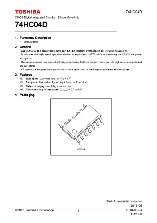
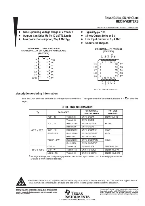
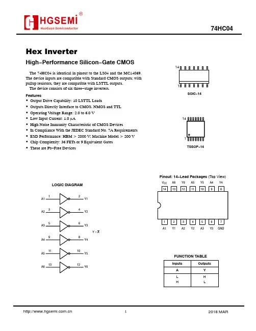
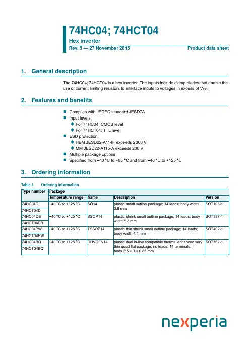
74HC04的作用:6位反相器。
第7脚GND ,电源地。
第14脚VCC ,电源正极。
信号由A 端输入Y 端反相输出,A1与Y1为一组,其它类推。
例:A1=“1”则Y1=“0”、A1=“0”则Y1=“1”,其它组功能一样。
74HC138的作用:八位二进制译十进制译码器。
第8脚GND ,电源地。
第15脚VCC ,电源正极第1~3脚A 、B 、C ,二进制输入脚。
第4~6脚片选信号控制,只有在4、5脚为“0”6脚为“1”时,才会被选通,输出受A 、B 、C 信号控制。
其它任何组合方式将不被选通,且Y0~Y7输出全为“1”。
通过控制选通脚来级联,使之扩展到十六位。
例:G2A=0,G2B=0,G1=1,A=1,B=0,C=0,则Y0为“0”Y1~Y7为“1”。
74HC595的作用:LED 驱动芯片,8位移位锁存器。
第8脚GND ,电源地。
第16脚VCC ,电源正极第14脚DATA ,串行数据输入口,显示数据由此进入,必须有时钟信号的配合才能移入。
第13脚EN ,使能口,当该引脚上为“1”时QA~QH口全部为“1”,为“0”时QA~QH的输出由输入的数据控制。
第12脚STB ,锁存口,当输入的数据在传入寄存器后,只有供给一个锁存信号才能将移入的数据送QA~QH口输出。
第11脚CLK ,时钟口,每一个时钟信号将移入一位数据到寄存器。
第10脚SCLR ,复位口,只要有复位信号,寄存器内移入的数据将清空,显示屏不用该脚,一般接VCC 。
第9脚DOUT ,串行数据输出端,将数据传到下一个。
第15、1~7脚,并行输出口也就是驱动输出口,驱动LED 。
4953的作用:行驱动管,功率管。
其内部是两个CMOS 管,1、3脚VCC ,2、4脚控制脚,2脚控制7、8脚的输出,4脚控制5、6脚的输出,只有当2、4脚为“0”时,7、8、5、6才会输出,否则输出为高阻状态。
TB62726的作用:LED 驱动芯片,16位移位锁存器。
PACKAGING INFORMATIONOrderable DeviceStatus (1)Package Type Package Drawing Pins Package Qty Eco Plan (2)Lead/Ball FinishMSL Peak Temp (3)86010012A ACTIVE LCCC FK 201TBD Call TI N /A for Pkg Type 8601001CA ACTIVE CDIP J 141TBD Call TI N /A for Pkg Type SN54HCU04J ACTIVE CDIP J 141TBDCall TI N /A for Pkg Type SN74HCU04D ACTIVE SOIC D 1450Green (RoHS &no Sb/Br)CU NIPDAU Level-1-260C-UNLIM SN74HCU04DBR ACTIVE SSOP DB 142000Green (RoHS &no Sb/Br)CU NIPDAU Level-1-260C-UNLIM SN74HCU04DBRE4ACTIVE SSOP DB 142000Green (RoHS &no Sb/Br)CU NIPDAU Level-1-260C-UNLIM SN74HCU04DE4ACTIVE SOIC D 1450Green (RoHS &no Sb/Br)CU NIPDAU Level-1-260C-UNLIM SN74HCU04DR ACTIVE SOIC D 142500Green (RoHS &no Sb/Br)CU NIPDAU Level-1-260C-UNLIM SN74HCU04DRE4ACTIVE SOIC D 142500Green (RoHS &no Sb/Br)CU NIPDAU Level-1-260C-UNLIM SN74HCU04DT ACTIVE SOIC D 14250Green (RoHS &no Sb/Br)CU NIPDAU Level-1-260C-UNLIM SN74HCU04DTE4ACTIVE SOIC D 14250Green (RoHS &no Sb/Br)CU NIPDAU Level-1-260C-UNLIM SN74HCU04N ACTIVE PDIP N 1425Pb-Free (RoHS)CU NIPDAU N /A for Pkg Type SN74HCU04N3OBSOLETE PDIP N 14TBD Call TI Call TISN74HCU04NE4ACTIVE PDIP N 1425Pb-Free (RoHS)CU NIPDAU N /A for Pkg Type SN74HCU04NSR ACTIVE SO NS 142000Green (RoHS &no Sb/Br)CU NIPDAU Level-1-260C-UNLIM SN74HCU04NSRE4ACTIVE SO NS 142000Green (RoHS &no Sb/Br)CU NIPDAU Level-1-260C-UNLIM SN74HCU04PW ACTIVE TSSOP PW 1490Green (RoHS &no Sb/Br)CU NIPDAU Level-1-260C-UNLIM SN74HCU04PWE4ACTIVE TSSOP PW 1490Green (RoHS &no Sb/Br)CU NIPDAU Level-1-260C-UNLIM SN74HCU04PWR ACTIVE TSSOP PW 142000Green (RoHS &no Sb/Br)CU NIPDAU Level-1-260C-UNLIM SN74HCU04PWRE4ACTIVE TSSOP PW 142000Green (RoHS &no Sb/Br)CU NIPDAU Level-1-260C-UNLIM SN74HCU04PWT ACTIVE TSSOP PW 14250Green (RoHS &no Sb/Br)CU NIPDAU Level-1-260C-UNLIM SN74HCU04PWTE4ACTIVE TSSOP PW 14250Green (RoHS &no Sb/Br)CU NIPDAU Level-1-260C-UNLIM SNJ54HCU04FK ACTIVE LCCC FK 201TBD Call TI N /A for Pkg Type SNJ54HCU04JACTIVECDIPJ141TBDCall TIN /A for Pkg Type(1)The marketing status values are defined as follows:ACTIVE:Product device recommended for new designs.LIFEBUY:TI has announced that the device will be discontinued,and a lifetime-buy period is in effect.NRND:Not recommended for new designs.Device is in production to support existing customers,but TI does not recommend using this part in a new design.PREVIEW:Device has been announced but is not in production.Samples may or may not be available.OBSOLETE:TI has discontinued the production of the device.12-Jan-2006(2)Eco Plan -The planned eco-friendly classification:Pb-Free (RoHS),Pb-Free (RoHS Exempt),or Green (RoHS &no Sb/Br)-please check /productcontent for the latest availability information and additional product content details.TBD:The Pb-Free/Green conversion plan has not been defined.Pb-Free (RoHS):TI's terms "Lead-Free"or "Pb-Free"mean semiconductor products that are compatible with the current RoHS requirements for all 6substances,including the requirement that lead not exceed 0.1%by weight in homogeneous materials.Where designed to be soldered at high temperatures,TI Pb-Free products are suitable for use in specified lead-free processes.Pb-Free (RoHS Exempt):This component has a RoHS exemption for either 1)lead-based flip-chip solder bumps used between the die and package,or 2)lead-based die adhesive used between the die and leadframe.The component is otherwise considered Pb-Free (RoHS compatible)as defined above.Green (RoHS &no Sb/Br):TI defines "Green"to mean Pb-Free (RoHS compatible),and free of Bromine (Br)and Antimony (Sb)based flame retardants (Br or Sb do not exceed 0.1%by weight in homogeneous material)(3)MSL,Peak Temp.--The Moisture Sensitivity Level rating according to the JEDEC industry standard classifications,and peak solder temperature.Important Information and Disclaimer:The information provided on this page represents TI's knowledge and belief as of the date that it is provided.TI bases its knowledge and belief on information provided by third parties,and makes no representation or warranty as to the accuracy of such information.Efforts are underway to better integrate information from third parties.TI has taken and continues to take reasonable steps to provide representative and accurate information but may not have conducted destructive testing or chemical analysis on incoming materials and chemicals.TI and TI suppliers consider certain information to be proprietary,and thus CAS numbers and other limited information may not be available for release.In no event shall TI's liability arising out of such information exceed the total purchase price of the TI part(s)at issue in this document sold by TI to Customer on an annualbasis.12-Jan-2006IMPORTANT NOTICETexas Instruments Incorporated and its subsidiaries (TI) reserve the right to make corrections, modifications, enhancements, improvements, and other changes to its products and services at any time and to discontinue any product or service without notice. Customers should obtain the latest relevant information before placing orders and should verify that such information is current and complete. All products are sold subject to TI’s terms and conditions of sale supplied at the time of order acknowledgment.TI warrants performance of its hardware products to the specifications applicable at the time of sale in accordance with TI’s standard warranty. Testing and other quality control techniques are used to the extent TI deems necessary to support this warranty. Except where mandated by government requirements, testing of all parameters of each product is not necessarily performed.TI assumes no liability for applications assistance or customer product design. Customers are responsible for their products and applications using TI components. To minimize the risks associated with customer products and applications, customers should provide adequate design and operating safeguards.TI does not warrant or represent that any license, either express or implied, is granted under any TI patent right, copyright, mask work right, or other TI intellectual property right relating to any combination, machine, or process in which TI products or services are used. Information published by TI regarding third-party products or services does not constitute a license from TI to use such products or services or a warranty or endorsement thereof. Use of such information may require a license from a third party under the patents or other intellectual property of the third party, or a license from TI under the patents or other intellectual property of TI. Reproduction of information in TI data books or data sheets is permissible only if reproduction is without alteration and is accompanied by all associated warranties, conditions, limitations, and notices. Reproduction of this information with alteration is an unfair and deceptive business practice. TI is not responsible or liable for such altered documentation.Resale of TI products or services with statements different from or beyond the parameters stated by TI for that product or service voids all express and any implied warranties for the associated TI product or service and is an unfair and deceptive business practice. TI is not responsible or liable for any such statements. Following are URLs where you can obtain information on other Texas Instruments products and application solutions:Products ApplicationsAmplifiers Audio /audioData Converters Automotive /automotiveDSP Broadband /broadband Interface Digital Control /digitalcontrolLogic Military /militaryPower Mgmt Optical Networking /opticalnetwork Microcontrollers Security /securityTelephony /telephonyVideo & Imaging /videoWireless /wirelessMailing Address:Texas InstrumentsPost Office Box 655303 Dallas, Texas 75265Copyright 2006, Texas Instruments Incorporated。
Hex InverterHigh −Performance Silicon −Gate CMOSThe 74HC04 is identical in pinout to the LS04 and the MC14069.The device inputs are compatible with Standard CMOS outputs; with pullup resistors, they are compatible with LSTTL outputs.The device consists of six three −stage inverters.Features•Output Drive Capability: 10 LSTTL Loads•Outputs Directly Interface to CMOS, NMOS and TTL •Operating V oltage Range: 2.0 to 6.0 V •Low Input Current: 1.0 m A•High Noise Immunity Characteristic of CMOS Devices•In Compliance With the JEDEC Standard No. 7A Requirements •ESD Performance: HBM > 2000 V; Machine Model > 200 V •Chip Complexity: 36 FETs or 9 Equivalent Gates •These are Pb −Free DevicesLOGIC DIAGRAMY1A1A2A3A4A5A6Y2Y3Y4Y5Y6Y = APinout: 14−Lead Packages (Top View)1314121110982134567V CC A6Y6A5Y5A4Y4A1Y1A2Y2A3Y3GNDTSSOP −14SOIC −14114114L HFUNCTION TABLEInputsOutputsA H LYMAXIMUM RATINGSSymbol Parameter Value Unit V CC DC Supply Voltage (Referenced to GND)– 0.5 to + 7.0V V in DC Input Voltage (Referenced to GND)– 0.5 to V CC + 0.5V V out DC Output Voltage (Referenced to GND)– 0.5 to V CC + 0.5VI in DC Input Current, per Pin±20mAI out DC Output Current, per Pin±25mAI CC DC Supply Current, V CC and GND Pins±50mAP D Power Dissipation in Still Air,SOIC Package†TSSOP Package†500450mWT stg Storage Temperature– 65 to + 150_C T L Lead Temperature, 1 mm from Case for 10 SecondsSOIC or TSSOP Package260_CStresses exceeding Maximum Ratings may damage the device. Maximum Ratings are stress ratings only. Functional operation above the Recommended Operating Conditions is not implied. Extended exposure to stresses above the Recommended Operating Conditions may affect device reliability.*This device contains protection circuitry to guard against damage due to high static voltages or electric fields. However, precautions must be taken to avoid applications of any voltage higher than maximum rated voltages to this high−impedance circuit. For proper operation, V in and V out should be constrained to the range GND v (V in or V out) v V CC. Unused inputs must always be tied to an appropriate logic voltage level (e.g., either GND or V CC). Unused outputs must be left open.†Derating−SOIC Package: – 7 mW/_C from 65_ to 125_CTSSOP Package: − 6.1 mW/_C from 65_ to 125_CFor high frequency or heavy load considerations, see Chapter 2 of the ON Semiconductor High−Speed CMOS Data Book (DL129/D).RECOMMENDED OPERATING CONDITIONSSymbol Parameter Min Max Unit V CC DC Supply Voltage (Referenced to GND) 2.0 6.0VV in, V out DC Input Voltage, Output Voltage (Referenced to GND)0V CC V T A Operating Temperature, All Package Types– 55+ 125_Ct r, t f Input Rise and Fall Time V CC = 2.0 V (Figure 1)V CC = 4.5 VV CC = 6.0 V 01000500400nsDC CHARACTERISTICS(Voltages Referenced to GND)V CC (V)Guaranteed LimitSymbol Parameter Condition−55 to 25°C≤85°C≤125°C UnitV IH Minimum High−Level InputVoltage V out = 0.1V or V CC−0.1V|I out| ≤ 20m A2.03.04.56.01.502.103.154.201.502.103.154.201.502.103.154.20VV IL Maximum Low−Level InputVoltage V out = 0.1V or V CC− 0.1V|I out| ≤ 20m A2.03.04.56.00.500.901.351.800.500.901.351.800.500.901.351.80VV OH Minimum High−Level OutputVoltage V in = V IH or V IL|I out| ≤ 20m A2.04.56.01.94.45.91.94.45.91.94.45.9V V in =V IH or V IL|I out| ≤ 2.4mA|I out| ≤ 4.0mA |I out| ≤ 5.2mA 3.04.56.02.483.985.482.343.845.342.203.705.20V OL Maximum Low−Level OutputVoltage V in = V IH or V IL|I out| ≤ 20m A2.04.56.00.10.10.10.10.10.10.10.10.1VV in = V IH or V IL|I out| ≤ 2.4mA|I out| ≤ 4.0mA|I out| ≤ 5.2mA3.04.56.00.260.260.260.330.330.330.400.400.40I in Maximum Input LeakageCurrentV in = V CC or GND 6.0±0.1±1.0±1.0m AI CC Maximum Quiescent SupplyCurrent (per Package)V in = V CC or GNDI out = 0m A6.0 2.02040m ANOTE:Information on typical parametric values can be found in Chapter 2 of the ON Semiconductor High−Speed CMOS Data Book (DL129/D). AC CHARACTERISTICS(C L = 50pF, Input t r = t f = 6ns)V CC (V)Guaranteed LimitSymbol Parameter−55 to 25°C≤85°C≤125°C Unitt PLH, t PHL Maximum Propagation Delay, Input A or B to Output Y(Figures 1 and 2)2.03.04.56.07530151395401916110552219nst TLH, t THL Maximum Output Transition Time, Any Output(Figures 1 and 2)2.03.04.56.07527151395321916110362219nsC in Maximum Input Capacitance101010pF NOTE:For propagation delays with loads other than 50 pF, and information on typical parametric values, see Chapter 2 of the ON Semiconductor High−Speed CMOS Data Book (DL129/D).C PD Power Dissipation Capacitance (Per Inverter)*Typical @ 25°C, V CC = 5.0 VpF20*Used to determine the no−load dynamic power consumption: P D = C PD V CC2f + I CC V CC. For load considerations, see Chapter 2 of the ON Semiconductor High−Speed CMOS Data Book (DL129/D).Figure 1. Switching WaveformsGNDV CCOUTPUT YINPUT AC L **Includes all probe and jig capacitanceTESTFigure 2. Test CircuitYA Figure 3. Expanded Logic Diagram(1/6 of the Device Shown)。
74HCT04Hex InverterWith LSTTL−Compatible InputsHigh−Performance Silicon−Gate CMOSThe 74HCT04 may be used as a level converter for interfacing TTL or NMOS outputs to High−Speed CMOS inputs. The HCT04A is identical in pinout to the LS04.Features•Output Drive Capability: 10 LSTTL Loads•TTL/NMOS−Compatible Input Levels•Outputs Directly Interface to CMOS, NMOS and TTL •Operating V oltage Range: 4.5 to 5.5 V•Low Input Current: 1.0 m A•In Compliance With the JEDEC Standard No. 7A Requirements •ESD Performance: HBM > 2000 V; Machine Model > 200 V •Chip Complexity: 48 FETs or 12 Equivalent Gates•These are Pb−Free DevicesMARKINGDIAGRAMSHCT04= Device CodeA= Assembly LocationL, WL= Wafer LotY= YearW, WW= Work WeekG or G= Pb−Free PackageTSSOP−14DT SUFFIXCASE 948GSOIC−14D SUFFIXCASE 751AHCT04ALYW GG114See detailed ordering and shipping information in the package dimensions section on page 2 of this data sheet.ORDERING INFORMATION(Note: Microdot may be in either location)LOGIC DIAGRAMY1A1A2A3A4A5A6Y2Y3Y4Y5Y6Y = APin 14 = V CC Pin 7 = GNDPinout: 14−Lead Packages (Top View)1314121110982134567V CC A6Y6A5Y5A4Y4A1Y1A2Y2A3Y3GNDL HFUNCTION TABLEInputs OutputsA H LY ORDERING INFORMATIONDevicePackage Shipping †74HCT04DR2G SOIC −14(Pb −Free)2500 / Tape & Reel74HCT04DTR2GTSSOP −14*†For information on tape and reel specifications, including part orientation and tape sizes, please refer to our Tape and Reel Packaging Specifications Brochure, BRD8011/D.*This package is inherently Pb −Free.MAXIMUM RATINGSSymbol ParameterValue Unit V CC DC Supply Voltage (Referenced to GND)– 0.5 to + 7.0V V in DC Input Voltage (Referenced to GND)– 0.5 to V CC + 0.5V V out DC Output Voltage (Referenced to GND)– 0.5 to V CC + 0.5V I in DC Input Current, per Pin ±20mA I out DC Output Current, per Pin±25mA I CC DC Supply Current, V CC and GND Pins ±50mA P D Power Dissipation in Still Air SOIC Package†TSSOP Package†500450mW T stg Storage Temperature Range– 65 to + 150_C T LLead Temperature, 1 mm from Case for 10 SecondsSOIC or TSSOP Package260_CStresses exceeding Maximum Ratings may damage the device. Maximum Ratings are stress ratings only. Functional operation above the Recommended Operating Conditions is not implied.Extended exposure to stresses above the Recommended Operating Conditions may affect device reliability.†Derating —SOIC Package: – 7 mW/_C from 65_ to 125_CTSSOP Package: − 6.1 mW/_C from 65_ to 125_CFor high frequency or heavy load considerations, see Chapter 2 of the ON Semiconductor High −Speed CMOS Data Book (DL129/D).RECOMMENDED OPERATING CONDITIONSSymbol ParameterMin Max Unit V CC DC Supply Voltage (Referenced to GND)4.55.5V V in , V outDC Input Voltage, Output Voltage (Referenced to GND)0V CC V T A Operating Temperature Range, All Package Types – 55+ 125_C t r , t fInput Rise/Fall Time (Figure 1)500nsDC CHARACTERISTICS (Voltages Referenced to GND)V CC (V)Guaranteed LimitSymbol ParameterCondition−55 to 25°C≤85°C ≤125°C Unit V IH Minimum High −Level Input Voltage V out = 0.1V |I out | ≤ 20m A 4.55.5 2.02.0 2.02.0 2.02.0V V IL Maximum Low −Level Input Voltage V out = V CC − 0.1V |I out | ≤ 20m A 4.55.50.80.80.80.80.80.8V V OHMinimum High −Level Output VoltageV in = V IL |I out | ≤ 20m A 4.55.5 4.45.4 4.45.4 4.45.4VV in = V IL|I out | ≤ 4.0mA4.5 3.98 3.84 3.70V OLMaximum Low −Level Output VoltageV in = V IH |I out | ≤ 20m A 4.55.50.10.10.10.10.10.1V V in = V IH|I out | ≤ 4.0mA 4.50.260.330.40I in Maximum Input Leakage Current V in = V CC or GND 5.5±0.1±1.0±1.0m A I CCMaximum Quiescent Supply Current (per Package)V in = V CC or GND I out = 0m A5.52.02040m A D I CCAdditional Quiescent Supply CurrentV in = 2.4V, Any One InputV in = V CC or GND, Other Inputs I out = 0m A5.5≥ −55°C25 to 125°CmA2.92.4rmation on typical parametric values can be found in Chapter 2 of the ON Semiconductor High −Speed CMOS Data Book (DL129/D).2.Total Supply Current = I CC + ΣD I CC .This device contains protection circuitry to guard against damage due to high static voltages or electric fields. However, precautions must be taken to avoid applications of any voltage higher than maximum rated voltages to this high −impedance cir-cuit. For proper operation, V in and V out should be constrained to the range GND v (V in or V out ) v V CC .Unused inputs must always be tied to an appropriate logic voltage level (e.g., either GND or V CC ).Unused outputs must be left open.AC CHARACTERISTICS (V CC = 5.0V ±10%, C L = 50pF, Input t r = t f = 6ns)Guaranteed LimitSymbol Parameter−55 to 25°C≤85°C ≤125°C Unit t PLH ,t PHL Maximum Propagation Delay, Input A to Output Y (Figures 1 and 2)151719212226ns t TLH ,t THL Maximum Output Transition Time, Any Output (Figures 1 and 2)151922ns C inMaximum Input Capacitance101010pF3.For propagation delays with loads other than 50 pF, and information on typical parametric values, see Chapter 2 of the ON Semiconductor High −Speed CMOS Data Book (DL129/D).C PDPower Dissipation Capacitance (Per Inverter)*Typical @ 25°C, V CC = 5.0 VpF22*Used to determine the no −load dynamic power consumption: P D = C PD V CC 2f + I CC V CC . For load considerations, see Chapter 2 of the ON Semiconductor High −Speed CMOS Data Book (DL129/D).Figure 1. Switching Waveforms GND3.0VOUTPUT YINPUT AC L **Includes all probe and jig capacitanceTEST Figure 2. Test CircuitYA Figure 3. Expanded Logic Diagram(1/6 of the Device Shown)SOIC −14CASE 751A −03ISSUE HNOTES:1.DIMENSIONING AND TOLERANCING PER ANSI Y14.5M, 1982.2.CONTROLLING DIMENSION: MILLIMETER.3.DIMENSIONS A AND B DO NOT INCLUDE MOLD PROTRUSION.4.MAXIMUM MOLD PROTRUSION 0.15 (0.006)PER SIDE.5.DIMENSION D DOES NOT INCLUDE DAMBAR PROTRUSION. ALLOWABLE DAMBAR PROTRUSION SHALL BE 0.127(0.005) TOTAL IN EXCESS OF THE D DIMENSION AT MAXIMUM MATERIAL CONDITION.DIM MIN MAX MIN MAX INCHESMILLIMETERS A 8.558.750.3370.344B 3.80 4.000.1500.157C 1.35 1.750.0540.068D 0.350.490.0140.019F 0.40 1.250.0160.049G 1.27 BSC 0.050 BSC J 0.190.250.0080.009K 0.100.250.0040.009M 0 7 0 7 P 5.80 6.200.2280.244R0.250.500.0100.019____DIMENSIONS: MILLIMETERS*For additional information on our Pb −Free strategy and soldering details, please download the ON Semiconductor Soldering and Mounting Techniques Reference Manual, SOLDERRM/D.TSSOP −14CASE 948G −01ISSUE BDIM MIN MAX MIN MAX INCHESMILLIMETERS A 4.90 5.100.1930.200B 4.30 4.500.1690.177C −−− 1.20−−−0.047D 0.050.150.0020.006F 0.500.750.0200.030G 0.65 BSC 0.026 BSC H 0.500.600.0200.024J 0.090.200.0040.008J10.090.160.0040.006K 0.190.300.0070.012K10.190.250.0070.010L 6.40 BSC 0.252 BSC M0 8 0 8 NOTES:1.DIMENSIONING AND TOLERANCING PER ANSI Y14.5M, 1982.2.CONTROLLING DIMENSION: MILLIMETER.3.DIMENSION A DOES NOT INCLUDE MOLD FLASH, PROTRUSIONS OR GATE BURRS.MOLD FLASH OR GATE BURRS SHALL NOT EXCEED 0.15 (0.006) PER SIDE.4.DIMENSION B DOES NOT INCLUDE INTERLEAD FLASH OR PROTRUSION.INTERLEAD FLASH OR PROTRUSION SHALL NOT EXCEED 0.25 (0.010) PER SIDE.5.DIMENSION K DOES NOT INCLUDE DAMBAR PROTRUSION. ALLOWABLE DAMBAR PROTRUSION SHALL BE 0.08(0.003) TOTAL IN EXCESS OF THE K DIMENSION AT MAXIMUM MATERIAL CONDITION.6.TERMINAL NUMBERS ARE SHOWN FOR REFERENCE ONLY .7.DIMENSION A AND B ARE TO BE DETERMINED AT DATUM PLANE −W −.____14X REF K14X0.360.65PITCHSOLDERING FOOTPRINT**For additional information on our Pb −Free strategy and soldering details, please download the ON Semiconductor Soldering and Mounting Techniques Reference Manual, SOLDERRM/D.ON Semiconductor and are registered trademarks of Semiconductor Components Industries, LLC (SCILLC). SCILLC reserves the right to make changes without further notice to any products herein. SCILLC makes no warranty, representation or guarantee regarding the suitability of its products for any particular purpose, nor does SCILLC assume any liability arising out of the application or use of any product or circuit, and specifically disclaims any and all liability, including without limitation special, consequential or incidental damages.“Typical” parameters which may be provided in SCILLC data sheets and/or specifications can and do vary in different applications and actual performance may vary over time. All operating parameters, including “Typicals” must be validated for each customer application by customer’s technical experts. SCILLC does not convey any license under its patent rights nor the rights of others. SCILLC products are not designed, intended, or authorized for use as components in systems intended for surgical implant into the body, or other applications intended to support or sustain life, or for any other application in which the failure of the SCILLC product could create a situation where personal injury or death may occur. Should Buyer purchase or use SCILLC products for any such unintended or unauthorized application, Buyer shall indemnify and hold SCILLC and its officers, employees, subsidiaries, affiliates, and distributors harmless against all claims, costs, damages, and expenses, and reasonable attorney fees arising out of, directly or indirectly, any claim of personal injury or death associated with such unintended or unauthorized use, even if such claim alleges that SCILLC was negligent regarding the design or manufacture of the part. SCILLC is an Equal Opportunity/Affirmative Action Employer. This literature is subject to all applicable copyright laws and is not for resale in any manner.PUBLICATION ORDERING INFORMATION。
74hc04工作原理英文回答:The 74HC04 is a hex inverter gate, meaning that it has six independent inverters in a single package. Eachinverter takes a digital input signal and outputs the inverted (opposite) value. A logic inverter is a fundamental building block in digital logic circuits and performs the basic NOT operation.The 74HC04 is a TTL (Transistor-Transistor Logic) device, which means that it uses bipolar transistors to implement the logic functions. It is a member of the 74HC series, which is a high-speed CMOS (Complementary Metal-Oxide Semiconductor) family. CMOS devices are known for their low power consumption, high speed, and wide operating voltage range.The 74HC04 is a popular choice for inverting signals in a variety of applications, including:Logic level conversion.Signal conditioning.Buffering.Oscillator circuits.Switching circuits.The device is available in a variety of package options, including DIP (Dual In-Line Package), SOIC (Small Outline Integrated Circuit), and TSSOP (Thin Shrink Small Outline Package).中文回答:74HC04的工作原理。