MA2Q705中文资料
- 格式:pdf
- 大小:48.16 KB
- 文档页数:2
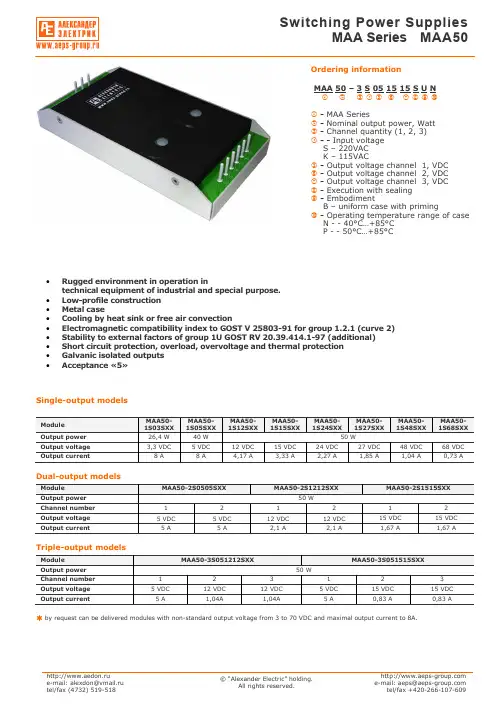
Single-output modelsModule МАА50- 1S03S ХХ МАА50- 1S05S ХХ МАА50- 1S12S ХХ МАА50- 1S15S ХХ МАА50- 1S24S ХХ МАА50- 1S27S ХХМАА50- 1S48S ХХ МАА50- 1S68S ХХ Output power 26,4 W 40 W 50 W Output voltage 3,3 VDC 5 VDC12 VDC15 VDC24 VDC27 VDC48 VDC68 VDCOutput current8 A8 А 4,17 А 3,33 А 2,27 А 1,85 А 1,04 А 0,73 АDual-output modelsModule МАА50-2S0505S ХХ МАА50-2S1212S ХХМАА50-2S1515S ХХOutput power 50 WChannel number 1 2 1 2 1 2 Output voltage 5 VDC 5 VDC 12 VDC 12 VDC15 VDC 15 VDC Output current5 А 5 А 2,1 А 2,1 А 1,67 А 1,67 АTriple-output modelsModule МАА50-3S051212S ХХМАА50-3S051515S ХХOutput power 50 WChannel number 1 2 3 1 2 3Output voltage 5 VDC12 VDC12 VDC5 VDC15 VDC15 VDCOutput current5 А 1,04А 1,04А 5 А 0,83 А 0,83 Аby request can be delivered modules with non-standard output voltage from 3 to 70 VDC and maximal output current to 8А.Ordering informationМАА 50 – 3 S 05 15 15 S U Nc d e f g h i j k lc - MAA Seriesd - Nominal output power, Watte - Channel quantity (1, 2, 3)f - - Input voltageS – 220VAC K – 115VACg - Output voltage channel 1, VDC h - Output voltage channel 2, VDC i - Output voltage channel 3, VDC j - Execution with sealing k - EmbodimentB – uniform case with primingl - Operating temperature range of caseN - - 40°С…+85°С P - - 50°С…+85°С• Rugged environment in operation intechnical equipment of industrial and special purpose. • Low-profile construction • Metal case• Cooling by heat sink or free air convection• Electromagnetic compatibility index to GOST V 25803-91 for group 1.2.1 (curve 2) • Stability to external factors of group 1U GOST RV 20.39.414.1-97 (additional) • Short circuit protection, overload, overvoltage and thermal protection • Galvanic isolated outputs •Acceptance «5»Температура окружающей среды Токр, С9080706050403020100-10-20-30-40-50Выходная мощность, Вт6050403020100Input specificationsParameter Conditions of dimensions MIN NOM MAX UnitS 187 220 242 VACSteady-state deviationК 80 115 140 VAC S 176 264 VACInput voltageTransient deflection, 1 secК 80 150 VAC SInput frequencyК47 400 440 HzOutput specificationsParameterConditions of dimensions MIN NOM MAX Unit Single-output execution (Inom 10 – 100%) ±3 % Output 1 multi-output execution(Inom 10 – 100%) ±3 %Uout2&3 differs from Uout1 less than 20% Output 2 and 3 multi-output execution(Inom 10 – 100%)±13 %Output 1 multi-output execution (Inom 30 – 100%) ±3 %Total output voltage instabilityUout2&3differs fromUout1 more than 20% Output 2 and 3 multi-output execution(Inom 50-100%) ±15 %Output voltage pulsations ripple(peak-to-peak)Dimension by device for pulsation control2% Uout.nom.Current overload protection actuation level110 % Iout.nom. Short circuit protection Autorepair 150 % Iout.nom. Overvoltage protection 120 % Uout.nom.Thermal protection90-95°CGeneral specificationsParameterConditions of dimensions MIN NOM MAX Unit- operating of case N P – 40 – 50 +85+85°C– power loss See diagram Temperature– storage – 50 +85 °CEfficiency 78 % Conversion frequency 50 kHz~ in/out 1500 VAC ~ in/case 1500 VAC~ out/case 500 VDC Isolation~ out/out 500 VDCInsulation resistance Voltage 500VDC 20 Ohm High humidity Temperature 35°С 98 % Cyclic overpatching of temperature – 60 +85 °C Multiple mechanical shocks Speeding-up 15g 2 15 ms Sinusoidal vibration Speeding-up 5g 50 500 Hz Atmosphere pressure 6х104 1,2х105 Pa Time to failure Temperature 35°C 105 hour Mass 0,4 kg all specifications redused for normal climatic conditions, Uin.nom., Iout.nom., if it is not specified differently.Power loss diagramFree airconvectionWith heat sinkAmbient temperature Tamb, °CO u t p u t p o w e r , WOutput settings№ pin1 2 3 4 5 6 7 8 9 Single-channel case ~IN (N) ~IN (L) +out1 +out1 +out1 -out1 -out1 -out1 Dual-channel case ~IN (N) ~IN (L) +out1 +out1 -out1 -out1 -out2 +out2 Triple-channelcase~IN (N)~IN (L)-out3+out3+out1-out1-out2+out2Switching on standart diagramFU in – current safety device 1A for input voltage 220VAC, 2A for input voltage 115VAC.S out – ceramic condenser capacity 0,47-15 mcF with corresponding operating voltage to decrease high-frequency noise level.S out2 – electronic condenser capacity 22-100 mcF in consideration with operating voltage and polarity. It makes for purpose to decrease dynamic instability when module work at dynamic load.+Out -Out ~In (L) ~In (N) Power module R heat CaseСout1 Сout2~In (L)~In (N)ground FU inSingle, Dual, and Triple-output execution SBNSingle, Dual, and Triple-output execution SVN (with flexible erection joints)The Flexible erection fjoints by length (100±5)mm is executed by wire section (0,5...1,5)mm2.。
5KE6V8(C)A - 1V5KE440(C)AV 8(C)A - 1 V5KE440(C)AV 8(C)A - 1 V5KE440(C)ADISCLAIMERFAIRCHILD SEMICONDUCTOR RESERVES THE RIGHT TO MAKE CHANGES WITHOUT FURTHER NOTICE TO ANY PRODUCTS HEREIN TO IMPROVE RELIABILITY , FUNCTION OR DESIGN. FAIRCHILD DOES NOT ASSUME ANY LIABILITY ARISING OUT OF THE APPLICATION OR USE OF ANY PRODUCT OR CIRCUIT DESCRIBED HEREIN; NEITHER DOES IT CONVEY ANY LICENSE UNDER ITS PATENT RIGHTS, NOR THE RIGHTS OF OTHERS.TRADEMARKSThe following are registered and unregistered trademarks Fairchild Semiconductor owns or is authorized to use and is not intended to be an exhaustive list of all such trademarks.LIFE SUPPORT POLICYFAIRCHILD S PRODUCTS ARE NOT AUTHORIZED FOR USE AS CRITICAL COMPONENTS IN LIFE SUPPORTDEVICES OR SYSTEMS WITHOUT THE EXPRESS WRITTEN APPROVAL OF FAIRCHILD SEMICONDUCTOR CORPORATION.As used herein:1. Life support devices or systems are devices orsystems which, (a) are intended for surgical implant intothe body, or (b) support or sustain life, or (c) whosefailure to perform when properly used in accordancewith instructions for use provided in the labeling, can be reasonably expected to result in significant injury to the user.2. A critical component is any component of a life support device or system whose failure to perform can be reasonably expected to cause the failure of the life support device or system, or to affect its safety or effectiveness.PRODUCT STATUS DEFINITIONS Definition of Terms Datasheet Identification Product Status DefinitionAdvance InformationPreliminaryNo Identification Needed Obsolete This datasheet contains the design specifications for product development. Specifications may change in any manner without notice.This datasheet contains preliminary data, andsupplementary data will be published at a later date.Fairchild Semiconductor reserves the right to make changes at any time without notice in order to improve design.This datasheet contains final specifications. Fairchild Semiconductor reserves the right to make changes at any time without notice in order to improve design.This datasheet contains specifications on a product that has been discontinued by Fairchild semiconductor.The datasheet is printed for reference information only.Formative or In Design First ProductionFull ProductionNot In ProductionMICROWIRE OPTOLOGIC OPTOPLANAR PACMAN POPPower247 PowerTrench QFET QSQT Optoelectronics Quiet SeriesFAST FASTr FRFETGlobalOptoisolator GTO HiSeC I 2CISOPLANAR LittleFET MicroFET MicroPakRev. H5âACExBottomless CoolFETCROSSVOLT DenseTrench DOMEEcoSPARK E 2CMOS TM EnSigna TM FACTFACT Quiet SeriesSILENT SWITCHER SMART START SPM STAR*POWER StealthSuperSOT -3SuperSOT -6SuperSOT -8SyncFET TinyLogic TruTranslationâââSTAR*POWER is used under licenseUHC UltraFET VCX â。
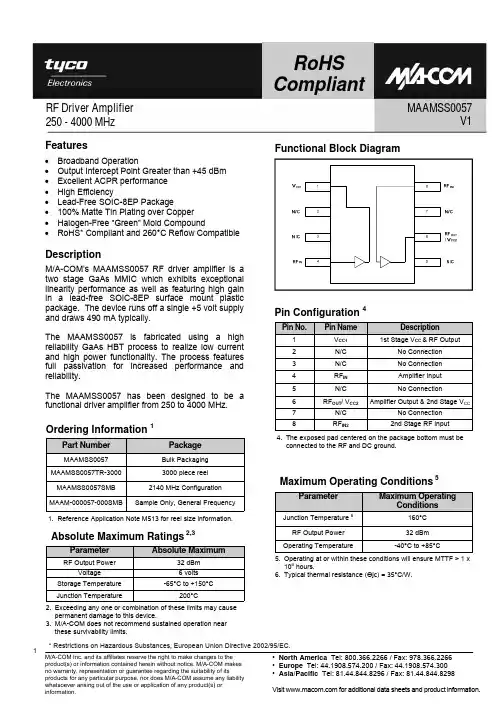
RF Driver Amplifier 250 - 4000 MHzMAAMSS0057V1CompliantFeatures• Broadband Operation• Output Intercept Point Greater than +45 dBm • Excellent ACPR performance • High Efficiency• Lead-Free SOIC-8EP Package• 100% Matte Tin Plating over Copper • Halogen-Free “Green” Mold Compound• RoHS* Compliant and 260°C Reflow CompatibleDescriptionM/A-COM’s MAAMSS0057 RF driver amplifier is a two stage GaAs MMIC which exhibits exceptional linearity performance as well as featuring high gain in a lead-free SOIC-8EP surface mount plastic package. The device runs off a single +5 volt supply and draws 490 mA typically.The MAAMSS0057 is fabricated using a high reliability GaAs HBT process to realize low current and high power functionality. The process features full passivation for increased performance and reliability.The MAAMSS0057 has been designed to be a functional driver amplifier from 250 to 4000 MHz.Ordering Information 1Part NumberPackageMAAMSS0057 Bulk Packaging MAAMSS0057TR-3000 3000 piece reel MAAMSS0057SMB 2140 MHz Configuration MAAM-000057-000SMBSample Only, General Frequency1. Reference Application Note M513 for reel size information.Pin Configuration 4Pin No.Pin NameDescription1 V CC1 1st Stage V CC & RF Output2 N/C No Connection3 N/C No Connection4 RF IN Amplifier Input5 N/C No Connection6 RF OUT / V CC2Amplifier Output & 2nd Stage V CC7 N/C No Connection 8RF IN22nd Stage RF InputFunctional Block DiagramAbsolute Maximum Ratings 2,3ParameterAbsolute MaximumRF Output Power32 dBmVoltage 6 volts Storage Temperature -65°C to +150°C Junction Temperature200°C2. Exceeding any one or combination of these limits may cause permanent damage to this device.3. M/A-COM does not recommend sustained operation near these survivability limits. Maximum Operating Conditions 5ParameterMaximum OperatingConditionsJunction Temperature 6 160°C RF Output Power 32 dBm Operating Temperature-40°C to +85°C5. Operating at or within these conditions will ensure MTTF > 1 x 10⁶ hours.6. Typical thermal resistance (Өjc) = 35°C/W.4. The exposed pad centered on the package bottom must be connected to the RF and DC ground.RF Driver Amplifier 250 - 4000 MHzMAAMSS0057V1 CompliantElectrical Specifications: T A = 25°C, Z0 = 50 Ω, V CC = 5VParameter Test Conditions Units Min. Typ. Max.Gain 2140 MHz dB 19 21 — Input Return Loss 2140 MHz dB — -10 — Output Return Loss 2140 MHz dB — -8 — Output P1dB 2140 MHz dBm — 31 —Output IP3 (+22 dBm / tone, 1 MHz spacing)2140 MHzdBm 42 45 —Channel Power (@ -45 dBc ACPR, WCDMA 64 channels fwd)2140 MHzdBm — 24 —Noise Figure 2140 MHz dB — 4.5 — Quiescent Current +5V mA — 490 —Current @ 22 dBm Output (+22 dBm / tone, 1 MHz spacing)2140 MHzmA — 600 750†† Reference Application Note M538 for lead-free solder reflow recommendations.RF Driver Amplifier 250 - 4000 MHzMAAMSS0057V1Compliant2140 MHz Schematic2140 MHz PCB LayoutParts ListPart Value Case StyleManufacturerPurpose C11000 pF 0402 Murata DC Block C21.5 pF 0402 MurataInput TuningC31000 pF 0402MurataBypassC4 0.1 μF0402 Murata BypassC5 1.5 pF 0402 Murata Inter-stage TuningC6 0.1 μF 0402 Murata Bypass C71000 pF 0402Murata BypassC8 1000 pF 0402Murata Output Tuning C91.2 pF 0402 Murata Inter-stage Tuning C10 1.2 pF 0402 Murata Inter-stage TuningC11 3.3 μF 1206 Murata Bypass L1 2.7 nH 0402 Coilcraft Input Tuning L2 7.5 nH 0402 Coilcraft Bias Injection L3 8.2 nH 0402 CoilcraftBias Injection J1 Jumper - - Jumper J2Jumper--JumperCross Section ViewThe PCB dielectric between RF traces and RF ground lay-ers should be chosen to reduce RF discontinuities between 50 Ω lines and package pins. M/A-COM recommends an FR-4 dielectric thickness of 0.008” (0.20 mm) yielding a 50 Ω line width of 0.015” (0.38 mm). The recommended RF metalization is 1 ounce copper. Handling ProceduresPlease observe the following precautions to avoid damage:Static SensitivityGallium Arsenide Integrated Circuits are sensitive to electrostatic discharge (ESD) and can be damaged by static electricity. Proper ESD control techniques should be used when handling these devices.RF Driver Amplifier 250 - 4000 MHzMAAMSS0057V1CompliantTypical Performance Curves: 2140 MHz Configuration over temperatureS11Output IP3GainS22Noise FigureP1dB10152025302.002.05 2.10 2.15 2.20 2.25+25°C+85°C -40°CFrequency (GHz)-35-30-25-20-15-10-502.002.05 2.10 2.15 2.20 2.25+25°C+85°C -40°CFrequency (GHz)10152025305101520253035+25°C+85°C -40°CPout (dBm)01234562.112.12 2.13 2.14 2.15 2.16 2.17+25°C-40°C +85°CFrequency (GHz)102030405060468101214161820222426OIP3L OIP3HOutput Power (dBm)/Tone-35-30-25-20-15-10-502.002.05 2.10 2.15 2.20 2.25+25°C+85°C -40°CFrequency (GHz)。
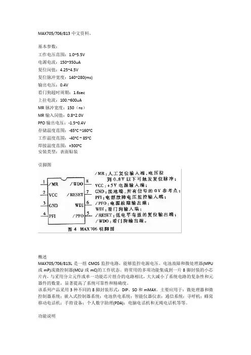
MAX705/706/813中文资料。
基本参数:工作电压范围:1.0~5.5V电源电流:150~350uA复位闵值:4.25~4.5V复位脉冲宽度:140~280(ms)输出电压:0.4V看门狗超时周期:1.6sec上拉电流:100.~600uAMR脉冲宽度:150(ns)MR输入闵值:0.8~2.0VPFO输出电压:-1.5~0.4V存储温度范围:-65°C ~160°C工作温度范围:-40°C ~ 85°C焊接温度范围:+300°C安装类型:表面贴装引脚图概述MAX705/706/813L是一组CMOS监控电路,能够监控电源电压、电池故障和微处理器(MPU 或mP)或微控制器(MCU或mC)的工作状态。
将常用的多项功能集成到一片8脚封装的小芯片内,与采用分立元件或单一功能芯片组合的电路相比,大大减小了系统电路的复杂性和元器件的数量,显著提高了系统可靠性和精确度。
该系列产品采用3种不同的8脚封装形式:DIP、SO和mMAX。
主要应用于:微处理器和微控制器系统;嵌入式控制器系统;电池供电系统;智能仪器仪表;通信系统;寻呼机;蜂窝移动电话机;手持设备;个人数字助理(PDA);电脑电话机和无绳电话机等等。
功能说明RESET/RESET操作复位信号用于启动或者重新启动MPU/MCU,令其进入或者返回到预知的循环程序并顺序执行。
一旦MPU/MCU处于未知状态,比如程序“跑飞”或进入死循环,就需要将系统复位。
对于MAX705和MAX706而言,在上电期间只要Vcc大于1.0V,就能保证输出电压不高于0.4V的低电平。
在Vcc上升期间RESET维持低电平直到电源电压升至复位门限(4.65V或4.40V)以上。
在超过此门限后,内部定时器大约再维持200ms后释放RESET,使其返回高电平。
无论何时只要电源电压降低到复位门限以下(即电源跌落),RESET引脚就会变低。
FEDL7050LA-021Semiconductor This version: June 2001Previous version: Sep. 2000 ML7050LABluetooth RF Transceiver ICGENERAL DESCRIPTIONThe Oki ML7050LA is a highly integrated Bluetooth TM radio transceiver designed to operate in the global 2.4 GHz Industrial, Scientific, and Medical (ISM) band. The ML7050LA architecture incorporates vital intermediate frequency (IF) and radio frequency (RF) circuits on a low cost, integration-friendly bulk CMOS process.Bluetooth technology directly supports short range, wireless voice and data communications with 1 Mbps throughput performance in the public ISM band across many applications, employing rapid frequency hopping (1.6K hops/s) spread spectrum (FHSS) approach. The ML7050LA highly integrated CMOS Bluetooth RF transceiver LSI will establish a 2.4 to 2.5 GHz communication link compliant with Bluetooth Specification Version 1.1 and is packaged in the Oki 48-pin ball grid array (BGA) package requires only 7 mm x 7 mm of the systems critical board space.Oki’s Bluetooth LSI family includes baseband LSI (ML70511LA), System Development Kit (BT-SDK), firmware and software (BTS Pack1/2/3). Together, the RF LSI (ML7050LA) and baseband (ML70511LA) devices form a complete hardware solution optimized for low system cost, small form factor, and reduced power consumption Bluetooth applications.FEATURES• Circuit design based on the Bluetooth Specification Version 1.1.• CMOS process technology lowers system cost and simplifies future baseband integration• Fully integrated CMOS RF LSI: TX/RX switch, power amplifier, LNA, image rejection mixer, VCO, PLL, gm-C IF filter, modulator, and demodulator.• Low IF circuitry eliminates off-chip SAW filter reducing bill-of-material (BOM)• Class 2 power operation compliant covering a wide range of applications• Seamless interface with Oki’s ML70511LA Bluetooth baseband controller LSI• Power supply voltage: 2.7 to 3.3 V• Package: 48-pin BGA (7 mm x 7 mm x 1.41mm)BLUETOOTH is a trademark owned by Bluetooth SIG, Inc. and licensed to Oki Electric Industry.The information contained herein can change without notice owing to the product being under development.1Oki SemiconductorML7050LABLOCK DIAGRAMABSOLUTE MAXIMUM RATINGSParameterSymbol Conditions Rating Unit Power supply voltage V DD Ta = 25°C–0.3 to 4.5V Input voltageV I –0.3 to V DD +0.3V Allowable power dissipation P D -0.5W Storage temperature T STG-–55 to +150°C In-Band TBD dBm Input RF Power-Out-of-Band TBDdBmRECOMMENDED OPERATING CONDITIONSParameterSymbol ConditionsMin.Typ.Max.Unit Power supply voltage V DD - 2.7 3.0 3.3VFull specification range Ta -0-55Operating temperature rangeTa-–20-+85°CPLL_CLK PLL_DATA PLL_LE PLL_OFFTXDRXDRF_AntTX_POW RX_POW PLL_POW LPF_CLIM_C2Tune_CVdd_PA Vdd_VCO Vdd_PLL Vdd_IFVdd_IRMLIM_C11Oki Semiconductor ML7050LA ELECTRICAL CHARACTERISTICS(VDD= 3.0V, Ta = 0 to +55°C) Symbol Description Conditions Min.Typ.Max.Unit Digital InputsVih Digital input high 2.4VDD+0.3V Vil Digital input low-0.30.4VDigital OutputsVoh Digital output high Ioh=-2mA 2.2 3.6VVol Digital output low Iol=2mA00.8VClockMCLK Master clock frequency-12.13,16-MHz Current Consumption Ta=25°CReceive Mode-55-mATransmit Mode-34-mA IDDOPLL Mode TX and RX disabled-22-mA IDDS Standby Mode V DD applied and powercontrol pins disabled-10-uA ReceiverF RF RF Frequency 2.4 2.5GHzR IN Reception sensitivity Includes ANT BPF loss,Note 1–75dBm -Maximum Received Signal–20dBm30 MHz to 1 GHz–57dBm-Spurious level1 GHz to 12.75 GHz–47dBm-Input VSWR-2:1-ZINRF Input impedance SW in50ΩTransmitterf RF RF Frequency 2.4 2.5GHzPO RF Output power fRF= 2.4 to 2.5 GHz,024dBm—Carrier frequency tolerance initial accuracy (static)-7575KHz f stab1Frequency drift(1 slot packet)-2525KHz f stab2Frequency drift(3 slot packet)-4040KHz f stab3Frequency drift(5 slot packet)-4040KHzMaximum frequency driftrate400Hz/µs —Power stability over temp TBD dBm —Modulation index0.280.35-±500 kHz–20dBmOffset = 2 MHz–20dBm —In-band spurious levelOffset > 3 MHz–40dBm1Oki Semiconductor ML7050LA30 MHz to 1 GHz–36dBm1 GHz to 12.75 GHz–30dBm—Out-of-band spurious level1.8 GHz to 1.9 GHz–47dBm5.15 GHz to 5.3 GHz–47dBm—Output VSWR-2:1-RF Output impedance SW out50ΩZOUTPLL@550 kHz–103dBc/Hz —Phase noise@2 MHz–120dBc/Hz —PLL lock-up time--150µs1Oki Semiconductor ML7050LAPIN LAYOUT (TOP VIEW)A1 ballcornerTOP VIEW1Oki Semiconductor ML7050LAPIN DESCRIPTIONPins for RF FunctionNo.Pin Name I/O DescriptionB1RF_Ant I/O RF connection to external BPF (antenna filter)D8Tune_C I Gm-C tuning components - Connect capacitors and resister between D8 and GNDC7 C8Lim_C1Lim_C2I Limiting amplifier capacitors - Connect capacitors between pins and GNDF8LPF_C I Low pass filter (LPF) capacitor - Connect capacitor between F8 and GNDG1 H1PLL_LF1PLL_LF2—External components for loop filter tuning:PLL_LF1 - Connect to VCOPLL_LF2 - Connect to PLLPins for TEST Interface, etc.G4MCLK I Master clock (12MHz, 13MHz or 16MHz) - CMOS level B7Test1I/OB8Test2I/OA5Test3IA6Test4ITest pins - Connect to GNDF1Test5O No connect - OpenE8Test6O No connect - OpenD2 E2Test7Test8O Test pins - Connect to GNDG6Test9O No connect - OpenH8Test10I/O No connect - OpenPins for Power Supply and GroundH6V dd_D—Power supply (V DD)- Digital; 3.0V+/-0.3V (from regulated voltage source) G7GND_D—Common Ground - DigitalD1V dd_PAE1V dd_VCOA2V dd_LNAH2V dd_PLLA3V dd_IRMA4V dd_IRM_LO E7, H7V dd_IF —Power supply (V DD) - Analog; 3.0V+/-0.3V(from regulated voltage source)A1/B2B4/B5C1/C2D7/F2F7/G2G5GND—Common ground (GND) - Analog1Oki Semiconductor ML7050LAPins for the Interface Between the RF LSI and the Baseband LSINo.Pin Name I/O DescriptionA8TXD I Transmit (TX) data - CMOS levelH5RXD O Receive (RX) data - CMOS levelH3PLL_DATA I PLL setup data: 6 Mbps <= PLL DATA <= 10 MbpsG3PLL_CLK I PLL clock setup: 6 MHz <= PLL CLK <= 10 MHzH4PLL_LE I PLL load enable setup: Data latched : ‘High’100 nsec <= PLL LEG8PLL_OFF I PLL Open-loop/Closed-loop mode control: Closed loop mode (receive): ‘High’Open loop mode (transmit) : ‘Low’A7PLL_POW I PLL power supply control switch: PLL Power ON : ‘Low’PLL Power OFF :’ High’B6TX_POW I Transmitter (TX) power supply control switch: TX ON (transmit) : ‘Low ‘TX OFF(receive) : ‘High’B3RX_POW I Receiver (RX) power supply control switch: RX ON (receive) : ‘Low’RX OFF (transmit) : ‘High’Modes of OperationBy setting or transitioning control pins, the device will enter into various modes of operation including receive, transmit, and standby.Mode Receive Transmit PLL StandbyPLL_POW0001TX_POW1011RX_POW01111Oki SemiconductorML7050LAPIN CONNECTION DIAGRAMThe externally connected components shown are tentative (April 2001).The ML7050LA provides a low bill-of-material (BOM) Bluetooth solution by minimizing external components. The design incorporates numerous internal tuning circuits using Gm-C and other leading-edge technologies to reliably control phase lock loop (PLL), VCO, amplifiers, modulator, and demodulator circuits. The TX-POW, RX_POW,PLL_POW, PLL-CLK, PLL_DATA, PLL_LE, PLL_OFF, RXD, and TXD connect directly to the complementary Bluetooth baseband (ML70511LA) device.PLL_CLK PLL_DATA PLL_LE PLL_OFF TXDRXDTX_POW RX_POW PLL_POW µF * The circuit is subject to change according to the specific board design. Please contact Oki Electric Industry Co., Ltd. for detailed information.1Oki Semiconductor ML7050LADESCRIPTION OF INTERNAL BLOCKS• Transmit filter (Gaussian filter):The input data is converted into a frequency modulation signal by a filter with Gaussian characteristics and is sent to the VCO.• Frequency control section (VCO, PLL, Loop Filter, AMP and SW):Generates a frequency in the 2.4 GHz to 2.5 GHz band (ISM band). During transmission, the VCO oscillator frequency is modulated by the modulation signal output by the Gaussian filter. The PLL frequency is controlled by the signals PLL_DATA, PLL_CLK, and PLL_LE. The switch SW (for Local) distributes the oscillator output to the transmitter circuit and the receiver circuit depending on the control signal (TX_POW/RX_POW).• Power amplifier (PA):This is the power amplifier for the transmitter.• Transmit/Receive selection switch (SW for Ant)Depending on the control signal (TX_POW/RX_POW), this switch feeds the output of the power amplifier to the antenna during transmission. During reception, the received signal of the antenna is fed to the LNA.• Reception amplifier (LNA):This amplifies the weak RF received signal from the antenna.• Image Rejection Mixer (IRM):Converts the output signal from the LNA (2.4 to 2.5 GHz) into an intermediate frequency and also eliminates the image frequency component.• IF Band pass filter (IF BPF):Removes the signal of the nearby bands.• Limiting amplifier:Amplifies the signal converted into the intermediate frequency up to a specific amplitude.• Demodulator (DEMOD):The received signal is demodulated using the delay detector circuit.• Filter tuning (Gm-C Tuning):The reference clock is compared with the oscillator frequency inside the tuning circuit, and the frequency characteristics of the Gm-C filter is adjusted automatically.1Oki Semiconductor ML7050LA PLL METHODOLOGY1Oki SemiconductorML7050LAPLL Computation MethodFvcoFosc (0 <= A<=31)MxN+AR(M × N + A denotes (M - A) × 32 + A × 33)R:Reference counter set value N:Programmable counter set value A:Swallow counter set valuePLL Reference CounterFreq R R(Bin)(MHz)(Dec)R4R3R2R1R055001016600110770011188010009901001101001010111101011121201100131301101141401110151501111161610000171710001181810010191910011202011Programmable Counter and Swallow CounterF.step 1 MHz M32 div(RX PLL Frequency) = (TX PLL Frequency) – 2MHz* In receive mode, PLL generates local frequency for IRM. Intermediate frequency is 2MHz.N(Bin)A(Bin)Freq.(MHz)N (Dec)A (Dec)N6N5N4N3N2N1N0A4A3A2A1A023977429100101011101239874301001010111102399743110010101111124007501001011000002401751101110011Oki Semiconductor ML7050LA2402752100101100010:::::::::::::::::::::::::::::::::::::::::::::249678010011100000024977811001110000012498782100111000010249978310011100001125007841001110001001Oki SemiconductorML7050LAPLL Set-up Time ChartR4 to R0:Binary 5-bit reference counter (5-20)N6 to N0:Programmable counter (7 bits)See "PLL Setting method”.A4 to A0:Swallow counter (0-31) (5 bits)See "PLL Setting method”.CTL:When CTL is "H", the input data is handed over to the reference counter register.When CTL is "L", the input data is handed over to the programmable and swallow counter register.Note: Start data input from the MSB.123456789101112131415161718192021222324252627282930313233343536373839404142123456789101112131415161718192021CLK DATAMSBLSBLE1Oki SemiconductorML7050LASYSTEM OVERVIEWTogether, RF (ML7050LA) and baseband (ML70511LA) devices form a complete hardware solution optimized for low system cost, small form factor, and reduced power consumption wireless applications. The ML70511LA baseband IC controls the ML7050LA frequency selection, tuning characteristics, and control functions through writing to internal registers. ML7050LA can then read-back the register information to ML70511LA insuring proper modes of operation. The communication between the devices occurs on Oki’s proprietary, low pin count serial interface. The connection between a host controller or processor and the baseband device is implemented via USB (version 1.1) or UART.Power SupplyThe analog power supply (V DD ) voltage is connected to pins serving each analog functional blocks (Vdd_PA,Vdd_LNA, Vdd_VCO, Vdd_PLL, Vdd_IF, Vdd_IRM and Vdd_IRM_LO). A separate digital power supply voltage is required by the digital section. Each of the analog power supply voltage should be supplied from regulated voltage source and should be low-frequency de-coupled by external blocking capacitors.GroundIn order to minimize electrical noise and other interference, the ground plane should be distributed with low impedance characteristics including underneath the ML7050LA. Connect all GND pins to the ground plane.1Oki Semiconductor ML7050LA PACKAGE DIMENSIONS (48-PIN BGA)(Unit: mm)1Oki Semiconductor ML7050LA NOTICE1.The information contained herein can change without notice owing to product and/or technical improvements.Before using the product, please make sure that the information being referred to is up-to-date.2.The outline of action and examples for application circuits described herein have been chosen as an explanationfor the standard action and performance of the product. When planning to use the product, please ensure that the external conditions are reflected in the actual circuit, assembly, and program designs.3.When designing your product, please use our product below the specified maximum ratings and within thespecified operating ranges including, but not limited to, operating voltage, power dissipation, and operating temperature.4.Oki assumes no responsibility or liability whatsoever for any failure or unusual or unexpected operation resultingfrom misuse, neglect, improper installation, repair, alteration or accident, improper handling, or unusual physical or electrical stress including, but not limited to, exposure to parameters beyond the specified maximum ratings or operation outside the specified operating range.5.Neither indemnity against nor license of a third party’s industrial and intellectual property right, etc. is granted byus in connection with the use of the product and/or the information and drawings contained herein. No responsibility is assumed by us for any infringement of a third party’s right which may result from the use thereof.6.The products listed in this document are intended for use in general electronics equipment for commercialapplications (e.g., office automation, communication equipment, measurement equipment, consumer electronics, etc.). These products are not authorized for use in any system or application that requires special or enhanced quality and reliability characteristics nor in any system or application where the failure of such system or application may result in the loss or damage of property, or death or injury to humans.Such applications include, but are not limited to, traffic and automotive equipment, safety devices, aerospace equipment, nuclear power control, medical equipment, and life-support systems.7.Certain products in this document may need government approval before they can be exported to particularcountries. The purchaser assumes the responsibility of determining the legality of export of these products and will take appropriate and necessary steps at their own expense for these.8.No part of the contents contained herein may be reprinted or reproduced without our prior permission.Copyright 2001 Oki Electric Industry Co., Ltd.。
7805中文资料/LM7805中文资料LM7805是常用的三端稳压器,一般使用的是TO-220封装,能提供DC 5V的输出电压,应用范围广,内含过流和过载保护电路。
带散热片时能持续提供1A的电流,如果使用外围器件,它还能提供不通的电压和电流。
LM7805引脚图(管脚图)7805是常用的三端稳压器件,顾名思义05就是输出电压为5v,还可以微调,7805输出波纹很小。
(1) 集成三端稳压器根据稳定电压的正、负极性分为78×××,79×××系列。
附图给出了正、负稳压的典型电路。
〈正、负稳压7805电路〉(2) 三端稳压器的型号规格和管脚分布。
例如:78M05三端稳压器可输出+5 V、A的稳定电压;7912三端稳压器可输出12V、1A的稳定电压。
(3) 外形及管脚分布,如附图1-25所示。
由7805,7905,7812组成的特殊的线性稳压电源如图所示为一种特殊的电源电路。
该电路虽然简单,但可以从两个相同的次级绕组中产生出三组直流电压:+5V、-5V和+12V。
其特点是:D2、D3跨接在E2、E3这两组交流电源之间,起着全波整流的作用。
78057805三端稳压集成电路,电子产品中,常见的三端稳压集成电路有正电压输出的78 ×× 系列和负电压输出的79××系列。
顾名思义,三端IC是指这种稳压用的集成电路,只有三条引脚输出,分别是输入端、接地端和输出端。
它的样子象是普通的三极管,TO- 220 的标准封装,也有9013样子的TO-92封装。
基本信息中文名称7805三端稳压集成电路最大输出电流特点热过载保护、短路保护、使用方便输入电压不大于36V输入输出压差2V输出电压~结构组成用78/79系列三端稳压IC来组成稳压电源所需的外围元件极少,7805三端稳压集成电路电路内部还有过流、过热及调整管的保护电路,使用起来可靠、方便,而且价格便宜。
•Rugged electrical and mechanical design •Outputs individually controlled with excellent dynamic properties•Operating ambient temperature range –40...71°CWide input voltage from 8...372 V DC1, 2 or 3 isolated outputs up to 48 V DC 4 kV AC I/O electric strength test voltageSelection chartLGACM, DM and LM types available as CMZ, DMZ and LMZ class II equipment2/12.2000Input voltage 6 wide-input ranges (1:5)refer to selection chartOutputEfficiency U i nom, I o nom up to 83%i nom o nom±0.6% U o nom Output voltage switching noise IEC/EN 61204, total typ. 50 mV ppi min i max o nom o nom Load regulation U i nom, 0...I o nom, each output regulated typ. 0.15% U o nom Minimum load not required0 A Current limitation main output rectangular U/I characteristic typ. 110% I o nomo nom Operation in parallel by current limitation, only main outputsi nom o nomU i nom, I o nom, A/B/C/D/FM with ext. diode in input line up to 7 msProtectionInput reverse polarity built-in fusei min Input overvoltage lockout typ. 110% U i maxOutput no-load, overload and short circuit proofo nom Overtemperature switch-off with auto restart T C typ. 100°CControlOutput voltage adjustment single output types0...110% U o nom Status indication LEDs: OK, inhibit, overloadSafetyApprovals EN 60950, UL 1950, CSA C22.2 No. 950Class of equipment AM, BM, CM, DM, FM, LM class I Protection degree units without options IP 40class I, I/O 4 kV ACO/case 1 kV ACElectrostatic discharge IEC/EN 61000-4-2, level 4 (8/15 kV)criterion B Electromagnetic field IEC/EN 61000-4-3, level x (20 V/m)criterion A/B Electr. fast transients/bursts IEC/EN 61000-4-4, input, level 3/4 (2/4 kV)criterion A/B Surge IEC/EN 61000-4-5, input, level 3/4 (2/4 kV)criterion A Electromagnetic emissions CISPR 22/EN 55022, conducted class BEnvironmentalOperating ambient temperature U i nom, I o nom, convection cooled–25...71°C Operating case temperature C i nom, o nom–25...95°C Storage temperature non operational–40...100°C Damp heat IEC/EN 60068-2-3, 93%, 40°C56 daysn Shock IEC/EN 60068-2-27, 6 ms100 g nn Random vibration IEC/EN 60068-2-64, 20...500 Hz 4.9 g n rms MTBF MIL-HDBK-217E, G B, 40°C, single output types320'000 h OptionsExtended temperature range–40...71°C, ambient, operating-9 Electronic inrush current limitation Eo nomInput and/or output undervoltage monitoring, excludes option V D0...D9 Test sockets for check of output voltage A Enhanced electric strength test 2 kV AC H Fuse not user accessible FPin allocationMechanical data ArrayTolerances ±0.3 mm (0.012") unless otherwise indicated.AccessoriesFront panels 19” (Schroff/Intermas)Mating H11 connectors with screw, solder, fast-on or press-fit terminalsConnector retention facilities and code key system for connector codingFlexible PCB for connecting the converter via an H11 connector, if mounted on a PCB Chassis or wall mounting plates for frontal accessUniversal mounting brackets for chassis or DIN-rail mounting。
SLA7052M中文资料Data Sheet28210.1B* UNIPOLAR STEPPER-MOTOR TRANSLATOR/PWM DRIVERCombining low-power CMOS logic with high-current, high-voltagepower FET outputs, the SLA7052M translator/driver provides completecontrol and drive for a two-phase unipolar stepper motor with internalfixed off time, pulse-width modulation (PWM) control of the outputcurrent in a power multi-chip module (PMCM?).The CMOS logic section provides the sequencing logic, direction,full/half-step control, synchronous/asynchronous PWM operation, anda “sleep” function. The minimum CLOCK input is an idealapplications where a complex μP is unavailable or overburdened. TTLor LSTTL may require the use of appropriate pull-up resistors to ensurea proper input-logic high. For PWM current control, the maximumoutput current is determined by the user’s selection of a referencevoltage and sensing resistor. The NMOS outputs are capable of sinkingup to 3 A and withstanding 46 V in the off state. Ground-clamp andflyback diodes provide protection against inductive transients. Specialpower-up sequencing is not required.Full-step (2 phase) and half-step operation are externally selectable.Two-phase drive energizes two adjacent phases in each detent position(AB-BC-CD-DA). This sequence mode offers an improved torque-speed product, greater detent torque, and is less susceptable to motorresonance. Half-step excitation alternates between the one-phase andtwo-phase modes (A-AB-B-BC-C-CD D-DA), providing an eight-stepsequence.The SLA7052M is supplied in an 18-pin single in-line power-package with leads formed for vertical mounting (suffix LF871) orhorizontal mounting (suffix LF872). The tab is at ground potential andneeds no insulation. For high-current or high-frequency applications,external heat sinking may be required. This device is rated for continu-ous operation between -20°C and +85°C.F EATURES3 A Output RatingInternal Sequencer for Full or Half-Step OperationPWM Constant-Current Motor DriveCost-Effective, Multi-Chip Solution100 V, Avalanche-Rated NMOSLow r DS(on) NMOS Outputs (150 m? typical)Advanced, Improved Body DiodesHalf-Step and Full-Step Unipolar DriveInputs Compatible with 3.3 V or 5 V Control SignalsSleep ModeInternal Clamp DiodesAlways order by complete part number, e.g., SLA7052MLF871 .A BSOLUTE M AXIMUM R ATINGSDriver Supply Voltage, V BB.................46 VLoad Supply Voltage, V M...................46 VOutput Current, I O............................3.0 A*Logic Supply Voltage, V DD................7.0 VLogic Input Voltage Range,V I........................... -0.3 V to V DD+ 0.3 VSense Voltage, V S........................±2.0 V?Reference Input Voltage Range,V REF...................................-0.3 V to V DD+ 0.3 V Package Power Dissipation,P D........................................See GraphJunction Temperature, T J.............+150°COperating Temperature Range,T A.................................-20°C to +85°CStorage Temperature Range,T S...............................-30°C to +150°C* Output current rating may be limited by duty cycle, ambient temperature, and heat sinking. Under any set of conditions, do not exceed the specified current rating or junction temperature.Internal filtering provides protection against transients during the first 1 μs of the current-sense pulse.SLA7052MMo t orD ri v erSanken Power Devicesfrom Allegro MicroSystemsSLA7052MUNIPOLAR STEPPER-MOTOR TRANSLATOR/PWM DRIVER2M o t o r Dr i v e r Functional block diagramRecommended operating conditionsLoad Supply Voltage, V BB .................................. 10 to 44 V Logic Supply Voltage, V DD ............................ 3.0 V to 5.5 V Reference Input Voltage, V REF ...................... 0.1 V to 1.0 V Tab Temperature (no heat sink), T T ...................... <100°CSLA7052MUNIPOLAR STEPPER-MOTOR TRANSLATOR/PWM DRIVER3M o t o r Dr i v e r Electrical characteristics: unless otherwise noted at T A = +25°C, V BB = 24 V, V DD = 5.0 V.LimitsCharacteristic SymbolTest ConditionsMin.Typ.Max.UnitsOutput driversDriver Supply Volt. Range V BB Operating10—44V Drain-Source Breakdown V (BR)DS V BB = 44 V, I D = 1 mA 100——V Output On Resistance r DS(on)I O = 3.0 A —150270m ?Body Diode Forward Volt.V F I F = 3.0 A— 1.5 2.3V Driver Supply CurrentI BB——15mA V REF > 2.0 V (sleep mode)——100μAControl logicLogic Supply Volt. Range V DD Operating3.0 5.0 5.5V Logic Input VoltageV IH 0.75V DD——V V IL——0.25V DDV Logic Input CurrentI IH —±1.0—μA I IL—±1.0—μA Max. Clock Frequency f clk 100*——kHz PWM Off Time t off —12—μs PWM Min. On Time t on(min)— 5.0—μs Ref. Input Voltage RangeV REFOperating 0.0— 1.5V Sleep mode2.0——V Ref. Input Current I REF —±10—μA Sense VoltageV S Trip point—V REF —V Propagation Delay Timet PLH Clock rising edge to output on — 2.5—μs t PHLClock rising edge to output off —2.0—μs Logic Supply CurrentI DD——3.0mATypical values are given for circuit design information only.*Operation at a clock frequency greater than the specified minimum value is possible but not warranted.SLA7052MUNIPOLAR STEPPER-MOTOR TRANSLATOR/PWM DRIVER4M o t o r Dr i v e r Timing chartLogic input timingSLA7052MUNIPOLAR STEPPER-MOTOR TRANSLATOR/PWM DRIVER5M o t o r Dr i v e r Functional descriptionDevice operation. The SLA7052M is a complete stepper-motor driver with built-in translator for easy operation with minimal control lines. It is designed to operate unipolar stepper motors in full-step or half-step modes. The current in each pair of outputs, all n-channel MOSFETs, is regulated with internal fixed off-time pulse-width modulated (PWM) control circuitry.When a step command signal occurs on the clock input the translator automatically sequences to the next step.Clock (step) input. A low-to-high transition on the clock input sequences thetranslator and advances the motor one increment. The hold state is done by stopping the CLOCK input regardless of the input level Full/half-step select. This logic-level input sets the translator step mode. A logic low is two-phase, full step; a logic high is half step. Changes to this input do not take effect until the rising edge of the clock input.CW/CCW (direction) input. This logic-level input sets the translator step direction. Changes to this input do not take effect until the rising edge of the clock input.Internal PWM current control. Each pair of outputs is controlled by a fixed off-time PWM current-control circuit that limits the load current to a desired value (I TRIP ).Initially, an output is enabled and current flows through the motor winding and R S . When the voltage across the current-sense resistor equals the reference voltage, the current-sense comparator resets the PWM latch, which turns off the driver for the fixed off time during which the load inductance causes the current to recirculate for the off time period. The driver is then re-enabled and the cycle repeats.Synchronous operation mode. This function pre-vents occasional motor noise during a “hold” state, which normally results from asynchronous PWM operation of both motor phases.A logic high at the SYNC input is synchronous operation; a logic low is asynchronous operation. The use of synchronous operation during normal stepping is not recommended because it produces less motor torque and can cause motor vibration due to stair-case current.Sleep mode. Applying a voltage greater than 2 V to the REF pin disables the outputs and puts the motor in a free state (coast). This function is used to minimize power consumption when notin use. It disables much of the internal circuitry including the output MOSFETs and regulator. When coming out of sleep mode, wa it 100 μs before issuing a step command to allow the internal circuitry to stabilize.SLA7052MUNIPOLAR STEPPER-MOTOR TRANSLATOR/PWM DRIVER6Mo t orD ri v erApplications informationLayout.The printed wirting board should use a heavy groundplane.For optimum electrical and thermal performance, thedriver should be soldered directly into the board.The driver supply terminal, VBB, should be decoupledwith an electrolytic capacitor placed as close to the device as possible.To avoid problems due to capacitive coupling of thehigh dv/dt switching transients, route the high-level, output traces away from the sensitive, low-level logic traces. Always drive the logic inputs with a low source impedance to increase noise immunity.Grounding. A star ground system located close to the driver is recommended. The logic supply return and the driver supply return should be connected together at only a single point — the star ground.Logic supply voltage, VDD. Transients at this terminalshould be held to less than 0.5 V to avoid malfunctioning operation. Both VBBand VDDmay be turned on or offseparately.Logic inputs. Unused logic inputs (CW/CCW, FULL/ HALF, or SYNC) must be connected to either ground orthe logic supply voltage.Current sensing. T o minimize inaccuracies caused by ground-trace IR drops in sensing the output current level, the current-sense resistor, RS, should have an independentground return to the star ground of the device. This path should be as short as possible. For low-value sense resistors, the IR drops in the printed wiring board sense resistor’s traces can be significant and should be taken into account. The use of sockets should be avoided as they can introduce variation in RSdue to their contact resistance.PWM current control. The maximum value of current limiting (ITRIP) is set by the selection of RSand the voltageat the REF input with a transconductance function ap- proximated by:ITRIP= VREF/RSThe required VREFshould not be less than 0.1 V. If it is,RSshould be increased for a proportionate increase inVREF.Typical applicationSLA7052MUNIPOLAR STEPPER-MOTOR TRANSLATOR/PWM DRIVER7M o t o r Dr i v e r Applications Information (cont’d)Continuous Discontinuous mode modeNormalized FET on resistanceSync. signal generatorReference voltage. In the Typical Application shown,resistors R 1 and R 2 set the reference voltage as:V REF = (V DD x R 2)/(R 1 + R 2)The trimming of R 2 allows for the resistor tolerances and REF input current. The sum of R 1+R 2 should be less than 50 k ? to minimize the effect of I REF .Minimum output current. The SLA7052M uses fixed off-time PWM current control. Due to internal logic and switching delays, the actual load current peak will be slightly higher than the calculated I TRIP value (especially for low-inductance loads). These delays, plus the mini-mum recommended V REF , limit the minimum value the current-control circuitry can regulate. An application with this device should maintain continuous PWM control in order to obtain optimum torque out of the motor. The boundary of the load current (I O(min)) between continuous and discontinuous operation is:I O(min) = [(V M + V SD )/R m ] x [(1/e t off /[R m x L m ]) -1]where V M = load supply voltageV F = body diode forward voltage R m = motor winding resistance t off = PWM off timeL m = motor winding inductanceTo produce zero current in a motor, the REF input should be pulled above 2 V, turning off all drivers.Synchronous operation mode. If an external signal is not available to control the synchronous operationmode, a simple circuit can keep the SYNC input low while the CLOCK input is active; the SYNC input will go high (synchronous operation) when the CLOCK input stays low (“hold”). The RC time constant determines the sync trransition timing.Temperature effects on FET outputs. Analyzing safe, reliable operation includes a concern for the relation-ship of NMOS on resistance to junction temperature.Device package power calculations must include the increase in on resistance (producing higher on voltages)caused by increased operating junction temperatures. The figure provides a normalized on-resistance curve, and allthermal calculations should consider increases from theSLA7052MUNIPOLAR STEPPER-MOTOR TRANSLATOR/PWM DRIVER8M o t o r Dr i v e r Applications Information (cont’d)Allowable avalanche energyWaveforms during avalanche breakdowngiven +25°C limits, which may be caused by internal heating during normal operation.These power MOSFET outputs feature an excellentcombination of fast switching, ruggedized device design,low on resistance, and cost effectiveness.Avalanche energy capability. There is a surge voltage expected when the output MOSFET turns off, and this voltage may exceed the MOSFET breakdown voltage (V (BR)DS ). However, the MOSFETs are avalanche type and as long as the energy (E (AV)), which is imposed on the MOSFET by the surge voltage, is less than the maximum allowable value, it is considered to be within its safe operating area. Note that the maximum allowable ava-lanche energy is reduced as a function of temperature.In application, the avalanche energy (E (AV)) dissipated by the MOSFET is approximated asE (AV) = V DS(AV) x 1/2 x I D x tOutput circuit for avalanche energycalculationsSLA7052MUNIPOLAR STEPPER-MOTOR TRANSLATOR/PWM DRIVER9M o t o r Dr i v e r Terminal listTerminal Pin Name Terminal Description 1OUT A Driver output for phase A 2NU Not usable3OUT A \Driver output for phase A\4GATE A Phase AMOSFET Gate 5V DD Logic power supply 6SENSE A Phase A current sense 7CLOCK Step clock input8SYNC Synchronous PWM control input 9REF Current set & “sleep” control 10GND Supply negative return11CW/CCWForward/reverse logic control input12FULL/HALF Full step/half step logic control input 13SENSE B Phase B current sense 14V BB Driver power supply 15GATE B Phase B MOSFET Gate 16OUT B \Driver output for phase B\17NU Not usable18OUT BDriver output for phase BThe products described herein are manufactured in Japan by Sanken Electric Co., Ltd. for sale by Allegro MicroSystems, Inc.Sanken and Allegro reserve the right to make, from time to time,such departures from the detail specifications as may be required to permit improvements in the performance, reliability, ormanufacturability of its products. Therefore, the user is cautioned to verify that the information in this publication is current before placing any order.When using the products described herein, the applicability and suitability of such products for the intended purpose shall be reviewed at the users responsibility.Although Sanken undertakes to enhance the quality and reliability of its products, the occurrence of failure and defect of semiconductor products at a certain rate is inevitable.Users of Sanken products are requested to take, at their own risk,preventative measures including safety design of theequipment or systems against any possible injury, death, fires or damages to society due to device failure or malfunction.Sanken products listed in this publication are designed and intended for use as components in general-purpose electronic equipment or apparatus (home appliances, office equipment, telecommunication equipment, measuring equipment, etc.). Their use in any application requiring radiation hardness assurance (e.g., aerospace equipment) is not supported.When considering the use of Sanken products in applications where higher reliability is required (transportation equipment and its control systems or equipment, fire- or burglar-alarm systems, various safety devices, etc.), contact a Sanken sales representative to discuss and obtain written confirmation of your specifications.The use of Sanken products without the written consent of Sanken in applications where extremely high reliability is required (aerospace equipment, nuclear power-control stations, life-support systems, etc.) is strictly prohibited.The information included herein is believed to be accurate and reliable. Application and operation examples described in this publication are given for reference only and Sanken and Allegro assume no responsibility for any infringement of industrial property rights, intellectual property rights, or any other rights of Sanken or Allegro or any third party that may result from its use.SLA7052MUNIPOLAR STEPPER-MOTOR TRANSLATOR/PWM DRIVER10M o t o r Dr i v e r NOTES: 1.Exact body and lead configuration at vendor’s option within limits shown.2.Lead spacing tolerance is non-cumulative.3.The shaded area is exposed heat spreader.3.Recommended mounting hardware torque: 0.490 - 0.822 Nm.4.Recommended use of metal-oxide-filled, alkyl-degenerated oil-base silicone grease: Dow Corning SC102,Toshiba YG6260, Shin-Etsu G746, or equivalent.SLA7052MLF871Dimensions in inches(for reference only)Dimensions in millimeters(controlling dimensions)SLA7052MUNIPOLAR STEPPER-MOTOR TRANSLATOR/PWM DRIVER11M o t o r Dr i v e r NOTES: 1.Exact body and lead configurati on at vendor’s option within limits shown.2.Lead spacing tolerance is non-cumulative.3.The shaded area is exposed heat spreader.3.Recommended mounting hardware torque: 0.490 - 0.822 Nm.4.Recommended use of metal-oxide-filled, alkyl-degenerated oil-base silicone grease: Dow Corning SC102,Toshiba YG6260, Shin-Etsu G746, or equivalent.SLA7052MLF872Dimensions in inches(for reference only)Dimensions in millimeters(controlling dimensions)SLA7052MUNIPOLAR STEPPER-MOTOR TRANSLATOR/PWM DRIVER 12M o t o r Dr i v e r Packing information20 sticks/tubes in Y direction;3 layers of sticks/tubes in Z direction = 1080 devices per box.18 devices per stick/tube.A rubber stopper is provided at each end of the stick/tube.。