Chemical bath deposited CdS CdSe-sensitized porous TiO2 solar cells
- 格式:pdf
- 大小:585.56 KB
- 文档页数:8

W B试剂各组分作用 Document number:NOCG-YUNOO-BUYTT-UU986-1986UT
acr和bis:当然是产生凝胶的最基本物质。
SDS:使蛋白在胶中可以保持变性
-Hcl:使分离胶的pH保持在,浓缩胶的pH保持在
对于浓缩胶来说,可以通过甘氨酸和和氯离子的作用产生压缩,从而使蛋白条带压细。
对于分离胶来说,与甘氨酸的pka接近,从而使不同分子量的蛋白产生不同的泳动速度,从而使不同分子量的蛋白分开。
TEMED和AP:这两种物质的作用都是催化剂。
样品处理液中加入适量的甘油或蔗糖,是为了增大溶液密度,使加样时样品溶液可以沉入样品加样槽底部.
sds作为阴离子去污剂,其作用应至少有三:
1.断裂分子内和分子间的氢键,使蛋白质分子去折叠,破坏蛋白质分子的二三级结构,消除蛋白质在迁移过程中结构的影响;
2.与蛋白质形成-蛋白质复合物,由于sds带有大量负电荷,好比蛋白质穿上带负电的“外衣”,蛋白质本身带有的电荷则被掩盖了,从而消除蛋白质在迁移过程中自身电荷的差异造成的影响。
那么蛋白质的迁移速度就只与其本身分子量的大小有关了(分子筛效应的作用)
3.可起到助溶作用,使结合了sds的蛋白质变为亲水性,易于在水相中迁移。
AP提供acr和bis聚合的氧自由基,是acr和bis聚合的引发剂,TEMED可催化AP释放氧自由基,是反应的催化剂。
![双脱水半乳糖醇和其衍生物或类似物的制剂的分析和分辨方法[发明专利]](https://img.taocdn.com/s1/m/b6c81df4c281e53a5902ff86.png)
专利名称:双脱水半乳糖醇和其衍生物或类似物的制剂的分析和分辨方法
专利类型:发明专利
发明人:徐强
申请号:CN201680076100.X
申请日:20161122
公开号:CN108699018A
公开日:
20181023
专利内容由知识产权出版社提供
摘要:一种用于分析双脱水半乳糖醇制剂的改进的分析方法,提供用于测定双脱水半乳糖醇的纯度并检测双脱水半乳糖醇制剂中的杂质以及鉴别任何此类杂质的方法。
所述方法采用高效液相色谱HPLC,尤其采用具有ELSD检测的逆相酰胺色谱柱的HPLC;所述HPLC可以接着串联质谱。
所述方法可另外包括进行双脱水半乳糖醇制剂中存在的至少一种特定物质峰的制备型HPLC采集的步骤。
申请人:德玛医药(BC)有限公司
地址:加拿大不列颠哥伦比亚省
国籍:CA
代理机构:北京律盟知识产权代理有限责任公司
代理人:陈甜甜
更多信息请下载全文后查看。

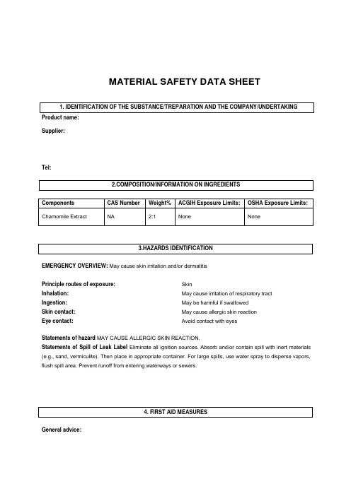
1. IDENTIFICATION OF THE SUBSTANCE/TREPARATION AND THE COMPANY/UNDERTAKING3.HAZARDS IDENTIFICATION4. FIRST AID MEASURESMATERIAL SAFETY DATA SHEETProduct name:Supplier:Tel:EMERGENCY OVERVIEW: May cause skin irritation and/or dermatitisPrinciple routes of exposure: Inhalation: Ingestion: Skin contact: Eye contact:SkinMay cause irritation of respiratory tract May be harmful if swallowed May cause allergic skin reaction Avoid contact with eyesStatements of hazard MAY CAUSE ALLERGIC SKIN REACTION.Statements of Spill of Leak Label Eliminate all ignition sources. Absorb and/or contain spill with inert materials (e.g., sand, vermiculite). Then place in appropriate container. For large spills, use water spray to disperse vapors, flush spill area. Prevent runoff from entering waterways or sewers.General advice:POSITION/INFORMATION ON INGREDIENTSInhalation:Skin contact:Ingestion:Eye contact:Protection of first – aiders:Medical conditions aggravated by exposure: In the case of accident or if you fell unwell, seek medical advice immediately (show the label where possible).Move to fresh air, call a physician immediately.Rinse immediately with plenty of water and seek medical adviceDo not induce vomiting without medical advice.In the case of contact with eyes, rinse immediately with plenty of water and seek medical advice.No information availableNone knownSuitable extinguishing media:Specific hazards:Special protective equipment for firefighters:Flash point:Autoignition temperature:NFPA rating Use dry chemical, CO2, water spray or “alcohol” foam Burning produces irritant fumes.As in any fire, wear self-contained breathing apparatus pressure-demand, MSHA/NIOSH (approved or equivalent) and full protective gearNot determinedNot determinedNFPA Health: 1 NFPA Flammability: 1 NFPA Reactivity: 0Personal precautions: Environmental precautions: Methods for cleaning up: Use personal protective equipment.Prevent product from entering drains.Sweep up and shovel into suitable containers for disposalStorage:7. HANDLING AND STORAGE5.FIRE-FIGHTING MEASURES6. ACCIDENTAL RELEASE MEASURESRoom temperature Handling:Safe handling advice: Incompatible products:Use only in area provided with appropriate exhaust ventilation.Wear personal protective equipment.Oxidising and spontaneously flammable productsEngineering measures: Respiratory protection: Skin and body protection:Eye protection: Hand protection: Hygiene measures:Ensure adequate ventilation.Breathing apparatus only if aerosol or dust is formed. Usual safety precautions while handling the product will provide adequate protection against this potential effect. Safety glasses with side-shieldsPVC or other plastic material glovesHandle in accordance with good industrial hygiene and safety practice.Melting point/range: Boiling point/range: Density: Vapor pressure: Evaporation rate: Vapor density: Solubility (in water): Flash point:Autoignition temperature:No Data available at this time. No Data available at this time. No data available No data available No data available No data available No data available Not determined Not determinedStability: Stable under recommended storage conditions. Polymerization: None under normal processing.Hazardous decomposition products: Thermal decomposition can lead to release of irritating gases and vapours such as carbon oxides.Materials to avoid: Strong oxidising agents.10. STABILITY AND REACTIVITY9. PHYSICAL AND CHEMICAL PROPERTIES8. EXPOSURE CONTROLS/PERSONAL PROTECTION11. TOXICOLOGICAL INFORMATIONConditions to avoid: Exposure to air or moisture over prolonged periods.Product information Acute toxicityChronic toxicity:Local effects: Chronic exposure may cause nausea and vomiting, higher exposure causes unconsciousness.Symptoms of overexposure may be headache, dizziness, tiredness, nausea and vomiting.Specific effects:May include moderate to severe erythema (redness) and moderate edema (raised skin), nausea, vomiting,headache.Primary irritation: Carcingenic effects: Mutagenic effects: Reproductive toxicity:No data is available on the product itself. No data is available on the product itself. No data is available on the product itself. No data is available on the product itself.Mobility:Bioaccumulation: Ecotoxicity effects: Aquatic toxicity:No data available No data available No data availableMay cause long-term adverse effects in the aquatic environment.12. ECOLOGICAL INFORMATION13. DISPOSAL CONSIDERATIONSWaste from residues/unused products:Contaminated packaging:Waste disposal must be in accordance with appropriate Federal, State and local regulations. This product, if unaltered by use, may be disposed of treatment at a permitted facility or as advised by your local hazardous waste regulatory authority. Residue from fires extinguished with this material may be hazardous.Do not re-use empty containers.UN/Id No:Not regulated14. TRANSPORT INFFORMATIONDOTProper shipping name: Not regulatedTGD(Canada)WHMIS hazard class: Non - controlledIMDG/IMOIMDG – Hazard Classifications Not ApplicableIMO – labels:15. REGULATORY INFOTMATION International Inventories16. OTHER INFORMATIONPrepared by: Health & SafetyDisclaimer: The information and recommendations contained herein are based upon tests believed to be reliable.However, XABC does not guarantee the accuracy or completeness NOR SHALL ANY OF THIS INFORMATION CONSTITUTE A WARRANTY, WHETHER EXPRESSED OR IMPLIED, AS TO THE SAFETY OF THE GOOD, THE MERCHANTABILITY OF THE GOODS, OR THE FITNESS OF THE FITNESS OF THE GOODS FOR A PARTICULAR PURPOSE. Adjustment to conform to actual conditions of usage maybe required. XABC assumes no responsibility for results obtained or for incidental or consequential damages, including lost profits arising from the use of these data. No warranty against infringement of any patent, copyright or trademark is made or implied.End of safety data sheet。

油酸钠为稳定剂合成CdS(CdSe)纳米粒子及表征陈延明;聂晓波;李凤红;马启朋【期刊名称】《沈阳工业大学学报》【年(卷),期】2013(035)004【摘要】针对CdS (CdSe)等半导体纳米粒子制备过程中使用的有机溶剂难回收、成本高、难以实现工业化等问题,以油酸钠为稳定剂,乙醇为溶剂,乙酸镉和硫脲(或硒氢化钠)为前驱物,制备了CdS和CdSe纳米粒子.采用紫外-可见吸收光谱、荧光光谱、广角x-射线衍射和透射电子显微分析等方法,对CdS和CdSe纳米粒子的光学性质、晶体结构、形貌及尺寸等进行了表征.结果表明,当以油酸钠为稳定剂,乙醇为溶剂时,通过控制一定的前驱物浓度、反应温度和反应时间,在温和的反应条件下,可以得到尺寸分布均匀的CdS和CdSe纳米粒子,从而为在环境友好条件下合成CdS和CdSe半导体纳米粒子提供了一种新途径.【总页数】5页(P395-399)【作者】陈延明;聂晓波;李凤红;马启朋【作者单位】沈阳工业大学石油化工学院,辽宁辽阳111003;沈阳工业大学石油化工学院,辽宁辽阳111003;沈阳工业大学石油化工学院,辽宁辽阳111003;中国石油抚顺石化分公司石油二厂,辽宁抚顺113000【正文语种】中文【中图分类】TQ326【相关文献】1.利用水溶性聚合物PVP作稳定剂合成CdS、CdSe半导体纳米晶体 [J], 王志栋;徐自力;杨英歌;李树新2.利用水溶性聚合物PVP作稳定剂合成CdS、CdSe半导体纳米晶体 [J], 王志栋;徐自力;杨英歌;李树新3.巯基包覆CdSe和CdSe/CdS核壳纳米晶的水相合成与表征 [J], 安利民;孔祥贵;刘益春;单桂晔;吕强;王新;曾庆辉;朝克夫;冯力蕴;张友林4.微乳液法制备CdSe/CdS核壳纳米粒子及表征 [J], 刘选明;刘巧玲;萧小鹃;童春义;唐冬英;赵李剑5.嵌段聚合物模板合成CdSe纳米粒子及表征 [J], 陈延明;左孝为;李三喜因版权原因,仅展示原文概要,查看原文内容请购买。

众多高分文章引用的超敏小鼠总胆汁酸TBA检测试剂盒初级胆汁酸以胆固醇为原料,参与脂肪的消化吸收。
其经过胆道系统进入十二指肠后,在肠道细菌作用下经水解反应生成次级胆汁酸。
当肝细胞发生病变或肝内外阻塞时,胆汁酸代谢发生障碍反流入血,血清总胆汁酸浓度升高。
因此,总胆汁酸(total bile acid,TBA)水平变化可敏感地反映肝脏功能。
除此之外,TBA还与妊娠期肝内胆汁淤积症(ICP) 和早产(PTB)相关。
那么,如何检测小鼠总胆汁酸呢?众多高分文章引用丨艾美捷Crystal Chem 小鼠总胆汁酸检测试剂盒--升级款检测原理:利用3-a羟基类固醇脱氢酶(3-aHSD)特有的酶学性质,以酶学技术为基础开发的。
在NAD存在下,胆汁酸转化为3-酮类固醇和NADH。
生成的NADH与硝基四唑蓝(NBT)反应形成染料。
通过在540nm处测量吸光度来监测染料的形成,吸光度与小鼠样品中的胆汁酸浓度成正比。
Nature也用的超敏小鼠总胆汁酸TBA检测试剂盒,CCM-80471:You, Sangmin, et al. "Dysregulation of bile acids increases the risk for preterm birth in pregnant women." Nature communications 11.1 (2020): 1-15.《摘要》早产(PTB) 是围产期死亡和新生儿并发症的主要原因。
胆汁酸被认为是调节无数细胞和代谢活动的信号分子,但在病因学上与PTB 无关。
在这项研究中,对36,755 名孕妇进行了一项基于医院的队列研究。
我们发现,无论受试者的特征和肝脏疾病的病因如何,血清总胆汁酸水平与PTB 率直接相关。
与孕妇的研究结果一致,PTB 在肝损伤和胆汁酸失调的小鼠中成功繁殖。
更重要的是,胆汁酸剂量依赖性地诱导PTB,肝毒性最小。
此外,通过法尼醇X 受体激活恢复胆汁酸稳态显着减少PTB 并显着提高新生儿存活率。

化学水浴法制备大面积CdS薄膜及其性能研究李巍;张旭;王赫;乔在祥【摘要】采用化学水浴法在聚酰亚胺(PI)衬底上沉积铜铟镓硒(CIGS)薄膜太阳电池的缓冲层CdS薄膜.研究了反应溶液浓度和沉积时间对大面积CdS薄膜表面形貌和晶体结构的影响,优化了化学水浴沉积大面积CdS薄膜工艺.采用5×10⁻³ mol/L 的(CH3COO)2cd、0.05mol/L的SC(NH2)2、1.5×10-2 mol/L的CH3COONH4、6.5×10-3 mol/L的NH3·H2O配置的反应溶液,75℃恒温水浴,沉积时间10 min作为工艺条件,在CIGS吸收层上沉积了面积为30 cm×30 cm、具有较好结晶质量的CdS薄膜.在此基础上完成柔性CIGS薄膜太阳电池制备,在AM 1.5,25℃条件下,面积约为2.5 cm2的柔性CIGS薄膜太阳电池最高光电转换效率达到9.12%.【期刊名称】《电源技术》【年(卷),期】2015(039)008【总页数】3页(P1685-1687)【关键词】大面积CdS(硫化镉)薄膜;化学水浴工艺;CIGS薄膜太阳电池【作者】李巍;张旭;王赫;乔在祥【作者单位】中国电子科技集团公司第十八研究所,天津300384;中国电子科技集团公司第十八研究所,天津300384;中国电子科技集团公司第十八研究所,天津300384;中国电子科技集团公司第十八研究所,天津300384【正文语种】中文【中图分类】TM914柔性CIGS薄膜太阳电池具有轻质可弯曲、质量比功率高、稳定性好、抗辐照能力强等优点,尽快提升CIGS柔性薄膜太阳电池的效率并实现其产业化是发展此种太阳电池的关键。
在高效的CIGS薄膜太阳电池结构中,广泛采用化学水浴工艺制备仅有几十纳米厚度的缓冲层CdS薄膜[1],其特性对提高电池性能具有十分重要的作用[2]。
首先,化学水浴工艺制备的CdS薄膜无针孔、致密性好,仅几十纳米的薄膜可以完全覆盖粗糙的CIGS表面,有效防止溅射沉积高阻ZnO对CIGS吸收层表面的损伤,可消除由此引起的电池短路现象[3];其次,Cd2+离子能够通过扩散进入贫Cu的CIGS薄膜表面形成CdCu施主,可以优化CdS/CIGS异质结界面性能[4];第三,CdS与CIGS薄膜能够形成较好的晶格匹配和能带结构匹配,有利于提高剩余载流子的寿命[5]。

从微藻中提取β-烟酰胺单核苷酸的方法及微藻提取物下载提示:该文档是本店铺精心编制而成的,希望大家下载后,能够帮助大家解决实际问题。
文档下载后可定制修改,请根据实际需要进行调整和使用,谢谢!本店铺为大家提供各种类型的实用资料,如教育随笔、日记赏析、句子摘抄、古诗大全、经典美文、话题作文、工作总结、词语解析、文案摘录、其他资料等等,想了解不同资料格式和写法,敬请关注!Download tips: This document is carefully compiled by this editor. I hope that after you download it, it can help you solve practical problems. The document can be customized and modified after downloading, please adjust and use it according to actual needs, thank you! In addition, this shop provides you with various types of practical materials, such as educational essays, diary appreciation, sentence excerpts, ancient poems, classic articles, topic composition, work summary, word parsing, copy excerpts, other materials and so on, want to know different data formats and writing methods, please pay attention!从微藻中提取β烟酰胺单核苷酸的方法及微藻提取物1. 引言在当今社会,人们对健康和美容的关注度越来越高。

![组蛋白脱乙酰基酶抑制剂[发明专利]](https://img.taocdn.com/s1/m/96cbb42d8bd63186bcebbcf2.png)
专利名称:组蛋白脱乙酰基酶抑制剂
专利类型:发明专利
发明人:K·范埃梅伦,M·G·C·费尔东克,S·F·A·范布兰德特,P·R·安日博,L·梅尔佩尔,A·B·戴亚特金
申请号:CN03805833.2
申请日:20030311
公开号:CN1642551A
公开日:
20050720
专利内容由知识产权出版社提供
摘要:本发明包括式(I)的新化合物,其中n、R、R、R、R、Q、X、Y、Z具有规定的含义,其具有抑制组蛋白脱乙酰基酶的酶活性;它们的制备方法、包含它们的组合物以及它们作为药物的用途。
申请人:詹森药业有限公司
地址:比利时比尔斯
国籍:BE
代理机构:中国专利代理(香港)有限公司
更多信息请下载全文后查看。


化学浴沉积法制备金属氧化物薄膜R.S. Mane, C.D. Lokhande薄膜物理实验室,印度希瓦吉大学,Kolhapur416004,收到1999年7月22日,经修订的表格1999年12月28日收到;接受2000年1月3日。
------------------------------------------------------------------------------------------------------------------------- 摘要由化学方法制备金属氧化物薄膜的方法目前受到很大的关注,它相对因为这些是避免基体的氧化和侵蚀的低温程序,很多的基体,像是绝缘体、半导体或金属,能被利用。
这些是用改良的晶粒组织促进晶体较好的定方位的缓慢的过程。
根据沉积条件的不同,膜的生长可以采取离子对基材的材料凝结或从底物上的胶体粒子吸附的地方。
使用这些方法,II-VI,V-VI,III-VI的薄膜等已沉积出来。
太阳能选择性涂层,太阳能控制,光电导,固态及光电太阳能电池,光学成像,全息图记录,光大容量存储器等都是金属硫薄膜的一些应用。
在本综述中,我们有详细的介绍,化学浴金属硫系薄膜沉积法,它有高产优质薄膜的能力。
他们的制备参数,结构,光学,电学性能等进行了描述。
我们还讨论了化学浴沉积法制备薄膜的理论背景。
关键词:金属硫族化合物薄膜、薄固体、化学浴沉积-------------------------------------------------------------------------------------------------------------------------1 简介薄膜材料在不同的领域有很多应用。
他们有些是A.R.涂料、干扰滤波器、polarisers,狭带滤波器、日光电池,光导体, photoconductors,探测器,波导涂料,卫星的温度控制,光热太阳能涂层例如黑铬,镍,钴,等等。

CdSeCds(硒化镉硫化锌)量子点
CdSe/Cds(硒化镉/硫化锌)量子点
【产品名称】:硒化镉/硫化锌量子点
【别称】:CdSe/Cds
【波长】:(发射光谱在650nm-900nm)
【外观】:液体
【质量】:95%
【溶解物】:可分散于水中
【储藏方法】:2-8℃
【保质期】:6个月
【用途】:化工,生物产业
【供货方式】:现货
【是否进口】:否
【特色服务】:包邮
【产地/厂商】:西安齐岳生物
【可售卖地】:全国
量子点定制产品
巯基丙酸修饰的水溶性CdS/ZnS量子点
巯基酸修饰CdS、ZnS量子点巯基酸修饰CdS、ZnS量子点聚倍半硅氧烷(POSS)修饰CdSe/CdS/ZnS核壳量子点
巯基乙酸修饰CdSe/ZnS量子点
硫醇修饰的cdse/cds量子点
巯基乙酸修饰InP/ZnS量子点
硫脲(CH4N2S)修饰ZnSe量子点
巯基酸修饰ZnSe/ZnS核/壳/壳结构量子点
铋量子点修饰的钒酸铋
CdSCdSeCdS量子点修饰的全无机钙钛矿太阳能电池gCN量子点修饰的氧化铁
氯元素修饰碳量子点
石墨烯量子点修饰的Dy掺杂ZnO光催化材料
硫掺杂氧化锌量子点修饰多孔石墨相碳化氮复合材料以上资料来自小编axc,2022.05.13。

CdS的溶剂热法制备及其对甲基橙的光催化降解陈其嶙;王清;朱世侦;毛洁;周娅芬【摘要】以二水合乙酸镉和硫代乙酰胺为原料,无水乙醇为溶剂,采用溶剂热法制备了半导体光催化剂CdS,对制备条件进行了探讨,并且对样品进行了XRD、SEM、UV-DRS等表征.通过在紫外-可见光下对甲基橙溶液的催化降解,比较了不同制备条件下所得CdS的光催化活性.实验结果表明,当二水合乙酸镉与硫代乙酰胺的摩尔比为1∶3,反应时间为12 h,反应温度为180℃时,制备的CdS光催化活性较好;50 mg CdS对50 mL、20 mg·L-1的甲基橙溶液光催化降解为80 min,降解率达到96.3%.【期刊名称】《西华师范大学学报(自然科学版)》【年(卷),期】2019(040)003【总页数】6页(P239-244)【关键词】CdS;溶剂热法;甲基橙;光催化降解【作者】陈其嶙;王清;朱世侦;毛洁;周娅芬【作者单位】西华师范大学化学化工学院,四川南充637009;西华师范大学化学合成与污染控制四川省重点实验室,四川南充637009;;;【正文语种】中文【中图分类】X522当今社会在追求经济高速发展的同时,也给环境带来了越来越严重的污染,而其中,水污染问题尤其突出。
甲基橙是印染废水中一种偶氮染料,其在生态系统中很难自然降解,对人类和水体生物都存在潜在的危害。
因此,各种相应的废水处理技术应运而生,其中光催化技术反应过程快速、高效,不产生二次污染,且可循环利用的特点使其成为了最有前途的方法之一[1-2]。
硫化物是已开发的新型可见光半导体光催化材料之一,其中,金属硫化物半导体材料CdS对可见光有强烈的光电效应,具有出色的电荷传输性能、合适的导带位置、较窄的带隙(Eg=2.4 eV)和较高的电子迁移率,被认为是最有前景的光催化材料之一[3]。
CdS是一种典型的II-VI直接带隙半导体材料,常见的有立方相闪锌矿型和六方相纤维锌矿型两种晶型结构[4-5]。


柠檬酸盐稳定的水溶性CdSe量子点的合成及表征黄碧妃;黄风华;程陈;孙聪【期刊名称】《化学研究》【年(卷),期】2013(24)1【摘要】Water-soluble CdSe quantum dots were synthesized by using trisodium citrate as stabilizer in aqueous solution. X-ray powder diffraction, transmission electron microscope, UV-Vis absorption spectrum and fluorescence spectra were used to characterize the structure, shape and fluorescence properties of CdSe quantum dots. The results showed that CdSe quantum dots were spherical with average diameter around 2. 6 nm, owned good monodispersity and belonged to the cubic zinc blende structure. The CdSe quantum dots have a narrow and symmetric emission peak with a half width of 45 nm.%以柠檬酸三钠为稳定剂在水溶液中合成了水溶性CdSe量子点,用X射线粉末衍射、透射电镜、紫外-可见吸收光谱和荧光发射光谱对CdSe量子点的结构、形貌及其荧光性质进行了表征.结果表明合成的CdSe 量子点为立方闪锌矿结构,呈球形,分散性良好,平均尺寸约为2.6 nm,具有窄且对称的荧光发射光谱,半峰宽为45nm.【总页数】3页(P1-3)【作者】黄碧妃;黄风华;程陈;孙聪【作者单位】福建师范大学化学与化工学院,福建福州350007;福建师范大学化学与化工学院,福建福州350007;福建师范大学化学与化工学院,福建福州350007;福建师范大学化学与化工学院,福建福州350007【正文语种】中文【中图分类】O613.5【相关文献】1.以巯基丙酸为稳定剂的水溶性CdTe量子点的水热合成及表征 [J], 甘婷婷;张玉钧;肖雪;殷高方;段静波;石朝毅2.水溶性的高荧光CdTe/CdSe Ⅱ型核壳量子点的合成与表征 [J], 张文豪;于俊生3.柠檬酸稳定的水溶性CdSe和CdSe/CdS量子点的荧光特性 [J], 邓大伟;于俊生4.水溶性的CdSe/CdS/ZnS量子点的合成及表征 [J], 杨芳芳;于俊生;谢颖5.以巯基乙酸为稳定剂的水溶性CdTe量子点的水热合成及表征 [J], 张金艳;邱素艳;魏益华;袁丽娟;罗林广因版权原因,仅展示原文概要,查看原文内容请购买。
Journal of Photochemistry and Photobiology A:Chemistry181(2006)306–313Chemical bath deposited CdS/CdSe-sensitized porousTiO2solar cellsOlivia Niitsoo1,Shaibal K.Sarkar1,Christophe Pejoux,Sven R¨u hle2,David Cahen,Gary Hodes∗Department of Materials and Interfaces,Weizmann Institute of Science,Rehovot76100,IsraelReceived19September2005;received in revised form13December2005;accepted14December2005Available online20January2006AbstractCdSe is homogeneously deposited into nanoporous TiO2films and used in liquid junction photoelectrochemical solar cells.The effect of the deposition parameters on the cell are studied,in particular differences between ion-by-ion and cluster deposition mechanisms.CdSe deposition on a Cd-rich CdSfilm that was depositedfirst into the TiO2film,or selenization of the Cd-rich CdS layer with selenosulphate solution improves the cell parameters.Photocurrent spectral response measurements indicate photocurrent losses due to poor collection efficiencies,as shown by the strong spectral dependence on illumination intensity.Cell efficiencies up to2.8%under solar conditions have been obtained.©2006Elsevier B.V.All rights reserved.Keywords:Nanoporous solar cell;Chemical bath deposition;CdS;CdSe;TiO21.IntroductionDye-sensitized nanocrystalline solar cells(DSSC)are a promising alternative to conventional p–n junction solar cells [1].The advantage of DSSCs over other types of photovoltaic cells is the relative simplicity of their assembly.In the laboratory DSSCs can reach solar-to-electric conversion efficiencies of up to11%.The conventional DSSC is made from a mesoporous TiO2film with adsorbed organo-ruthenium dye molecules act-ing as light harvester.Another,relatively less-studied,version uses a nanopartic-ulate semiconductor as light absorber.The idea of coupling two nm-sized semiconductors to improve charge separation by inter-particle electron transfer was developed over the past two decades.Thus,it was shown that in a mixed TiO2/CdS parti-cle system,prior to semiconductor–electrolyte charge transfer, electrons that were photogenerated in the lower band gap CdS, were transferred to the TiO2while the holes remained in the CdS[2].This type of work was gradually extended to other ∗Corresponding author.Tel.:+97289342076;fax:+97289344137.E-mail address:gary.hodes@weizmann.ac.il(G.Hodes).1These authors contributed equally to the work.2Present address:Debye Institute,University of Utrecht,P.O.Box80000, 3508TA Utrecht,The Netherlands.coupled semiconductor systems with increasing emphasis on the DSSC,where the absorbing semiconductor took the place of the dye.Most studies have been on CdS[3,4],CdSe[5–7] and PbS[3,8–10].Other semiconductors have been deposited on porous,high band gap oxides for use as solar cells,including CdTe[11,12],CuInS2[13,14],Cu1.8S[15],Se[16],InP[17] and FeS2[18,19].As is the case with many other semiconduc-tor systems,post-preparation annealing often improves device performance[7].The conceptual advantage of these nano-composite solar cells over most other types is that because of the high interfacial area between the absorber and the electron and hole conduc-tors,electron–hole pairs are always generated close to a charge separating interface.In this case,carrier diffusion length require-ments are relaxed in contrast to what is the case for conventional p–n junction cells.Therefore,the quality requirements for the absorber material are significantly lower than for normal p–n junction cells.In depositing the absorbing semiconductor it is important that the absorber is deposited throughout the porous oxide layer, which is usually several microns thick.This condition requires a method that allows infiltration of the reactants into the pores of the oxide.Solution deposition methods are ideal for this pur-pose.While simple alternate dips of the porous oxidefilm into solutions of the anion and cation(e.g.,Na2S and Pb Ac2)have1010-6030/$–see front matter©2006Elsevier B.V.All rights reserved. doi:10.1016/j.jphotochem.2005.12.012O.Niitsoo et al./Journal of Photochemistry and Photobiology A:Chemistry181(2006)306–313307been used,chemical bath deposition(CBD)[20]is probably the most common solution method used.However,deposits from CBD can vary considerably depending on the deposition param-eters.In particular,the nanocrystal size depends strongly on the deposition parameters[20].In this paper we describe how the performance of photoelec-trochemical cells based on CdSe-and CdS-sensitized porous TiO2depends on the CBD CdSe deposition conditions.In par-ticular,we show that:•the mechanism of the deposition,which can be controlled,is important in determining the cell performance,•illumination during deposition increases the deposition rate greatly,•a pre-deposited layer of CdS prior to CdSe deposition also improves the cell performance.Reasons are suggested to explain these performance-deposition parameter dependences.2.Experimental2.1.Sample preparationCommercially available P25TiO2powder(ca.75%anatase; 25%rutile)was mixed with ethanol[21]to make a paste,which is used to prepare the mesoporous electrode.The resulting paste was applied with a glass rod onto afluorine-doped-tin oxide (FTO)coated glass substrate(typical resistivity is∼8 /sq, Pilkington Inc.)using Scotch tape as a spacer and frame(the doctor-blade method).Thesefilms were dried in air for ca. 15min to remove excess solvent,after which they were sin-tered in ambient conditions at250◦C for45min followed by another45min at450◦C.Typicalfilm thickness was6–10m as determined by a thickness profilometer.SEM images(not shown)reveal a highly porous network with a typical crystal size of20–30nm.In one set of experiments(clearly specified below),a ZnO layer was deposited on the TiO2.This was carried out by dipping the TiO2film in0.05M aqueous zinc acetate for3h,followed by annealing at300◦C in air for2h.This was repeated six more times.While the resulting ZnO was not characterized,this treat-ment was found,by optimization,to give improvedfill factors.CdS was deposited from the common NH3bath[22]with a solution composition of20mM CdCl2,66mM NH4Cl,140mM thiourea and0.23M ammonia with afinal pH ca.9.5.The depo-sition was carried out at room temperature and in normal room light.CdSe was deposited by CBD using nitriloacetate as a complex and selenosulphate as Se source[20],although certain modifi-cations were employed to ensure that the adsorber layer was deposited throughout the porous network.In brief,an aqueous solution of CdSO4,potassium nitrilotriacetate(N(CH2COOK)3, referred to in this paper as NTA,and sodium selenosulphate (Na2SeSO3,prepared by refluxing0.2M Se powder with0.5M Na2SO3at ca.80◦C for several hours)were mixed to give a final composition of80mM of CdSO4,80mM of Na2SeSO3and90mM or160mM of NTA.•Use of90mM NTA at a pH of∼9.5,adjusted with KOH, resulted in a cluster mechanism deposition.In that case depo-sition occurs via selenization of Cd(OH)2colloids.•Use of160mM NTA at a pH between7.5and8.0,conditions under which no Cd(OH)2phase is present,led to deposition by an ion-by-ion mechanism.Deposition was carried out at room temperature under normal fluorescent room lighting.Any variation to this procedure will be specifically specified where it occurs.Some experiments were carried out by treating the CdS-coated TiO2with selenosulphate solution(one volume of the above mentioned0.2M Se+0.5M Na2SO3solution diluted with two volumes of water).This is referred to in the text as seleno-sulphate conversion.2.2.Characterization techniquesOptical transmission spectra were measured on a JASCO V-570UV–vis–IR spectrophotometerfitted with an integrating sphere.XRD measurements(θ−2θ)were made on a Rigaku RU-200B Rotaflex powder diffractometer using Cu K␣radiation. Crystal size was measured from XRD peak broadening using the Scherrer equation.The size measured by XRD was found to correspond closely with that measured by direct TEM imaging for thesefilms[20].IPCE(incident photon to current conversion efficiency)mea-surements were performed using a setup including a300W Xe arc lamp and monochromator(Oriel Cornerstone1/4m).The quantum efficiency was calculated using a standard Si photodi-ode(Hamamatsu Photonics).I–V measurements were performed in three-electrode con-figuration,using a Wenking MP87potentiostat,Keithley 230programmable voltage source,Keithley195A digital multimeter and Osram HLX64634Xenophot15V,150W tungsten–halogen lamp with transformer as the whitelightScheme1.Schematic diagram of the photoelectrochemical cell configuration used to measure the photovoltaic response of the nanocompositefilms,showing back and front side illumination.308O.Niitsoo et al./Journal of Photochemistry and Photobiology A:Chemistry181(2006)306–313source.The intensity was set to∼1sun(set by measuring the short circuit currents of occasional cells outside in a bright day and setting the lamp to give the same current).Polysulphide elec-trolyte(1M Na2S,0.1M S and0.1M NaOH)was used for both I–V and IPCE measurements.The redox couple,electrolyte and concentrations were chosen both for optimum cell performance and stability for repetitive measurements.Measurements were performed with backside illumination,i.e.,illumination through the glass substrate side(as shown in Scheme1),unless specified otherwise.SEM(scanning electron microscopy)measurements were performed with a SUPRA55VP LEO microscope.3.Results and discussion3.1.CdSe deposition directly on TiO2CBD deposition of CdSe can occur by two fundamentally different mechanisms:ion-by-ion and cluster deposition[20]. As it is likely that the structure and some of the other properties of the TiO2/CdSe composite will be affected by the deposition mechanism,we deliberately chose conditions where deposition occurred via one or the other mechanism.Illumination of the film during CdSe deposition accelerated the rate of deposition for both mechanisms compared with deposition in the dark for,but without any obvious effect on the photoelectrochemi-cal performance.Illumination was previously found to increase the rate of deposition and sometimes also the nature of the deposit in CBD.The latter effect was ascribed to the occurrence of photoelectrochemical deposition in parallel with chemical deposition[23–26].Samples described below were deposited under normalfluorescent room lighting.Stronger illumination, e.g.,in direct sunlight,resulted in preferential deposition near the illuminated surface.The resulting inhomogeneity through-out the thickness of thefilm caused by strong illumination decreased the overall photoelectrochemical performance of the cell.SEM cross-sectional imaging with electron-dispersive X-ray fluorescence specrtroscopy(EDS)analyses showed that the dis-tribution of Cd and Se was essentially homogeneous throughout the thickness of the porous TiO2film for both mechanisms.This result was expected for ion-by-ion deposition but less so for the cluster deposition.For the latter it was thought that the initial Cd(OH)2colloids might be too large to penetrate the porous network.There was also no difference in the photocurrent–voltage behaviour of electrodes made using the two different deposi-tion techniques.Typical I–V plots for such electrodes are shown in Figs.1and2.3.2.CdS deposition on TiO2CdS is deposited on the TiO2much more readily than is CdSe. XRD of the CdS-on-TiO2showed the cubic(sphalerite)phase of CdS with an average particle size,determined from the peak broadening,of ca.3.5nm.EDS analysis of the deposit showed a large Cd excess(Cd:S ratio≈5).Based on the mode ofdeposi-Fig. 1.(Photo)current–(photo)voltage measurements of a cluster-deposited CdSefilm on TiO2and on CdS-coated TiO2(AM1equivalent illumination as described in Section2).The vertical arrows designate the change in characteris-tics from the initial scan to the stable electrode after several scans.Dark curves: crosses—CdSe;diamonds—CdS/CdSe.tion of the CdS,it is expected that this excess is due to deposition of Cd(OH)2which is not removed by gentle rinsing.3.3.CdSe deposition on CdS/TiO2Deposition of CdSe onto the TiO2/CdSfilms by either cluster or ion-by-ion reactions is considerably faster than the same depo-sition on bare TiO2.We ascribe this to pre-adsorbed/deposited Cd(OH)2or to the presence of a highly non-stoichiometric CdS layer.As with CdSe deposition directly onto TiO2,illumina-tion(room light)increases the deposition rate even further,but has no major effect on thefinal photoelectrochemical perfor-mance in comparison to depositions done in absolute darkness. In both cases,whether deposited by ion-by-ion or by cluster mechanisms,Cd and Se are found more or less homogeneously throughout the TiO2film,with a slightly stronger decrease in Se toward the FTO substrate than in the S or Cd as seen from the EDS data in Fig.3.One difference between the two types offilms is the broad peak in the dark I–V of the CdS/CdSe sample(opencircles, Fig.2.As Fig.1but for ion-by-ion-deposited CdSe.The CdSe on TiO2sam-ple was stable from thefirst scan.All the dark curves were similar and are depicted as a single curve.The characteristics of the stabilized cell were: J SC=10.5mA cm−2;V OC=660mV;FF=39.5%giving an efficiency of2.8%.O.Niitsoo et al./Journal of Photochemistry and Photobiology A:Chemistry 181(2006)306–313309Fig.3.(a)Cross-section SEM image of a standard cell (ion-by-ion TiO 2/CdS/CdSe);(b)elemental distribution (uncorrected raw data),measured by EDS,of Cd,Se and S throughout the thickness of the film.The front surface of the film is at ca.1m and the SnO 2interface at ca.9m.Fig.1),which is seen for all cluster-deposited films during the first I –V scan.This peak,which disappears after the first scan,is not at all observed for any of the other types of samples,i.e.,CdSe—whether cluster or ion-by-ion—without CdS;ion-by-ion CdSe on TiO 2/CdS;TiO 2/CdS.XPS analyses show S in reduced form (due to S/Se exchange [27])in the cluster CdSe on TiO 2/CdS after cell operation in the polysulphide electrolyte,but no S in the equivalent ion-by-ion CdSe on TiO 2/CdS cells.It appears that the peak is due to an anodization reaction in the polysulphide solution.There is also a clear difference in the photoelectrochemi-cal behaviour of the resulting photoelectrodes,depending on the CdSe deposition mechanism.Short-circuit currents (I SC )are considerably higher with ion-by-ion deposition (Fig.2)than with cluster deposition (Fig.1).Ion-by-ion deposition is known to give larger crystallite sizes than the cluster mechanism [20].This is reflected in the transmission spectra of the films (Fig.4),which are found to be red-shifted by ca.50nm compared totheFig.4.Transmission spectra of a cluster-deposited CdSe (gray curves)and an ion-by-ion-deposited CdSe (black curves)on TiO 2/CdS.The beginning of the horizontal arrows shows the as-deposited films and the end shows the films after several I –V scans.cluster ones,resulting in larger photocurrents,all other factors being equal.We were unable to measure the crystallite size of the CdSe layers by XRD for these samples using the main (111)peak of (cubic)CdSe since the presence of the TiO 2made the CdSe peak width impossible to estimate.However,using the smaller (220)CdSe peak at 2θ=42◦,and correcting for the partially overlapping rutile peaks,a rough estimation could be made.The crystal size using this method was found to be ca.5nm for both mechanisms (this size is expected for the clus-ter mechanism but a larger size of at least 8nm is expected for the ion-by-ion deposition [20].Neither could we estimate the crystal size reliably from the optical spectra,since the shapes of the spectra resembled to some extent those of films electrode-posited from selenosulphate solutions,which do not follow a simple direct band gap behaviour [28].This,in itself,is evi-dence for photoelectrochemical deposition as described above.Based on the optical spectra in Fig.4,and the known depen-dence of CBD CdSe band gap on crystal size [20,29]we can estimate an upper limit for the crystal sizes,assuming a direct band gap behaviour,of 8nm for the ion-by-ion deposition and 4.7nm for the cluster deposition.Based on our knowledge of electrodeposited films from similar solutions,it is likely that the crystal size in ion-by-ion deposits is ca.5nm as suggested by the XRD data,and that close contact between neighbouring crystals (or possibly between the CdSe and TiO 2)reduces the degree of size quantization [28].It may be argued that the Cd(OH)2which we believe to be present in the CdS-coated TiO 2would result in a cluster deposi-tion,even if a solution which normally results in an ion-by-ion deposition is used.This argument would be supported by the apparently small crystal size (ca.5nm estimated from XRD)of the ion-by-ion CdSe.However,the difference between the clus-ter mechanism deposition solution and that which proceeds by the ion-by-ion mechanism is the presence of enough complex (NTA)in the latter to prevent formation of Cd(OH)2.This means that the ion-by-ion deposition solution should dissolve at least most of the Cd(OH)2in the porous layer in contrast to the cluster deposition solution.This is confirmed by EDS analyses which310O.Niitsoo et al./Journal of Photochemistry and Photobiology A:Chemistry181(2006)306–313show a large decrease in the Cd:(S+Se)ratio,from ca.5for the CdS/TiO2film to ca.1.6after15min of CdSe deposition, when the reaction is still in the early stages and the Se:S ratio is0.6compared to3.5at the end of the deposition(3h,when the Cd:Se:S ratio is1:0.87:0.25measured by EDS at the front surface of thefilm).This means that much,but not all,of the Cd(OH)2has been removed by the deposition solution.The remaining Cd(OH)2will eventually be converted to small crystal size CdSe by the selenosulphate(see Section3.4).This might offer a partial explanation for the apparent small crystal size of the ion-by-ion deposits.However,we should still see a narrower XRD peak riding on the broader one due to the Cd(OH)2-derived CdSe and this is not the case.It is possible that the restricted space in which the CdSe is deposited limits the crystal size.Another possibility is that the ion-by-ion depo-sition solution removes Cd(OH)2which is not directly bound to the TiO2leaving more strongly bound Cd(OH)2The resulting CdSe is also expected to be more strongly bound to the TiO2, reflected in better electron transfer from the CdSe to the TiO2.After operation in the polysulphide solution,I SC initially increases for the cluster-depositedfilms,at times by a factor of2or even more(Fig.1)but decreases10–20%for the ion-by-ion depositedfilms during thefirst few scans(Fig.2)and then stabilizes.The increase for the cluster-depositedfilms is accompanied by a visible darkening of thefilms in the polysul-phide electrolyte.We ascribe this to crystallite growth of these nanocrystalline CdSefilms,which wefind to occur in alkaline solution.XRD,in spite of its limited reliability,does show a clear narrowing of the(220)peak for the ion-by-ion samples, equivalent to a crystal size of ca.8nm after operation in polysul-phide.For cluster mechanism samples,we obtained a very rough estimate of∼7nm crystal size.It must be mentioned here,that after brief polysulphide treatment accompanied with illumina-tion which results in darkening just as after I–V measurement, the initially poorly adhering samples peeled off asflakes from the FTO substrate completely.For this reason,we focused on the ion-by-ion-depositedfilms where such peeling does not occur.This poorer adherence of the cluster-depositedfilms may explain their poorer performance compared to the ion-by-ion films:poor adherence of the CdSe/TiO2to the FTO,even if not manifested by visible peeling,is expected to cause a reduction in the photocurrent.However,other possibilities to explain the difference in photoelectrochemical performance should not be ignored,particularly in view of the lack of correlation between the apparent crystal size of the ion-by-ionfilms and their optical spectra.This could be explained by closer packing of the crystals compared to the cluster deposits leading to charge overlap and reduction of size quantization as suggested above.Such closer packing of the CdSe could also improve the photoelectrochem-ical behaviour.As discussed earlier,loss of quantization and improved photoelectrochemical behaviour might also be con-nected with stronger binding of the CdSe to the TiO2.3.4.Selenosulphate conversionTreating the TiO2/CdS samples with an aqueous seleno-sulphate solution results in the conversion of much ofthe Fig.5.Transmission spectra of a CdS-on-TiO2film(left spectrum)and the spectra after various immersion times(labeled in thefigure)in selenosulfate solution.CdS/Cd(OH)2deposit into CdSe.This can be seen from the changes in transmission spectra of CdS-coated TiO2as a func-tion of selenosulphate treatment time(Fig.5).It is likely that Cd(OH)2reacts with selenosulphate to form CdSe,which is the main process in the cluster mechanism of CdSe deposition by CBD.In support of this expectation,if the CdS/Cd(OH)2 coated TiO2is treated with K3NTA prior to selenosulphate treat-ment,no CdSe forms.This is because the K3NTA dissolves any free Cd(OH)2.In contrast,if the CdS/Cd(OH)2-coated TiO2is treated with CdCl2solution,the rate of growth of CdSe by sub-sequent selenosulphate treatment is increased.Use of selenosulphate to convert a Cd(OH)2deposit to CdSe has the potential advantage over the other methods that the orig-inal CdS/Cd(OH)2deposition limits the amount of CdSe that can be formed.As a result no additional CdSe(or Cd(OH)2) is formed which might block the pores of thefilms.The I-V behaviour of thesefilms,an example of which is shown in Fig.6, is respectable although inferior to ion-by-ion samples.The in situ selenization method can be compared to that, used to convert a In(OH)x S y layer deposited by CBD onporous Fig. 6.(Photo)current–(photo)voltage measurements of a selenosulphate-treated(for3h)CdS-on-TiO2electrode.Solid line:first scan.Broken line:final (stabilized)scan.O.Niitsoo et al./Journal of Photochemistry and Photobiology A:Chemistry181(2006)306–313311Fig.7.Spectral response(external quantum efficiency)of three different pho-toelectrodes(ion-by-ion-deposited CdSe,CdS and CdS/CdSe-on-TiO2).Each spectrum is given in the presence(+WL)and absence of white light illumination (ca.60%of AM1.5).TiO2by treating it with Pb2+(cation exchange instead of anion exchange)[30].The resulting layer contained some PbS.In that case,the short circuit current of the resulting photoelectrochem-ical cell was less and the open circuit voltage more than for an electrode made by simple dipping.13.5.Spectral response of the photocurrentAll thefilms show a pronounced enhancement of quantum efficiency if white light is added to the chopped monochromatic light(Fig.7).The enhancement varies from3to15times and can be attributed to trapfilling,which leads to better electron transport in the overall compositefilm.White light bias also appears to give a large red shift(typi-cally50nm)and a sharpening of the onset of the spectra with white light for both TiO2/CdS and TiO2/CdS/CdSe.However, this apparent red shift upon white light illumination is actually seen to be a very gradual increase of a low photocurrent with decreasing wavelength at the same onset as for white light illumi-nation,followed by a sharper photocurrent increase at a shorter wavelength(Fig.9).Since this true onset correlates with the onset of absorption in transmission measurements,the appar-ent red shift in the photocurrent spectra with white light means that the white light increases the collection efficiency near the absorption onset.To explain this phenomenon,we discussfirst how the locus of the light absorption influences the collection efficiency.Very large differences in the spectral response are observed, depending on whether the cell is illuminated from the backside (BS),the usual configuration in this work,or from the front side (FS).Figs.8and9,the latter with an expanded quantum effi-ciency scale,show that for FS illumination,the charge collection1The In(OH)x S y layer did improve the overall performance,including the current,of a solid state cell using CuInS2as absorber and hole conductor. Electron–hole recombination was shown to be decreased by the interfacial In(OH)x S y layer)[30].Fig.8.Spectral response for a ion-by-ion-deposited CdSe on TiO2/CdS pho-toelectrode with different illumination configurations.MC refers to monochro-matic illumination while WL refers to the while light bias.The subscripts“F”and“B”designate front side and backside illumination,respectively.efficiency is always much lower than for BS illumination.Also for FS illumination white light increases the current several-fold.FS illumination results in a fairly narrow spectral response peak at ca.610nm,something that is clearest seen with white light.The drop in current at short wavelengths is not due to light absorption by the polysulphide solution because that solution does not absorb near600nm.Rather,the difference between FS and BS illumination is that in the FS case,light is absorbed far from the substrate,which is where the electron–hole pairs are generated,while for BS illumination electron–hole gener-ation is maximum close to the substrate(Scheme2).The fact that we see the peak in the spectral response can,therefore,be explained by a short effective diffusion length of electrons in the TiO2,much less than in the standard DSSC,where elec-trons can efficiently cross the entire ca.10m thickness of the porous TiO2layer.The short diffusion length must be due to strong recombination,the source of which may be re-injection of electrons from the TiO2back into the electrolyte or possibly into the CdS/CdSe.While the conduction band of CdS(and to a lesser extent,CdSe)is normally higher than that of the TiO2, Fig.9.As Fig.8but with an expanded quantum efficiency scale.312O.Niitsoo et al./Journal of Photochemistry and Photobiology A:Chemistry181(2006)306–313Scheme2.Schematic diagram indicating the relative loci of light absorption in the porous layer depending on direction of illumination and wavelength of light. While both red and blue light are absorbed stronger at the illuminated side of thefilm than farther into thefilm,the red light penetrates further into thefilm than does the blue light.the conduction band lineups are not so clear in the present case because of the high pH,which will shift the TiO2bands negative to a greater extent than any corresponding shifts of the CdS(e). The recombination cannot be due to recombination of electrons and holes in the CdS/CdSe since,if that was the major loss pro-cess,the quantum efficiencies for BS illumination would also be low.Why are electrons,after their injection from CdS/CdSe into the TiO2so much more readily re-injected into the electrolyte than is the case for the standard DSSC?The most logical differ-ence is in the nature of the electrolyte,polysulphide instead of polyiodide(ferro/ferricyanide gave much poorer results than the polysulphide).We could not use the polyiodide electrolyte that is used in the DSSC since CdSe is both photoelectrochemically and chemically unstable in this electrolyte.If we are correct in assuming that the photocurrent,and,there-fore,the photovoltage is limited by back injection of electrons from the TiO2to the electrolyte,then introducing a tunnel bar-rier at the adsorber–TiO2interface which has been shown to reduce recombination in the DSSC[31,32],may be beneficial. Of course,such a layer,if too thick,will reduce current since it will reduce the efficiency of electron transfer from CdSe(S)to TiO2.In preliminary experiments in this direction we found that coating TiO2with ZnO(as described in Section2)did reduce the photocurrent somewhat,although thefill factor increased which compensated most of the decrease.We can now suggest a cause for the apparent red-shift of the photocurrent if white light is added,viz.the poor collection efficiency for electrons that are injected far from the substrate. From the transmission spectrum of the standard sample(Fig.4), we see that near the absorption onset much of the light passes through thefilm and much of what is absorbed,will be absorbed far from the substrate.White light illumination,particularly from the backside,greatly increases the collection efficiency for monochromatic illumination near the absorption edge for both BS and FS illumination.This increase can be explained,as was the overall increase in collection efficiency for BS cells under white light illumination above,by better conductivity of thefilm due to trapfilling.In other words,the increased conductivity of thefilm due to white light results in a larger improvement for monochromatically photons,the farther they are absorbed from the substrate,i.e.,photons with an energy only slightly larger than the band gap.For the FS cell,where even the near-band gap light is absorbed relatively far from the substrate(e.g.,from Fig.4,it can be calculated that only a few percent of the600nm illumination is absorbed within1or2m from the substrate),the improved conductivity due to white light illumination can increase the near-band gap illuminated cell,but is not sufficient to allow collection from higher energy photons absorbed very far from the substrate(hence the peak in the response—Fig.7).A much thinner TiO2layer would be expected to perform better under FS illumination.3.6.Role of the CdS or Cd(OH)2Probably the main question to be answered is:why does a CdS/Cd(OH)2prelayer improve the performance so much?In the following we provide some guidelines and possibilities to answer this.Simplistic considerations of the CdS/CdSe band lineup,tak-ing into account size quantization and complete depletion of the nanocrystals lead to the expectation that the CdSe conduction band(more correctly,level)will be a little lower than that of the CdS while the CdSe valence band will be possibly slightly higher than that of the CdS.This would imply that photogener-ated electrons(to a smaller extent,also holes)would be localized in the CdSe and that electron transfer from the CdSe to the CdS would be impeded relative to direct transfer from CdSe to TiO2. However,such a conclusion would be highly oversimplified for a number of reasons.One is that,assuming that holes are readily transferred from the CdSe to the polysulphide electrolyte(as is often accepted in this system),then charging of the CdSe with electrons could lift the CdSe conduction band above that of the CdS.Another is the effect of the high pH of the electrolyte on the band edges described above.Thirdly,changes of the assumed complete depletion(i.e.midgap Fermi levels)by charge gen-eration means it only requires very small perturbations to shift these levels by some tenths of an eV,and such shifts could dra-matically change the band offsets,which are not expected to be very large to begin with.It may also be oversimplified to assume that the CdSe is connected via the CdS to the TiO2.It is possible that the active。