OV2650 Camera Module Hardware Application Notes1.03 OVT
- 格式:pdf
- 大小:827.26 KB
- 文档页数:16

MTK移植camera说明1、裁剪模块修改文件:config/tf902/ProjectConfig.mkEg\config/tf902/ProjectConfig.mk````````````````````````````````````````````CUSTOM_HAL_EEPROM = dummy_eepromCUSTOM_HAL_FLASHLIGHT = constant_flashlightCUSTOM_HAL_FMRADIO = mt6628-CUSTOM_HAL_IMGSENSOR = ov8825_mipi_raw s5k8aayx_mipi_yuv+CUSTOM_HAL_IMGSENSOR = gc2235mipi_raw gc0313mipi_yuv#ov8825_mipi_raw s5k8aa yx_mipi_yuv #添加摄像头模块,定义hal层CUSTOM_HAL_LENS = ov8825af dummy_lensCUSTOM_HAL_MAIN2_IMGSENSOR =CUSTOM_HAL_MAIN_BACKUP_IMGSENSOR =CUSTOM_HAL_MAIN_BACKUP_LENS = dummy_lens-CUSTOM_HAL_MAIN_IMGSENSOR = ov8825_mipi_raw+CUSTOM_HAL_MAIN_IMGSENSOR = gc2235mipi_raw #ov8825_mipi_raw #主摄像头在hal层的修改CUSTOM_HAL_MAIN_LENS = ov8825afCUSTOM_HAL_MSENSORLIB = mmc328x akm8975 ami304 yamaha530 mag3110 akmd8963 b mm050CUSTOM_HAL_SENSORS = sensorCUSTOM_HAL_SUB_BACKUP_IMGSENSOR =CUSTOM_HAL_SUB_BACKUP_LENS = dummy_lens-CUSTOM_HAL_SUB_IMGSENSOR = s5k8aayx_mipi_yuv+CUSTOM_HAL_SUB_IMGSENSOR = gc0313mipi_yuv #s5k8aayx_mipi_yuv #副摄像头在hal 层的定义CUSTOM_HAL_SUB_LENS = dummy_lensCUSTOM_KERNEL_ACCELEROMETER = bma050CUSTOM_KERNEL_ALSPS = cm36283@@ -79,7 +79,7 @@ CUSTOM_KERNEL_FLASHLIGHT = constant_flashlightCUSTOM_KERNEL_FM = mt6628CUSTOM_KERNEL_HDMI =CUSTOM_KERNEL_HEADSET = accdet-CUSTOM_KERNEL_IMGSENSOR = ov8825_mipi_raw s5k8aayx_mipi_yuv+CUSTOM_KERNEL_IMGSENSOR = gc2235mipi_raw gc0313mipi_yuv#ov8825_mipi_raw s5k 8aayx_mipi_yuv #添加摄像头在kernal 模块CUSTOM_KERNEL_KPD = kpdCUSTOM_KERNEL_LCM = bi097xn02_xga_dpiCUSTOM_KERNEL_LEDS = mt65xx+CUSTOM_KERNEL_MAIN_IMGSENSOR = gc2235mipi_raw #ov8825_mipi_raw #在底层定义主摄像头CUSTOM_KERNEL_MAIN_LENS = ov8825afCUSTOM_KERNEL_RTC = rtcCUSTOM_KERNEL_SOUND = amp_6320pmic_spkCUSTOM_KERNEL_SSW = ssw_genericCUSTOM_KERNEL_SUB_BACKUP_IMGSENSOR =CUSTOM_KERNEL_SUB_BACKUP_LENS = dummy_lens-CUSTOM_KERNEL_SUB_IMGSENSOR = s5k8aayx_mipi_yuv+CUSTOM_KERNEL_SUB_IMGSENSOR = gc0313mipi_yuv#s5k8aayx_mipi_yuv #在底层定义副摄像头CUSTOM_KERNEL_SUB_LENS = dummy_lensCUSTOM_KERNEL_TOUCHPANEL = GT82X #cy8ctma300 GT818B-fpgaCUSTOM_KERNEL_USB = mt6577上面的修改是在平台没有默认AF(自动对焦)的功能(mtk6517和mtk6577\mtk6572的平台没有默认AF功能),mtk6589的平台默认就支持AF功能。
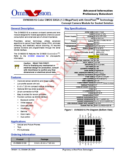
Advanced Information Preliminary DatasheetO mniTMisionOV9650S1G Color CMOS SXGA (1.3 MegaPixel) with OmniPixel TM TechnologyConcept Camera Module for Socket SolutionGeneral DescriptionKey SpecificationsOV9650S1GColor CMOS SXGA (1.3 MegaPixel) OmniPixel™ Camera ModuleO Functional DescriptionFigure 2 shows the functional block diagram of the OV9650S1G Camera Module. The OV9650S1G includes:•1/4"lens •OV9650 C AMERA C HIP image sensor •Socket connectorFigure 2 Functional Block DiagramFunctional DescriptionO Imaging SpecificationsTable 1Sensor Image FunctionsOV9650S1GColor CMOS SXGA (1.3 MegaPixel) OmniPixel™ Camera ModuleOPin DescriptionNOTE:Y[9:2] for 8-bit YUV or RGB (Y9 MSB, Y2 LSB)Y[9:0] for 10-bit RGB (Y9 MSB, Y0 LSB)Table 3Pin DescriptionPin NumberName Pin Type Function/Description01VSYNC Output Vertical sync output 02HREF Output HREF output 03PCLK Output Pixel clock output04DOVDD Power Digital power supply (V DD-IO = 2.5 to 3.3 VDC) for I/O05RESET Function (default = 0)Clears all registers and resets them to their default values. Active high, internal pull-down resistor.06Y9Output Output bit[9] - MSB for 10-bit RGB and 8-bit YUV 07Y7Output Output bit[7]08Y8Output Output bit[8]09Y6Output Output bit[6]10DGND Power Digital ground11Y1Output Output bit[1] - for 10-bit RGB only 12Y3Output Output bit[3]13Y5Output Output bit[5]14Y4Output Output bit[4]15Y2Output Output bit[2] - LSB for 8-bit YUV 16SIO_D I/O SCCB serial interface data I/O17AVDD Power Analog power supply (V DD-A = 2.45 to 2.8 VDC)18AGND Power Analog ground 19NC–Reserved - no connect20PWDNFunction (default = 0)Power Down Mode Selection - active high, internal pull-down resistor.0:Normal mode1:Power down mode 21SIO_C Input SCCB serial interface clock input22DVDD Power Power supply (V DD-C = 1.8 VDC + 10%) for digital core logic 23XVCLK1Input Crystal clock input24Y0OutputOutput bit[0] - LSB for 10-bit RGB onlyElectrical CharacteristicsOElectrical CharacteristicsNOTE:Exceeding the Absolute Maximum ratings shown above invalidates all AC and DC electrical specifications and may result in permanent device damage.Table 4Absolute Maximum RatingsAmbient Storage Temperature-40ºC to +95ºCSupply Voltages (with respect to Ground)V DD-A4.5 V V DD-C 3 V V DD-IO4.5 VAll Input/Output Voltages (with respect to Ground)-0.3V to V DD-IO +1V Lead Temperature, Surface-mount process +230ºC ESD Rating, Human Body model 2000VTable 5DC Characteristics (-20°C < T A < 70°C)Symbol ParameterConditionMin Typ Max Unit V DD-A DC supply voltage – Analog – 2.45 2.5 2.8V V DD-C DC supply voltage – Core – 1.62 1.8 1.98V V DD-IO DC supply voltage – I/O power – 2.25– 3.6V I DDA Active (Operating) Current See Note a a. V DD-A = 2.5V, V DD-C = 1.8V, V DD-IO = 3.0VI DDA = ∑{I DD-IO + I DD-C + I DD-A }, f CLK = 24MHz at 7.5 fps YUV output, no I/O loading20mA I DDS-SCCB Standby Current See Note b b. V DD-A = 2.5V, V DD-C = 1.8V, V DD-IO = 3.0VI DDS:SCCB refers to a SCCB-initiated Standby, while I DDS:PWDN refers to a PWDN pin-initiated Standby 1mA I DDS-PWDN Standby Current 10µA V IH Input voltage HIGH CMOS0.7 x V DD-IOV V IL Input voltage LOW 0.3 x V DD-IOV V OH Output voltage HIGH CMOS0.9 x V DD-IOV V OL Output voltage LOW 0.1 x V DD-IOV I OH Output current HIGH See Note cc.Standard Output Loading = 25pF, 1.2K Ω8mA I OL Output current LOW 15mA I LInput/Output LeakageGND to V DD-IO ± 1µAOV9650S1G Color CMOS SXGA (1.3 MegaPixel) OmniPixel™ Camera Module OTable 6 Functional and AC Characteristics (-20°C < T A < 70°C)Symbol Parameter Min Typ Max Unit Functional CharacteristicsA/D Differential Non-Linearity+ 1/2LSBA/D Integral Non-Linearity+1LSBAGC Range18dBRed/Blue Adjustment Range12dB Inputs (PWDN, CLK, RESET)f CLK Input Clock Frequency102448MHzt CLK Input Clock Period2142100ns t CLK:DC Clock Duty Cycle455055% t S:RESET Setting time after software/hardware reset1ms t S:REG Settling time for register change (10 frames required)300ms SCCB Timing (see Figure4)f SIO_C Clock Frequency400KHzt LOW Clock Low Period 1.3µs t HIGH Clock High Period600ns t AA SIO_C low to Data Out valid100900ns t BUF Bus free time before new START 1.3µs t HD:STA START condition Hold time600ns t SU:STA START condition Setup time600ns t HD:DAT Data-in Hold time0µs t SU:DAT Data-in Setup time100ns t SU:STO STOP condition Setup time600ns t R, t F SCCB Rise/Fall times300ns t DH Data-out Hold time50ns Outputs (VSYNC, HREF, PCLK, and Y[9:0] (see Figure5, Figure6, Figure7, Figure8, Figure10, and Figure11) t PDV PCLK[↓] to Data-out Valid5ns t SU Y[9:0] Setup time15ns t HD Y[9:0] Hold time8ns t PHH PCLK[↓] to HREF[↑]05ns t PHL PCLK[↓] to HREF[↓]05nsAC Conditions:• V DD: V DD-C = 1.8V, V DD-A = 2.5V, V DD-IO = 3.0V • Rise/Fall Times: I/O: 5ns, MaximumSCCB: 300ns, Maximum • Input Capacitance: 10pf• Output Loading: 25pF, 1.2KΩ to 3V• f CLK: 24MHzTiming SpecificationsOTiming SpecificationsFigure 4 SCCB Timing DiagramOV9650S1G Color CMOS SXGA (1.3 MegaPixel) OmniPixel™ Camera Module OFigure 7 VGA Frame TimingTiming SpecificationsOFigure 10 CIF Frame TimingOV9650S1G Color CMOS SXGA (1.3 MegaPixel) OmniPixel™ Camera Module OFigure 13 RGB 565 Output Timing DiagramRegister Set Table7 shows detailed descriptions of the Device Control registers. The device slave addresses for the OV9650S1G are 60 for write and 61 for read.Table 7 Device Control Register ListAddress (Hex)RegisterNameDefault(Hex)R/W Description00GAIN00RW AGC[7:0] – Gain control gain setting •Range: [00] to [FF]01BLUE80RW AWB – Blue channel gain setting •Range: [00] to [FF]02RED80RW AWB – Red channel gain setting •Range: [00] to [FF]03VREF12RW Vertical Frame ControlBit[7:6]:AGC[9:8] (see register GAIN for AGC[7:0])Bit[5:3]:VREF end low 3 bits (high 8 bits at VSTOP[7:0] Bit[2:0]:VREF start low 3 bits (high 8 bits at VSTRT[7:0]04COM100RW Common Control 1Bit[7]:ReservedBit[6]:CCIR656 formatBit[5]:QQVGA or QQCIF format. Effective only when QVGA or QCIF output is selected (register bit COM7[4]) and relatedHREF skip mode based on format is selected (registerCOM1[3:2])Bit[4]:ReservedBit[3:2]:HREF skip option00:No skip01:YUV/RGB skip every other row for YUV/RGB, skip 2rows for every 4 rows for Raw data1x:Skip 3 rows for every 4 rows for YUV/RGB, skip 6 rowsfor every 8 rows for Raw dataBit[1:0]:AEC low 2 LSB (see registers AECHM for AEC[15:10] and AECH for AEC[9:2])05BAVE00RW U/B Average LevelAutomatically updated based on chip output format06GEAVE00RW Y/Ge Average LevelAutomatically updated based on chip output format07RSVD00–Reserved08RAVE00RW V/R Average LevelAutomatically updated based on chip output format09COM201RW Common Control 2Bit[7:5]:ReservedBit[4]:Soft sleep modeBit[3:2]:ReservedBit[1:0]:Output drive capability00:1x01:2x10:2x11:4x0A PID96R Product ID Number MSB (Read only) 0B VER50R Product ID Number LSB (Read only)0C COM300RW Common Control 3Bit[7]:ReservedBit[6]:Output data MSB and LSB swapBit[5:4]:ReservedBit[3]:Pin selection1:Change RESET pin to EXPST_B (frame exposuremode timing) and change PWDN pin to FREX (frameexposure enable)Bit[2]:VarioPixel for VGA and CIFBit[1]:ReservedBit[0]:Single frame output (used for Frame Exposure mode only)0D COM400RW Common Control 4Bit[7]:VarioPixel for QVGA, QCIF, QQVGA, and QQCIFBit[6]:ReservedBit[5]:Pixels for sub-sampling mode0:Get average neighbor pixel in sub-sampling mode1:Get sum instead of average neghbor pixel insub-sampling modeBit[4:3]:ReservedBit[2]:Tri-state option for output clock at power-down period 0:Tri-state at this period1:No tri-state at this periodBit[1]:Tri-state option for output data at power-down period 0:Tri-state at this period1:No tri-state at this periodBit[0]:Reserved(Hex)Name(Hex)R/W Description0E COM501RW Common Control 5Bit[7]:System clock selection. If the system clock is 48 MHz, this bit should be set to high to get 15 fps for YUV or RGB Bit[6:5]:ReservedBit[4]:Slam mode enable0:Master mode1:Slam mode (used for slave mode)Bit[3]:ADC offset manual control0:Offset is controlled automatically1:Register OFON[7:4] can enable ADC offset addition Bit[2:1]:ReservedBit[0]:Exposure step can be set longer than VSYNC time1:In Normal mode, AEC changes by 1/16 and in Fastmode, AEC changes by double0F COM643RW Common Control 6Bit[7]:Output of optical black line option0:Disable HREF at optical black1:Enable HREF at optical black Bit[6:5]:ReservedBit[4]:HREF is high from optical black lineBit[3]:Enable bias for ADBLCBit[2]:ADBLC offset0:Use 4-channel ADBLC1:Use 2-channel ADBLCBit[1]:Reset all timing when format changes Bit[0]:Enable ADBLC option10AECH40RW Exposure ValueBit[7:0]:AEC[9:2] (see registers AECHM for AEC[15:10] and COM1 for AEC[1:0])11CLKRC00RW Data Format and Internal ClockBit[7]:Digital PLL option0:Disable double clock option, meaning the maximumPCLK can be as high as half input clock1:Enable double clock option, meaning the maximumPCLK can be as high as input clockBit[6]:Use external clock directly (no clock pre-scale available) Bit[5:0]:Internal clock pre-scalarF(internal clock) = F(input clock)/(Bit[5:0]+1)•Range: [0 0000] to [1 1111](Hex)Name(Hex)R/W Description12COM700RW Common Control 7Bit[7]:SCCB Register Reset0:No change1:Resets all registers to default valuesBit[6]:Output format - VGA selectionBit[5]:Output format - CIF selectionBit[4]:Output format - QVGA selectionBit[3]:Output format - QCIF selectionBit[2]:Output format - RGB selectionBit[1]:ReservedBit[0]:Output format - Raw RGB (COM7[2] must be set high)13COM88F RW Common Control 8Bit[7]:Enable fast AGC/AEC algorithmBit[6]:AEC - Step size limit (used only in fast condition and COM5[0] is low)0:Fast condition change maximum step is VSYNC1:Unlimited step sizeBit[5]:Banding filter ON/OFFBit[4]:ReservedBit[3]:Enable AEC time can be less than 1 line optionBit[2]:AGC EnableBit[1]:AWB EnableBit[0]:AEC Enable14COM94A RW Common Control 9Bit[7]:ReservedBit[6:4]:Automatic Gain Ceiling - maximum AGC value000:2x001:4x010:8x011:16x100:32x101:64x110:128xBit[3]:Exposure timing can be less than limit of banding filter when light is too strongBit[2]:Data format - VSYNC drop option0:VSYNC always exists1:VSYNC will drop when frame data drops Bit[1]:Enable drop frame when AEC step is larger than VSYNC Bit[0]:Freeze AGC/AEC(Hex)Name(Hex)R/W Description21GBOS80RW Gb channel ADBLC resultBit[7]:Offset adjustment sign0:Add offset1:Subtract offsetBit[6:0]:Offset value of 10-bit range22GROS80RW Gr channel ADBLC resultBit[7]:Offset adjustment sign0:Add offset1:Subtract offsetBit[6:0]:Offset value of 10-bit range23ROS80RW R channel ADBLC resultBit[7]:Offset adjustment sign0:Add offset1:Subtract offsetBit[6:0]:Offset value of 10-bit range24AEW78RW AGC/AEC - Stable Operating Region (Upper Limit) 25AEB68RW AGC/AEC - Stable Operating Region (Lower Limit)26VPT D4RW AGC/AEC Fast Mode Operating Region Bit[7:4]:Upper limit of 4 MSBBit[3:0]:Lower limit of 4 LSB27BBIAS80RW B Channel Signal Output Bias (effective only when COM6[0] = 1)Bit[7]:Bias adjustment sign0:Add bias1:Subtract biasBit[6:0]:Bias value of 10-bit range28GbBIAS80RW Gb Channel Signal Output Bias (effective only when COM6[0] = 1) Bit[7]:Bias adjustment sign0:Add bias1:Subtract biasBit[6:0]:Bias value of 10-bit range29Gr_COM00RW Analog BLC and Regulator Control Bit[7:6]:ReservedBit[5]:Bypass Analog BLCBit[4]:Bypass regulatorBit[3:0]:Reserved2A EXHCH00RW Dummy Pixel Insert MSBBit[7:4]: 4 MSB for dummy pixel insert in horizontal direction Bit[3:2]:HSYNC falling edge delay 2 MSBBit[1:0]:HSYNC rising edge delay 2 MSB2B EXHCL00RW Dummy Pixel Insert LSB8 LSB for dummy pixel insert in horizontal direction(Hex)Name(Hex)R/W Description2C RBIAS80RW R Channel Signal Output Bias (effective only when COM6[0] = 1) Bit[7]:Bias adjustment sign0:Add bias1:Subtract biasBit[6:0]:Bias value of 10-bit range2D ADVFL00RW LSB of insert dummy lines in vertical direction (1 bit equals 1 line) 2E ADVFH00RW MSB of insert dummy lines in vertical direction2F YAVE00RW Y/G Channel Average Value30HSYST08RW HSYNC Rising Edge Delay (low 8 bits)31HSYEN30RW HSYNC Falling Edge Delay (low 8 bits)32HREF A4RW HREF ControlBit[7:6]:HREF edge offset to data outputBit[5:3]:HREF end 3 LSB (high 8 MSB at register HSTOP) Bit[2:0]:HREF start 3 LSB (high 8 MSB at register HSTART)33CHLF00RW Bit[7:0]:Reserved 34ARBLM03RW Bit[7:0]:Reserved 35-36RSVD XX–Reserved37ADC04RW Bit[7:0]:Reserved 38ACOM12RW Bit[7:0]:Reserved39OFON00RW Bit[7:4]:ReservedBit[3]:Line buffer power down - must be set to "1" before chip power downBit[2:0]:Reserved3A TSLB0C RW Line Buffer Test OptionBit[7:6]:ReservedBit[5]:Bit-wise reverseBit[4]:UV output value0:Use normal UV output1:Use fixed UV value set in registers MANU and MANVas UV output instead of chip outputBit[3]:Output sequence is Y U Y V instead of U Y V YBit[2]:Output sequence is Y V Y U instead of Y U Y VBit[1]:ReservedBit[0]:Digital BLC(Hex)Name(Hex)R/W Description3B COM1100RW Common Control 11Bit[7]:Night mode0:Night mode disable1:Frame rate will adjust based on COM11[6:5] beforeAGC gain increases more than 2. Also,ADVFL andADVFL will be automatically updated.Bit[6:5]:Night mode insert frame option00:Normal frame rate01:1/2 frame rate10:1/4 frame rate11:1/8 frame rateBit[4:3]:Average calculation window option00:Use full frame01:Use half frame10:Use quarter frame11:Use lower two-thirdsBit[2:1]:ReservedBit[0]:Manual banding filter mode3C COM1240RW Common Control 12Bit[7]:HREF option0:No HREF when VREF is low1:Always has HREFBit[6:3]:ReservedBit[2]:Enable YUV averageBit[1:0]:Reserved3D COM1399RW Common Control 13Bit[7:6]:Gamma selection for signal00:No gamma function01:Gamma used for Y channel only10:Gamma used for Raw data before interpolation11:Not allowedBit[5]:ReservedBit[4]:Enable color matrix for RGB or YUVBit[3]:Enable Y channel delay option0:Delay UV channel1:Delay Y channelBit[2:0]:Output Y/UV delay3E COM140E RW Common Control 14Bit[7:2]:ReservedBit[1]:Enable edge enhancement for YUV output (effective only for YUV/RGB, no use for Raw data)Bit[0]:Edge enhancement option0:Edge enhancement factor = EDGE[3:0]1:Edge enhancement factor = 2 x EDGE[3:0](Hex)Name(Hex)R/W Description3F EDGE88RW Edge Enhancement AdjustmentBit[7:4]:Edge enhancement threshold[3:0](see register COM22[7:6} for Edge threshold[5:4]) Bit[3:0]:Edge enhancement factor40COM15C0RW Common Control 15Bit[7:6]:Data format - output full range enable0x:Output range: [10] to [F0]10:Output range: [01] to [FE]11:Output range: [00] to [FF]Bit[5:4]:RGB 555/565 option (must set COM7[2] high) x0:Normal RGB output01:RGB 56511:RGB 555Bit[3]:Swap R/B in RGB565/RGB555 formatBit[2:0]:Reserved41COM1610RW Common Control 16Bit[7:2]:ReservedBit[1]:Color matrix coefficient double option Bit[0]:Reserved42COM1708RW Common Control 17Bit[7:5]:ReservedBit[4]:Edge enhancement optionBit[3]:ReservedBit[2]:Select single frame outBit[1]:Tri-state outputBit[0]:Reserved43-4E RSVD XX–Reserved4F MTX158RW Matrix Coefficient 1 50MTX248RW Matrix Coefficient 2 51MTX310RW Matrix Coefficient 3 52MTX428RW Matrix Coefficient 4 53MTX548RW Matrix Coefficient 5 54MTX670RW Matrix Coefficient 6 55MTX740RW Matrix Coefficient 7 56MTX840RW Matrix Coefficient 8 57MTX940RW Matrix Coefficient 958MTXS0F RW Matrix Coefficient Sign for coefficient 9 to 2 0:Plus1:Minus59-61RSVD XX–Reserved(Hex)Name(Hex)R/W Description62LCC100RW Lens Correction Option 163LCC200RW Lens Correction Option 264LCC310RW Lens Correction Option 365LCC480RW Lens Correction Option 466LCC500RW Lens Correction Control67MANU80RW Manual U Value (effective only when register TSLB[4] is high) 68MANV80RW Manual V Value (effective only when register TSLB[4] is high)69HV00RW Manual Banding Filter MSBBit[7:1]:ReservedBit[0]:Matrix coefficient 1 sign6A MBD00RW LSB of Banding Filter Value (effective only when COM11[0] is high). 6B DBLV0A RW Bit[7:0]:Reserved6C-7B GSP XX RW Gamma curve7C-8A GST XX RW Gamma curve8B COM2104RW Common Control 21Bit[7:4]:ReservedBit[3]:VGA option - use VGA window modeBit[2]:ReservedBit[1]:Digital BLC optionBit[0]:UV channel uses sum or average of neighbor pixel in sub-sampling mode8C COM2200RW Common Control 22Bit[7:6]:Edge enhancement threshold[5:4](see register EDGE[7:4} for Edge threshold[3:0]) Bit[5]:De-noise enableBit[4:2]:ReservedBit[1]:White-pixel erase enableBit[0]:White-pixel erase option8D COM2300RW Common Control 23Bit[7:5]:ReservedBit[4]:Color bar test modeBit[3:2]:ReservedBit[1]:Digital AWB enableBit[0]:Reserved8E COM2400RW Common Control 24Bit[7:0]:Reserved(Hex)Name(Hex)R/W DescriptionRegister SetO8F DBLC10F RWDigital BLC Offset SignBit[7:4]:ReservedBit[3]:Digital BLC B offset sign Bit[2]:Digital BLC R offset sign Bit[1]:Digital BLC Gb offset sign Bit[0]:Digital BLC Gr offset sign90DBLC_B 00RWDigital BLC B Channel Offset ValueBit[7:0]:Digital BLC B channel offset value91DBLC_R 00RWDigital BLC R Channel Offset ValueBit[7:0]:Digital BLC R channel offset value92DM_LNL 00RWDummy Line low 8 bitsBit[7:0]:Control insert Dummy line[7:0]93DM_LNH 00RW Dummy Line high 8 bitsBit[7:0]:Control insert Dummy line[15:8]94-9C RSVD XX –Reserved9D LCCFB 00RW Lens Correction B Channel Control 9E LCCFR 00RW Lens Correction R Channel Control 9FDBLC_Gb00RWDigital BLC Gb Channel Offset ValueBit[7:0]:Digital BLC Gb channel offset value A0DBLC_Gr 00RWDigital BLC Gr Channel Offset ValueBit[7:0]:Digital BLC Gr channel offset valueA1AECHM40RWExposure Value - AEC MSB 5 bitsBit[7:6]:ReservedBit[5:0]:AEC[15:10] (see registers AECH for AEC[9:2] and COM1 for AEC[1:0])A2-A3RSVD XX –ReservedA4COM2500RWCommon Control 25Bit[7:0]:ReservedA5COM2600RWCommon Control 26Bit[7:0]:ReservedA6G_GAIN 80RWGreen Gain OptionBit[7:0]:Green gain when using digital AWBA7VGA_ST 14RW Vertical Start Point for VGABit[7:0]:Define vertical start point in VGA sub-windowing modeA8-AAACOMXX–ReservedNOTE: All other registers are factory-reserved. Please contact OmniVision Technologies for reference register settings.Table 7Device Control Register List (Continued)Address (Hex)Register NameDefault (Hex)R/WDescription8.008.00AA1.50s4.507.20s6.20SECTION A-ALensLens HolderKey for image orientationPCBImage PlaneImage Sensor6.606.6010.20Package SpecificationsOMechanical SpecificationsConnector InformationThe OV9650S1G uses a 24-pin socket connector. Table 9 shows a listing of some recommended connectors.Optical SpecificationsTable 8Mechanical DimensionsParameterSpecification CommentsSensor 5.1 mm x 5.72 mm CMOS in housingLensGlass/Plastic Connection Type 10.2 x 10.2 x 4.5 mm SMK socket (consult OmniVision for details)Module Housing8 mm x 8 mm x 7.20 mmTable 9 Recommended ConnectorsManufacturerPart No.DescriptionSMKCLE9024-0201E CLE9024-0301F T-54-10499T-347379-JIGUSocket connector Shield case (optional)Socket without locking mechanism (for testing purposes)Module extraction jigTable 10Optical SpecificationsParameterSpecification CommentsLens Elements Glass/Plastic Hybrid1 glass, 3 plastic (aspheric) fixed focusViewing Angle 60° diagonal Focal Length 4.7 mm F Number 2.8Focus Range 30 cm → ∞FilterIR cut IncludedMount Description M7 x 0.35P TV Distortion 0.51%Focus AdjustmentFixed80 cmOV9650S1GColor CMOS SXGA (1.3 MegaPixel) OmniPixel™ Camera ModuleOHandling Precautions•DO NOT try to open the unit enclosure as there is no user-serviceable component inside.•To prevent damage to the camera module by electrostatic discharge, handle the camera module ONLY after discharging ALL static electricity from yourself and ensuring a static-free environment for the camera module.•DO NOT touch the top surface of the lens.•DO NOT press down on the lens.•DO NOT try to focus the lens.•DO NOT put the camera module in a dusty environment.•To reduce the risk of electrical shock and damage to the camera module, turn OFF the power before connect and disconnect the camera module.•DO NOT drop the camera module more than 60 cm onto any hard surface.•To prevent fire or shock hazard, DO NOT expose camera module to rain or moisture.•DO NOT expose camera module to direct sunlight.•DO NOT put camera module in a high temperature environment.•DO NOT use liquid or aerosol cleaners to clean the lens.•DO NOT make any changes or modifications to camera module.•DO NOT subject camera module to strong electromagnetic field.•DO NOT subject the camera module to excessive vibration or shock.WARNING: READ THIS FIRST!Prior to handling any OmniVision camera module, read the following precautions.Handling PrecautionsONote:•All information shown herein is current as of the revision and publication date. Please refer to the OmniVision web site ( ) to obtain the current versions of all documentation.•OmniVision Technologies, Inc. reserves the right to make changes to their products or todiscontinue any product or service without further notice (It is advisable to obtain current product documentation prior to placing orders).•Reproduction of information in OmniVision product documentation and specifications is permissible only if reproduction is without alteration and is accompanied by all associated warranties, conditions, limitations and notices. In such cases, OmniVision is not responsible or liable for any information reproduced.•This document is provided with no warranties whatsoever, including any warranty of merchantability, non-infringement, fitness for any particular purpose, or any warranty otherwise arising out of any proposal, specification or sample. Furthermore, OmniVision Technologies Inc. disclaims all liability, including liability for infringement of any proprietary rights, relating to use of information in this document. No license, expressed or implied, by estoppels or otherwise, to any intellectual property rights is granted herein.•‘OmniVision’, ‘CameraChip’, and ’OmniPixel’ are trademarks of OmniVision Technologies, Inc. All other trade, product or service names referenced in this release may be trademarks orregistered trademarks of their respective holders. Third-party brands, names, and trademarks are the property of their respective owners.For further information, please feel free to contact OmniVision at info@ .OmniVision Technologies, Inc.1341 Orleans Drive Sunnyvale, CA USA (408) 542-3000OV9650S1G Color CMOS SXGA (1.3 MegaPixel) OmniPixel™ Camera Module O。

NVP2650和NVP2650D
NVP2650和NVP2650D区别之处是后者是双目,前者是单目,目前只有NVP2650+OV2775配套使用,另外一种方案是NVP2650+IMX390,具体区别如下:
一、NVP2650
1、最大分辨率2 m@60fps
2、MIPI支持通用汽车摄像头ISP
3、NVP2650是具有MIPI的FHD@60fps摄像头ISP,支持汽车摄像头所需的选定功能。
NVP2650适用于无极相机、座舱相机、环视监控相机等。
高动态范围支持LFM(LED闪烁抑制)双像素传感器。
关键特性:
1、HDR
2、LFM
3、Full HD
4、先进的信号过滤
适用的线缆:
CVBS LVDS AHD
二、NVP2650D
1、1920 x1280@30fps (ch) 1920 x1080@60fps (1 ch) ISO26262 ASIL-B合规
2、2个isp在一个芯片组
3、符合ISO26262 - ASIL B(汽车安全完整性等级)
2 in 1 -单片机支持2ch。
相机的解决方案配置
分辨率-每个ISP支持2.5M, FHD 2ch.@30fps
功能- LFM(LED闪烁缓解)通过特定的CMOS传感器关键特性:
1、D-WDR:数字宽动态
2、LFM
3、DFOG
4、ASIL-B
5、144BGA (9mm×9mm)传输模式:MIPI
Q-Q:8721-9158
TE-LL:15110-264-988。
ov感光芯片OV感光芯片是一种光电转化器件,它能将光信号转化为电信号。
目前市面上常见的OV感光芯片有OV5648、OV8865等型号,它们都具有高像素、高灵敏度等特点,广泛应用于数码相机、手机摄像头等领域。
OV感光芯片的工作原理是基于光敏二极管的光电效应。
当光照射到芯片上时,光能会激发器件中的载流子,形成一定的电流。
而感光芯片通过读取这个电流的大小,来确定光的强弱和颜色信息。
根据这个原理,OV感光芯片能够将光的信息转化为电信号,进而实现图像的捕捉和处理。
随着科技的不断进步和人们对图像质量要求的提高,OV感光芯片从最开始的低像素、低灵敏度发展到了如今的高像素、高灵敏度。
比如,OV5648是一款500万像素的感光芯片,具有1.4μm的像素尺寸和6400mV/Lux-s的灵敏度。
这使得它能够在低光照条件下获得更好的图像质量,满足用户对高清拍摄的需求。
OV感光芯片的高像素和高灵敏度离不开光学和电子技术的不断进步。
一方面,光学技术的进步让OV感光芯片能够实现更小的像素尺寸,增加感光面积,提高感光能力。
另一方面,电子技术的进步使得OV感光芯片能够更好地处理和传输电信号,提高图像的清晰度和稳定性。
除了高像素和高灵敏度,OV感光芯片还具有一些其他的优势。
首先,它具有较低的功耗和较高的工作效率,能够节约电力资源,延长电池使用时间。
其次,它具有较小的尺寸和较轻的重量,方便集成在各种设备中,如手机、平板电脑等。
此外,在图像的处理和传输方面,OV感光芯片还支持高动态范围(HDR)功能和视频图像稳定器(VIS)功能,提高图像的质量和稳定性。
然而,OV感光芯片也存在一些不足之处。
例如,由于其感光面积有限,当光线较弱或者场景较暗时,图像容易出现噪点和暗部细节不足的问题。
此外,由于OV感光芯片主要应用在手机摄像头领域,对于大型成像设备,如数码相机和监控摄像机等,其像素和灵敏度等性能还有待提高。
总的来说,OV感光芯片作为一种光电转化器件,具有高像素、高灵敏度等优势,被广泛应用于数码相机、手机摄像头等领域。
OV7670-CMOS摄像头使用说 明2014.2.10 参赛平台1.OV7670带FIFO 模块1.简介:OV7670带FIFO 模块,是针对慢速的MCU 能够实现图像采集控制推出的带有缓冲存储空间的一种模块。
这种模块增加了一个FIFO (先进先出)存储芯片,同样包含30w 像素的CMOS 图像感光芯片,3.6mm 焦距的镜头和镜头座,板载CMOS 芯片所需要的各种不同电源(电源要求详见芯片的数据文件),板子同时引出控制管脚和数据管脚,方便操作和使用。
图1.OV7670带FIFO模块 2.管脚定义:参赛平台如图,控制传感器所需的管脚定义如下:3V3-----输入电源电压(推荐使用3.3,5V 也可,但不推荐)GDN-----接地点SIO_C---SCCB 接口的控制时钟(注意:部分低级单片机需要上拉控制,和I2C 接口类似)SIO_D---SCCB 接口的串行数据输入(出)端(注意:部分低级单片机需要上拉控制,和I2C 接口类似) VSYNC---帧同步信号(输出信号)HREF----行同步信号(输出信号)PCLK----像素时钟(输出信号)XCLCK---时钟信号(输入信号)D0-D7---数据端口(输出信号)RESTE---复位端口(正常使用拉高)PWDN----功耗选择模式(正常使用拉低)STROBE—拍照闪光控制端口(正常使用可以不需要)FIFO_RCK---FIFO 内存读取时钟控制端FIFO_WR_CTR----FIFO 写控制端(1为允许CMOS 写入到FIFO,0为禁止) FIFO_OE----FIFO 关断控制FIFO_WRST—FIFO 写指针服务端FIFO_RRST—FIFO 读指针复位端 参赛平台图7.FIFO摄像头接口定义3.控制方式说明由于采用了FIFO 做为数据缓冲,数据采集大大简便,用户只需要关心是如何读取即可,不需要关心具体数据是如何采集到的,这样可减小甚至不用关心CMOS 的控制以及时序关系,就能够实现图像的采集。
Contents一、手机CAMERA的物理结构:........................................................................................ - 4 -二、 CAMERA 的成像原理: ................................................................................................. - 4 -三、 CAMERA 常见的数据输出格式:.................................................................................. - 5 -四、阅读CAMERA的规格书(以TRULY模组OV5647_RAW为例):........................... - 6 -五、 CAMERA 的硬件原理图及引脚 ..................................................................................... - 7 -1、电源部分:.................................................................................................................... - 7 -2、 S ENSOR I NPUT部分:................................................................................................... - 7 -3、 S ENSOR O UT P UT部分:............................................................................................... - 7 -4、 I2C 部分:SCL,I2C时钟信号线和SDA,I2C数据信号线。
废话后面说,先直接上OV7670寄存器的配置部分const uint8_t OV7670_Reg[][2]={//Frame Rate Adjustment for 24Mhz input clock//30fps PCLK=24MHz{0x11, 0x80},//软件应用手册上设置的是0x80,例程设置的是0x00{0x6b, 0x0a},//PLL控制,软件应用手册上设置的是0x0a,例程设置的是0x40,将PLL调高的话就会产生花屏{0x2a, 0x00},{0x2b, 0x00},{0x92, 0x00},{0x93, 0x00},{0x3b, 0x0a},//Output format{0x12, 0x14},//QVGA(320*240)、RGB//RGB555/565 option(must set COM7[2] = 1 and COM7[0] = 0){0x40, 0x10},//RGB565,effective only when RGB444[1] is low{0x8c, 0x00},//Special effects - 特效//normal{0x3a, 0x04},{0x67, 0xc0},{0x68, 0x80},//Mirror/VFlip Enable - 水平镜像/竖直翻转使能{0x1e, 0x37},//修改配置值将产生图像显示上下或左右颠倒//Banding Filter Setting for 24Mhz Input Clock - 条纹滤波器//30fps for 60Hz light frequency//{0x13, 0xe7},//banding filer enable//{0x9d, 0x98},//50Hz banding filer//{0x9e, 0x7f},//60Hz banding filer//{0xa5, 0x02},//3 step for 50Hz//{0xab, 0x03},//4 step for 60Hz//{0x3b, 0x02},//select 60Hz banding filer//Simple White Balance - 白平衡//{0x13, 0xe7},//AWB、AGC、AGC Enable and ...//{0x6f, 0x9f},//simple AWB//AWBC - 自动白平衡控制(Automatic white balance control)//{0x43, 0x14},//用户手册里这些寄存器的值都是保留(Reserved),不用设置的呀?//{0x44, 0xf0},//{0x45, 0x34},//{0x46, 0x58},//{0x47, 0x28},//{0x48, 0x3a},//AWB Control//{0x59, 0x88},//用户手册连寄存器都是保留,初始值都没提供//{0x5a, 0x88},//{0x5b, 0x44},//{0x5c, 0x67},//{0x5d, 0x49},//{0x5e, 0x0e},//AWB Control//{0x6c, 0x0a},//{0x6d, 0x55},//{0x6e, 0x11},//{0x6f, 0x9f},//AGC/AEC - Automatic Gain Control自动增益补偿/Automatic exposure Control自动曝光控制//{0x00, 0x00},//{0x14, 0x20},//{0x24, 0x75},//{0x25, 0x63},//{0x26, 0xA5},//AEC algorithm selection - AEC公式选择//{0xaa, 0x94},//基于平均值的AEC算法Average-based AEC algorithm/基于直方图的AEC算法Histogram-based AEC algorithm//基于直方图的AGC/AEC的控制//{0x9f, 0x78},//{0xa0, 0x68},//{0xa6, 0xdf},//{0xa7, 0xdf},//{0xa8, 0xf0},//{0xa9, 0x90},//Fix Gain Control - 固定增益控制//{0x69, 0x5d},//Fix gain for Gr channel/for Gb channel/for R channel/for B channel//Color saturation 颜色饱和度+ 0//{0x4f, 0x80},//{0x50, 0x80},//{0x51, 0x00},//{0x52, 0x22},//{0x53, 0x5e},//{0x54, 0x80},//{0x58, 0x9e},//Brightness - 亮度+ 0//{0x55, 0x00},//Contrast - 对比度+ 0//{0x56, 0x40},//Gamma Curve - 伽马曲线//{0x7a, 0x20},//{0x7b, 0x1c},//{0x7c, 0x28},//{0x7d, 0x3c},//{0x7e, 0x55},//{0x7f, 0x68},//{0x80, 0x76},//{0x81, 0x80},//{0x82, 0x88},//{0x83, 0x8f},//{0x84, 0x96},//{0x85, 0xa3},//{0x86, 0xaf},//{0x87, 0xc4},//{0x88, 0xd7},//{0x89, 0xe8},//Matrix Coefficient - 色彩矩阵系数//{0x4f, 0x80},//{0x50, 0x80},//{0x51, 0x00},//{0x52, 0x22},//{0x53, 0x5e},//{0x54, 0x80},//Lens Correction Option - 镜头补偿选项 //{0x62, 0x00},//{0x63, 0x00},//{0x64, 0x04},//{0x65, 0x20},//{0x66, 0x05},//{0x94, 0x04},//effective only when LCC5[2] is high//{0x95, 0x08},//effective only when LCC5[2] is high//注释这些配置的话,就倾斜显示,并显示多块,这到底是控制什么的?跟时序图有关?{0x17, 0x16},//行频Horizontal Frame开始高八位(低三位在HREF[2:0]){0x18, 0x04},//行频Horizontal Frame结束高八位(低三位在HREF[5:3]){0x19, 0x02},//场频Vertical Frame开始高八位(低二位在VREF[1:0]){0x1a, 0x7b},//场频Vertical Frame结束高八位(低二位在VREF[3:2]){0x32, 0x80},//HREF{0x03, 0x06},//VREF//注释这个配置的话,就显示花屏了{0x15, 0x02},//配置PCLK、HREF、VSYNC相关//Automatic black Level Compensation - 自动黑电平校正{0xb0, 0x84},//调试时注释这项配置时,颜色显示不正常了,红色练绿色,绿色变红色,但用户手册对这寄存器是保留RSVD//{0xb1, 0x0c},//{0xb2, 0x0e},//{0xb3, 0x82},//{0xb8, 0x0a},//SCALING_xx寄存器//{0x70, 0x00},//{0x71, 0x00},//{0x72, 0x11},//{0x73, 0x08},//{0x3e, 0x00},//ADC//{0x37, 0x1d},//ADC控制ADC Control//{0x38, 0x71},//ADC和模拟共模控制ADC and Analog Common Mode Control//{0x39, 0x2a},//ADC偏移控制ADC Offset Control//零杂的寄存器//{0x92, 0x00},//空行低八位Dummy Line low 8 bits//{0xa2, 0x02},//像素时钟延时//{0x0c, 0x0c},//{0x10, 0x00},//{0x0d, 0x01},//{0x0f, 0x4b},//{0x3c, 0x78},//{0x74, 0x19},//用户手册里这几个寄存器都是保留RSVD//{0x0e, 0x61},//{0x16, 0x02},//{0x21, 0x02},//{0x22, 0x91},//{0x29, 0x07},//{0x33, 0x0b},//{0x35, 0x0b},//{0x4d, 0x40},//{0x4e, 0x20},//{0x8d, 0x4f},//{0x8e, 0x00},//{0x8f, 0x00},//{0x90, 0x00},//{0x91, 0x00},//{0x96, 0x00},//{0x9a, 0x80},};刚开始学OV7670摄像头,我想大家跟我一样心里很毛躁吧,一个模块需要你配置100多个寄存器,但用户手册对寄存器的介绍却草草的一笔带过,自己无从下手啊,只能看开发板给的例程和上网找一些大虾的帖子了。
OV2650 Camera Module Hardware Application NotesLast Modified: Jan. 09th , 2009Document Revision: 1.03OmniVision Technologies, Inc. reserves the right to make changes without further notice to any product herein to improve reliability, function or design. OmniVision does not assume any liability arising out of the application or use of any project, circuit described herein; neither does it convey any license under its patent nor the right of others.This document contains information of a proprietary nature. None of this information shall be divulged to persons other than OmniVision Technologies, Inc. employee authorized by the nature of their duties to receive such information, or individuals or organizations authorized by OmniVision Technologies, Inc.OVTCo n f i de n t i a lTable of Contents1. OV2650 Camera Module Reference Design....................................................................................32. OV2650 Camera Interface Reference for Camera Phone................................................................32.1 Pin Definition.............................................................................................................................32.2 Power Supply.............................................................................................................................43. OV2650 Camera Operation..............................................................................................................53.1 Power Saving Modes.................................................................................................................53.2 Camera Operation in Power Down Mode..................................................................................53.2.1 Battery On..........................................................................................................................53.2.2 Wake up From Power Down..............................................................................................73.2.3 Power Down.......................................................................................................................73.3 Camera Operation in Power Off Mode......................................................................................83.3.1 Battery On..........................................................................................................................83.3.2 Camera On.........................................................................................................................83.3.3 Camera Off.........................................................................................................................93.3.4 Software Power down ...................................................................................................94. SCCB Bus sharing..........................................................................................................................105. Timing Considerations for Phone PCB Design..............................................................................115.1 Sample with PCLK..................................................................................................................115.2 Sample with XCLK.................................................................................................................125.3 Using EMI/ESD Device...........................................................................................................126. Hardware Check List......................................................................................................................136.1 Check Hardware Design..........................................................................................................136.1.1 Module Function..............................................................................................................136.1.2 Check Camera Interface of Phone....................................................................................136.2 Check if Camera Module is Working......................................................................................136.3 Check SCCB............................................................................................................................146.4 Check Camera Interface...........................................................................................................146.5 Some Typical Issues................................................................................................................156.6 Image Direction.......................................................................................................................166.6.1 Sensor 4:3, LCD 3:4.........................................................................................................166.6.2 Sensor 3:4, LCD 3:4.........................................................................................................166.7 Check Color/Brightness...........................................................................................................166.8 Check Image Center.. (17)OVTCo n f i de n t i a l1. OV2650 Camera Module Reference DesignNOTE:PWDN should be connected to ground if unused.RESETB should be connected to DOVDD outside of module if unused.AVDD is 2.45-3.0V sensor analog power(clean).DVDD is 1.5V+/- 10% sensor digital power(clean).DOVDD is 1.7V - 3.0V sensor digital IO power(clean).Sensor AGND and DGND should be separated and connect to a single point at outside PCB (Don't connect inside module).Decoupling capacitors should be close to the related sensor pins.C1 and C2 are for the two DVDDs.D9:D2 is module YUV and RGB 8bits output (D9:MSB, D2:LSB).D9:D0 is module raw RGB 10 bits output (D9:MSB, D0:LSB).2. OV2650 Camera Interface Reference for Camera Phone2.1 Pin DefinitionOV2650 has 10-bit video port, D[9:0]. For 10-bit RGB raw output, D[9:0] are used. For 8-bit YCbCr, 8bits RGB raw or 8-bits RGB 565 output, only D[9:2] are used. It support CCIR656 output too.The Href and Hsync signal is on the same pin – Href pin. The function of this pin could be selected as either Href function or Hsync function by SCCB setting.The SIO_C and SIO_D bus should have external pull up resistors, the typical value of the pull up resistors is about 4.7K.Resetb is active low. It can be controlled by a GPIO, or connected to DOVDD if not used. If Resetb is connected to DOVDD, the OV2650 camera module could be reset by SCCB setting.OVTCo n f i de n t i a lPWDN is active high. It can be controlled by a GPIO, or connected to DGND if not used.2.2 Power SupplyIf DOVDD uses different power supply than AVDD, then 3 regulators should be used.If DOVDD = AVDD = 2.8V, then only 2 regulators are required. R/C filter is used to separate AVDD from DOVDD.Note:a. The AGND and DGND should be separate inside module and connected together on phone PCB very close to camera module connector.b. DVDD is not used if using internal regulator. It is recommended to supply DVDD by external regulator to get better picture performance.c. If DVDD is supplied by internal regulator, DOVDD and AVDD should be turned on at the same time. If DOVDD and AVDD are applied separately, the power on sequence should be DOVDD first, then AVDD. The delay between DOVDD and AVDD should be as short as possible.OVTCo n f i de n t i a l3. OV2650 Camera Operation3.1 Power Saving ModesThere are 2 kind of power saving modes: power down mode and power off mode.Power down mode means that in power saving mode, all the power supplies to the camera module are kept. The camera is set into power down mode by pull high PWDN. At this time,sensor only have about 30UA standby current. In power down mode, all output pin can be treated as GPIO control.Power off mode means that in power saving mode, all the power supplies to the camera module are cut.3.2 Camera Operation in Power Down Mode3.2.1 Battery Ont1: from powers on to Reset pull high, >= 3mst2: from XCLK applied to SCCB software reset, >= 100ms t3: from SCCB software reset to SCCB initialization, >= 5ms t4: from PWDN pull high to XLCK pull low, >= 0.1msStep 1:Resetb is applied to OV2650 camera module. Applying a hard reset upon power up is required.Step 2:DOVDD, DVDD and AVDD powers are applied. OVTCo n f i de n t i a lIf DVDD is supplied by external power supply, there is no special requirement for power on sequence. If DVDD is generated by internal regulator, then AVDD should be supplied at the same time as DOVDD. If DOVDD and AVDD are applied separately, the power on sequence should be DOVDD first, then AVDD. The delay between DOVDD and AVDD should be as short as possible .Step 3:after 3ms of last power applied, pull high Reset.Step 4:Apply XCLK.Step 5:After 100ms, apply software reset by SCCB writing.Sccb_Slave_Address = 0x60; write_sccb16(0x3012, 0x80);Step 6:After 5ms, initialize OV2650 by SCCB initialization. Please find initialization setting from “OV2650 Camera Module Software Application Notes” or contact OmniVision local FAE. Step 7:Sccb_Slave_Address = 0x60; write_sccb16(0x30ab, 0x00); write_sccb16(0x30ad, 0x0a); write_sccb16(0x30ae, 0x27); write_sccb16(0x363b, 0x01);Pull high PWDN to DOVDD. Set OV2650 to power down mode.Step 8:After 0.1ms, Pull XCLK low.After battery on, OV2650 cameras should be set to power down mode to minimize power consumption. The cameras should be initialized first, then set to power down mode. OV2650 should be stay in power down mode for more than 1 frame time.OVTCo n f i de n t i a l3.2.2 Wake up From Power DownStep 1:Apply XCLKStep 2:after 0.1ms, Pull Low PWDNOptional Step 3:Restore register values to original values before power down.After wakeup, if MIPI connection direction function is needed, restore register 0x363b to its original value.3.2.3 Power DownStep 1:Sccb_Slave_Address = 0x60; write_sccb16(0x30ab, 0x00); write_sccb16(0x30ad, 0x0a); write_sccb16(0x30ae, 0x27); write_sccb16(0x363b, 0x01);Pull high PWDN to DOVDD. Set OV2650 to power down mode. Step 2:after 0.1ms, Pull XCLK lowPWDN SIO_CSIO_DXCLK PWDN SIO_C SIO_DXCLK Co n f i de n t i a l3.3 Camera Operation in Power Off Mode 3.3.1 Battery OnNo operation. Camera module is power off.3.3.2 Camera Ont1: from powers on to Reset pull high, >= 3mst2: from XCLK applied to SCCB software reset, >= 100ms t3: from SCCB software reset to SCCB initialization, >= 5msStep 1:DOVDD, DVDD and AVDD powers are applied.If DVDD is supplied by external power supply, there is no special requirement for power on sequence. If DVDD is generated by internal regulator, then AVDD should be supplied at the same time as DOVDD. If DOVDD and AVDD are applied separately, the power on sequence should be DOVDD first, then AVDD. The delay between DOVDD and AVDD should be as short as possible.Step 2:DOVDD, DVDD and AVDD powers are applied. Because OV2650 has on-chip initial power up reset features, not require special power supply sequence.Step 3:after 3ms of last power applied, pull high Reset.Step 4:Apply XCLK. OVTCo n f i de n t i a lStep 5:After 100ms, apply software reset by SCCB writing.Sccb_Slave_Address = 0x60; write_sccb16(0x3012, 0x80);Step 6:After 3ms, initialize OV2650 by SCCB initialization. Please find initialization setting from “OV2650 Camera Module Software Application Notes”or contact OmniVision local FAE.3.3.3 Camera OffStep 1.Pull low XCLK,Step 2.Pull Low RESET.Step 3.Turn off AVDD, DVDD and DOVDD.3.3.4 Software Power downSoftware power down not halt internal device clock, only halt internal circuit activity.Enter into Sleep(software power down)mode Sccb_Slave_Address = 0x60; write_sccb16(0x30ad, 0x00); write_sccb16(0x3086, 0x00); Wake up from Sleep mode Sccb_Slave_Address = 0x60; write_sccb16(0x30ad, 0x0a);DOVDD DVDDAVDD XCLK Reset PWDNOVTCo n f i dn t i a lwrite_sccb16(0x3086, 0x0f);4. SCCB Bus sharingThe SCCB bus of OV2650 camera module could share with other I2C device. When OV2650 is working, the read/write operation is separated by device address. The device address of OV2650 is 0x60. I2C read/write to address other than the 2 address above will not affect SCCB registers of OV2650. OV2650 has 16bits register address and 8bits register values.The SCCB bus of OV2650 could be shared with other devices in both power down mode and power off mode. When OV2650 camera module is power down or power off, the SCCB Bus is leave free. The SCCB of OV2650 doesn't affect the read/write of other I2C device.5. Timing Considerations for Phone PCB DesignThere are 2 clock signal for OV2650 camera module. One is the main clock (input clock) XCLK, the other is the pixel clock (output clock) PCLK. Some backend/baseband chips may use XCLK as pixel sample clock, some backend/baseband chips may use PCLK as pixel sample clock. It is recommended to use PCLK as pixel sample clock.Let's look at the clock distribution first.So the delay of video data to clock at backend/baseband side is very critical for timing design. If the delay is over the spec. of backend/baseband chip, the backend/baseband chip can not get video data correctly. The incorrect video data may have wrong color, fixed or moving horizontal lines. From the clock distribution diagram above, the delays are: Delay_XCLK = 0Delay_PCLK = PCB_Delay_XCLK + Internal_Delay + PLL_Delay + PCB_Delay_PCLKde n t i a lDelay_Data = PCB_Delay_XCLK + Internal_Delay + PLL_Delay + PCLK_to_Data_Delay + PCB_Delay_Data5.1 Sample with PCLKIf Backend/baseband sample video data with PCLK, the clock data delay is clock_data_delay = Delay_Data – Delay_PCLK= PCLK_to_Data_Delay + PCB_Delay_Data – PCB_Delay_PCLKThe clock data delay is not related with PCB delay of XCLK.If PCB is carefully designed so that the wire length of PCLK and Data are same, then PCB_Delay_Data = PCB_Delay_PCLK, the clock data delay is clock_data_delay = PCLK_to_Data_Delay, not related to PCB layout5.2 Sample with XCLKIf Backend/baseband sample video data with PCLK, the clock data delay is clock_data_delay = Delay_Data – Delay_XCLK= PCB_Delay_XCLK + Internal_Delay + PLL_Delay + PCLK_to_Data_Delay + PCB_Delay_DataThe data to clock delay at Baseband/Backend chip are much bigger than sampled with PCLK.And the delay is highly depend on PCB layout. So if XCLK is used to sample video data, it is very likely to have timing issue which would cause incorrect video data.5.3 Using EMI/ESD DeviceIf EMI/ESD device are used in phone design, the PCB delay increase very much. It should be very careful to manipulate the delays to meet timing spec. of backend/baseband chips.1.Try to use PCLK as sample clock of video data.2.XCLK and PCLK should not share ESD/EMI device with other signals. Use dedicate ESD/EMI device or R/C filters for XCLK and PCLK. So that the delay on XCLK and PCLK could be adjusted later.3.For camera module, use single ESD/EMI device or single R/C filter for XCLK and PCLK to minimize clock delay.4.Carefully layout PCB to keep XCLK wire as short as possible, PCLK wire the same length as data lines.5.Minimize the length of FPC of camera module.OVTCo n f i de n t i a l6. Hardware Check List6.1 Check Hardware Design 6.1.1 Module FunctionCheck camera module function with USB 2.0 test board (Module interface board may be needed, please contact with module maker). The module should display image correctly on PC.Check module schematic design, pin definition match with camera interface of phone. Analog ground and digital ground are separated inside camera module.6.1.2 Check Camera Interface of PhonePin definition matches with camera module design.AVDD is supplied by separate regulator. DVDD and DOVDD could be supplied by separate regulator or shared regulator with other circuits. The voltage of each power supplied are within sensor specification.If there is a long flex cable to connect camera module to main board of phone, please make sure the ground of camera module is not shared with other circuits. For flip type phone, share camera ground with LCD module would cause very strong power/ground noise.6.2 Check if Camera Module is WorkingEvidence of camera module workingPCLK output HREF, VSYNC outputsD[9:0] output Check proceduresa. Voltages of power supplies are within sensor specificationb. input clock is correctc. all input signals are in correct statePWDN = in active, Reset = in active, SIO_D = H, SIO_C = Hd. for OV2650 and later, please check SCCB initialization waveform to make sure SCCB initialization is completed.If all the check are passed, the camera module still can not work, please check if the camera module is damaged or contact OmniVision local FAE.OVTCo n f i de n t i a l6.3 Check SCCBa. Check SCCB connection: Pull up resistors exist. Recommended value is around 4.7K.b. SCCB write speed should not be too fast for first debug. Recommended not over 100K. The write speed could be increased up to 400K later on.c. Simple ways to check SCCBSCCB read could be verified by read register 0x300a, 0x300b (version).SCCB write could be verified by write register 0x3011 and check PCLK frequency.d. To make sure SCCB read/write are correct, please use oscilloscope to capture whole waveforms of SCCB initialization.e. Make sure the SCCB device ID is correct for read/write operation.SCCB address is 0x60/0x61.f. If SCCB soft reset is used, please wait at least 2~5ms after SCCB soft rest.6.4 Check Camera Interfacea. Check polarity of HREF(HSYCN), VSYNC, PCLK, make sure the polarity of camera module matches with backend or baseband side.b. Check sample clock. Please pay attention to baseband/backend sample with MCLK. In this case, the clock divider inside sensor could not be turned on. Please also pay attention to possible timing issues listed in section 5.c. check window position.If camera interface uses HREF, then the window position is defined by sensor.If camera interface uses HSYNC, then the window position is defined by backend / baseband.OVTCo n f i de n t i a l6.5 Some Typical IssuesLine width too bigIn sufficient output linesLine width too smallWrong Window PositionHorizontal Sync Issue Vertical Sync Issue Sample Ratetoo HighSample rate toolowTiming IssueOVTConfidentia6.6 Image Direction 6.6.1 Sensor 4:3, LCD 3:4Full screen display is not full view angle Full view angle display is not full screenFull view angle Full ScreenCamera module6.6.2 Sensor 3:4, LCD 3:4Sensor rotate 90 degree in camera module Picture scan line direction should be changed by phoneFull Screen and Full view angle on LCDFull view angle & Full ScreenChange scan line direction of camera6.7 Check Color/Brightnessa. There are only red/green color in pictureY and U/V exchanged.b. R/B exchangeU/V exchangeOVTCo n f i de n t i a lc. color/brightness not continuouscheck connection of d[9:0]6.8 Check Image CenterPlace an object in front of camera module, check if the picture is on center of LCD. If not, the output window of camera is not correct.OVTCo n f i de n t i a l。