RF Control (LLRF) and Low Noise Master Oscillator射频控制(低电平)和低噪声主振荡器-22页精选文档
- 格式:ppt
- 大小:3.34 MB
- 文档页数:22


超外差接收机设计flaming第一章技术指标(基本函概)图表1传统的两级变频超外差接收机框图1.1接收信号频段1.2接收机噪声系数1.3接收机增益1.4接收机RF和IF滤波器指标包括通带插损、阻带抑制和带内波动等。
RF滤波器(预选器)主要功能是:·限制输入信号的带宽以使互调失真最小;·削弱寄生响应,主要是镜象频率和1/2中频频率问题;·抑制本振能量,以防止其到达天线。
IF滤波器主要功能是相邻信道选择性ACS和接收机三阶互调系数改善。
1.5灵敏度:接收机正常工作条件:输出功率和输出信噪比达到要求。
所以,接收机灵敏度为在给定要求的输出信噪比(误码率)的条件下,接收机所能检测到的最低(最小)输入信号电平。
与信道类型和传播情况有关。
1.6动态范围接收机高性能工作所能承受的信号变化范围。
1.7阻塞和杂散响应抑制由于一些无用信号的存在,使接收机接收有用信号质量降低而不超过一定限度的能力。
1.8互调响应抑制指接收机在与有用信号频率某一特定关系的两个或多个干扰信号存在时。
收信机接收有用信号的质量降低不超过一定限度的能力。
1.9相邻信道选择性(ACS)指当相邻信道上存在信号时,接收机有用信号质量降低不超过一定限度的能力。
该指标检验接收机邻道选择性。
ACS定义为指定信道的接收滤波器在该信道上的衰减和对相邻信道信号的衰减的比率。
1.10杂散辐射指发射机不发射功率时,在天线口测得的由接收机引起的辐射功率,主要是天线连接器和机箱的辐射引起。
第二章设计关键器件选型2.1射频滤波器指标接收链路上的RF滤波器主要用于对带外阻塞电平、混频镜像和半中频点的抑制,根据分析的结果,可以确定接收链路上RF滤波器的技术指标。
发射链路上RF滤波器主要用于抑制发射机输出的杂散,如本振泄漏、谐波等。
下表为大唐TD-SCDMA对RF滤波器的要求,主要来自于协议要求(其中灰色部分为发射要求),(对于有些频率评论不太清楚)但是imger(IF/2)=LO-IF/2本文其他地方没有提及,主要是:LO-imger(IF/2)=IF/2的二次谐波。

The information in this document is subject to change without notice and does not represent a commitment on the part of Native Instruments GmbH. The software described by this docu-ment is subject to a License Agreement and may not be copied to other media. No part of this publication may be copied, reproduced or otherwise transmitted or recorded, for any purpose, without prior written permission by Native Instruments GmbH, hereinafter referred to as Native Instruments.“Native Instruments”, “NI” and associated logos are (registered) trademarks of Native Instru-ments GmbH.ASIO, VST, HALion and Cubase are registered trademarks of Steinberg Media Technologies GmbH.All other product and company names are trademarks™ or registered® trademarks of their re-spective holders. Use of them does not imply any affiliation with or endorsement by them.Document authored by: David Gover and Nico Sidi.Software version: 2.8 (02/2019)Hardware version: MASCHINE MK3Special thanks to the Beta Test Team, who were invaluable not just in tracking down bugs, but in making this a better product.NATIVE INSTRUMENTS GmbH Schlesische Str. 29-30D-10997 Berlin Germanywww.native-instruments.de NATIVE INSTRUMENTS North America, Inc. 6725 Sunset Boulevard5th FloorLos Angeles, CA 90028USANATIVE INSTRUMENTS K.K.YO Building 3FJingumae 6-7-15, Shibuya-ku, Tokyo 150-0001Japanwww.native-instruments.co.jp NATIVE INSTRUMENTS UK Limited 18 Phipp StreetLondon EC2A 4NUUKNATIVE INSTRUMENTS FRANCE SARL 113 Rue Saint-Maur75011 ParisFrance SHENZHEN NATIVE INSTRUMENTS COMPANY Limited 5F, Shenzhen Zimao Center111 Taizi Road, Nanshan District, Shenzhen, GuangdongChina© NATIVE INSTRUMENTS GmbH, 2019. All rights reserved.Table of Contents1Welcome to MASCHINE (25)1.1MASCHINE Documentation (26)1.2Document Conventions (27)1.3New Features in MASCHINE 2.8 (29)1.4New Features in MASCHINE 2.7.10 (31)1.5New Features in MASCHINE 2.7.8 (31)1.6New Features in MASCHINE 2.7.7 (32)1.7New Features in MASCHINE 2.7.4 (33)1.8New Features in MASCHINE 2.7.3 (36)2Quick Reference (38)2.1Using Your Controller (38)2.1.1Controller Modes and Mode Pinning (38)2.1.2Controlling the Software Views from Your Controller (40)2.2MASCHINE Project Overview (43)2.2.1Sound Content (44)2.2.2Arrangement (45)2.3MASCHINE Hardware Overview (48)2.3.1MASCHINE Hardware Overview (48)2.3.1.1Control Section (50)2.3.1.2Edit Section (53)2.3.1.3Performance Section (54)2.3.1.4Group Section (56)2.3.1.5Transport Section (56)2.3.1.6Pad Section (58)2.3.1.7Rear Panel (63)2.4MASCHINE Software Overview (65)2.4.1Header (66)2.4.2Browser (68)2.4.3Arranger (70)2.4.4Control Area (73)2.4.5Pattern Editor (74)3Basic Concepts (76)3.1Important Names and Concepts (76)3.2Adjusting the MASCHINE User Interface (79)3.2.1Adjusting the Size of the Interface (79)3.2.2Switching between Ideas View and Song View (80)3.2.3Showing/Hiding the Browser (81)3.2.4Showing/Hiding the Control Lane (81)3.3Common Operations (82)3.3.1Using the 4-Directional Push Encoder (82)3.3.2Pinning a Mode on the Controller (83)3.3.3Adjusting Volume, Swing, and Tempo (84)3.3.4Undo/Redo (87)3.3.5List Overlay for Selectors (89)3.3.6Zoom and Scroll Overlays (90)3.3.7Focusing on a Group or a Sound (91)3.3.8Switching Between the Master, Group, and Sound Level (96)3.3.9Navigating Channel Properties, Plug-ins, and Parameter Pages in the Control Area.973.3.9.1Extended Navigate Mode on Your Controller (102)3.3.10Navigating the Software Using the Controller (105)3.3.11Using Two or More Hardware Controllers (106)3.3.12Touch Auto-Write Option (108)3.4Native Kontrol Standard (110)3.5Stand-Alone and Plug-in Mode (111)3.5.1Differences between Stand-Alone and Plug-in Mode (112)3.5.2Switching Instances (113)3.5.3Controlling Various Instances with Different Controllers (114)3.6Host Integration (114)3.6.1Setting up Host Integration (115)3.6.1.1Setting up Ableton Live (macOS) (115)3.6.1.2Setting up Ableton Live (Windows) (116)3.6.1.3Setting up Apple Logic Pro X (116)3.6.2Integration with Ableton Live (117)3.6.3Integration with Apple Logic Pro X (119)3.7Preferences (120)3.7.1Preferences – General Page (121)3.7.2Preferences – Audio Page (126)3.7.3Preferences – MIDI Page (130)3.7.4Preferences – Default Page (133)3.7.5Preferences – Library Page (137)3.7.6Preferences – Plug-ins Page (145)3.7.7Preferences – Hardware Page (150)3.7.8Preferences – Colors Page (154)3.8Integrating MASCHINE into a MIDI Setup (156)3.8.1Connecting External MIDI Equipment (156)3.8.2Sync to External MIDI Clock (157)3.8.3Send MIDI Clock (158)3.9Syncing MASCHINE using Ableton Link (159)3.9.1Connecting to a Network (159)3.9.2Joining and Leaving a Link Session (159)3.10Using a Pedal with the MASCHINE Controller (160)3.11File Management on the MASCHINE Controller (161)4Browser (163)4.1Browser Basics (163)4.1.1The MASCHINE Library (163)4.1.2Browsing the Library vs. Browsing Your Hard Disks (164)4.2Searching and Loading Files from the Library (165)4.2.1Overview of the Library Pane (165)4.2.2Selecting or Loading a Product and Selecting a Bank from the Browser (170)4.2.2.1[MK3] Browsing by Product Category Using the Controller (174)4.2.2.2[MK3] Browsing by Product Vendor Using the Controller (174)4.2.3Selecting a Product Category, a Product, a Bank, and a Sub-Bank (175)4.2.3.1Selecting a Product Category, a Product, a Bank, and a Sub-Bank on theController (179)4.2.4Selecting a File Type (180)4.2.5Choosing Between Factory and User Content (181)4.2.6Selecting Type and Character Tags (182)4.2.7List and Tag Overlays in the Browser (186)4.2.8Performing a Text Search (188)4.2.9Loading a File from the Result List (188)4.3Additional Browsing Tools (193)4.3.1Loading the Selected Files Automatically (193)4.3.2Auditioning Instrument Presets (195)4.3.3Auditioning Samples (196)4.3.4Loading Groups with Patterns (197)4.3.5Loading Groups with Routing (198)4.3.6Displaying File Information (198)4.4Using Favorites in the Browser (199)4.5Editing the Files’ Tags and Properties (203)4.5.1Attribute Editor Basics (203)4.5.2The Bank Page (205)4.5.3The Types and Characters Pages (205)4.5.4The Properties Page (208)4.6Loading and Importing Files from Your File System (209)4.6.1Overview of the FILES Pane (209)4.6.2Using Favorites (211)4.6.3Using the Location Bar (212)4.6.4Navigating to Recent Locations (213)4.6.5Using the Result List (214)4.6.6Importing Files to the MASCHINE Library (217)4.7Locating Missing Samples (219)4.8Using Quick Browse (221)5Managing Sounds, Groups, and Your Project (225)5.1Overview of the Sounds, Groups, and Master (225)5.1.1The Sound, Group, and Master Channels (226)5.1.2Similarities and Differences in Handling Sounds and Groups (227)5.1.3Selecting Multiple Sounds or Groups (228)5.2Managing Sounds (233)5.2.1Loading Sounds (235)5.2.2Pre-listening to Sounds (236)5.2.3Renaming Sound Slots (237)5.2.4Changing the Sound’s Color (237)5.2.5Saving Sounds (239)5.2.6Copying and Pasting Sounds (241)5.2.7Moving Sounds (244)5.2.8Resetting Sound Slots (245)5.3Managing Groups (247)5.3.1Creating Groups (248)5.3.2Loading Groups (249)5.3.3Renaming Groups (251)5.3.4Changing the Group’s Color (251)5.3.5Saving Groups (253)5.3.6Copying and Pasting Groups (255)5.3.7Reordering Groups (258)5.3.8Deleting Groups (259)5.4Exporting MASCHINE Objects and Audio (260)5.4.1Saving a Group with its Samples (261)5.4.2Saving a Project with its Samples (262)5.4.3Exporting Audio (264)5.5Importing Third-Party File Formats (270)5.5.1Loading REX Files into Sound Slots (270)5.5.2Importing MPC Programs to Groups (271)6Playing on the Controller (275)6.1Adjusting the Pads (275)6.1.1The Pad View in the Software (275)6.1.2Choosing a Pad Input Mode (277)6.1.3Adjusting the Base Key (280)6.1.4Using Choke Groups (282)6.1.5Using Link Groups (284)6.2Adjusting the Key, Choke, and Link Parameters for Multiple Sounds (286)6.3Playing Tools (287)6.3.1Mute and Solo (288)6.3.2Choke All Notes (292)6.3.3Groove (293)6.3.4Level, Tempo, Tune, and Groove Shortcuts on Your Controller (295)6.3.5Tap Tempo (299)6.4Performance Features (300)6.4.1Overview of the Perform Features (300)6.4.2Selecting a Scale and Creating Chords (303)6.4.3Scale and Chord Parameters (303)6.4.4Creating Arpeggios and Repeated Notes (316)6.4.5Swing on Note Repeat / Arp Output (321)6.5Using Lock Snapshots (322)6.5.1Creating a Lock Snapshot (322)6.5.2Using Extended Lock (323)6.5.3Updating a Lock Snapshot (323)6.5.4Recalling a Lock Snapshot (324)6.5.5Morphing Between Lock Snapshots (324)6.5.6Deleting a Lock Snapshot (325)6.5.7Triggering Lock Snapshots via MIDI (326)6.6Using the Smart Strip (327)6.6.1Pitch Mode (328)6.6.2Modulation Mode (328)6.6.3Perform Mode (328)6.6.4Notes Mode (329)7Working with Plug-ins (330)7.1Plug-in Overview (330)7.1.1Plug-in Basics (330)7.1.2First Plug-in Slot of Sounds: Choosing the Sound’s Role (334)7.1.3Loading, Removing, and Replacing a Plug-in (335)7.1.3.1Browser Plug-in Slot Selection (341)7.1.4Adjusting the Plug-in Parameters (344)7.1.5Bypassing Plug-in Slots (344)7.1.6Using Side-Chain (346)7.1.7Moving Plug-ins (346)7.1.8Alternative: the Plug-in Strip (348)7.1.9Saving and Recalling Plug-in Presets (348)7.1.9.1Saving Plug-in Presets (349)7.1.9.2Recalling Plug-in Presets (350)7.1.9.3Removing a Default Plug-in Preset (351)7.2The Sampler Plug-in (352)7.2.1Page 1: Voice Settings / Engine (354)7.2.2Page 2: Pitch / Envelope (356)7.2.3Page 3: FX / Filter (359)7.2.4Page 4: Modulation (361)7.2.5Page 5: LFO (363)7.2.6Page 6: Velocity / Modwheel (365)7.3Using Native Instruments and External Plug-ins (367)7.3.1Opening/Closing Plug-in Windows (367)7.3.2Using the VST/AU Plug-in Parameters (370)7.3.3Setting Up Your Own Parameter Pages (371)7.3.4Using VST/AU Plug-in Presets (376)7.3.5Multiple-Output Plug-ins and Multitimbral Plug-ins (378)8Using the Audio Plug-in (380)8.1Loading a Loop into the Audio Plug-in (384)8.2Editing Audio in the Audio Plug-in (385)8.3Using Loop Mode (386)8.4Using Gate Mode (388)9Using the Drumsynths (390)9.1Drumsynths – General Handling (391)9.1.1Engines: Many Different Drums per Drumsynth (391)9.1.2Common Parameter Organization (391)9.1.3Shared Parameters (394)9.1.4Various Velocity Responses (394)9.1.5Pitch Range, Tuning, and MIDI Notes (394)9.2The Kicks (395)9.2.1Kick – Sub (397)9.2.2Kick – Tronic (399)9.2.3Kick – Dusty (402)9.2.4Kick – Grit (403)9.2.5Kick – Rasper (406)9.2.6Kick – Snappy (407)9.2.7Kick – Bold (409)9.2.8Kick – Maple (411)9.2.9Kick – Push (412)9.3The Snares (414)9.3.1Snare – Volt (416)9.3.2Snare – Bit (418)9.3.3Snare – Pow (420)9.3.4Snare – Sharp (421)9.3.5Snare – Airy (423)9.3.6Snare – Vintage (425)9.3.7Snare – Chrome (427)9.3.8Snare – Iron (429)9.3.9Snare – Clap (431)9.3.10Snare – Breaker (433)9.4The Hi-hats (435)9.4.1Hi-hat – Silver (436)9.4.2Hi-hat – Circuit (438)9.4.3Hi-hat – Memory (440)9.4.4Hi-hat – Hybrid (442)9.4.5Creating a Pattern with Closed and Open Hi-hats (444)9.5The Toms (445)9.5.1Tom – Tronic (447)9.5.2Tom – Fractal (449)9.5.3Tom – Floor (453)9.5.4Tom – High (455)9.6The Percussions (456)9.6.1Percussion – Fractal (458)9.6.2Percussion – Kettle (461)9.6.3Percussion – Shaker (463)9.7The Cymbals (467)9.7.1Cymbal – Crash (469)9.7.2Cymbal – Ride (471)10Using the Bass Synth (474)10.1Bass Synth – General Handling (475)10.1.1Parameter Organization (475)10.1.2Bass Synth Parameters (477)11Working with Patterns (479)11.1Pattern Basics (479)11.1.1Pattern Editor Overview (480)11.1.2Navigating the Event Area (486)11.1.3Following the Playback Position in the Pattern (488)11.1.4Jumping to Another Playback Position in the Pattern (489)11.1.5Group View and Keyboard View (491)11.1.6Adjusting the Arrange Grid and the Pattern Length (493)11.1.7Adjusting the Step Grid and the Nudge Grid (497)11.2Recording Patterns in Real Time (501)11.2.1Recording Your Patterns Live (501)11.2.2The Record Prepare Mode (504)11.2.3Using the Metronome (505)11.2.4Recording with Count-in (506)11.2.5Quantizing while Recording (508)11.3Recording Patterns with the Step Sequencer (508)11.3.1Step Mode Basics (508)11.3.2Editing Events in Step Mode (511)11.3.3Recording Modulation in Step Mode (513)11.4Editing Events (514)11.4.1Editing Events with the Mouse: an Overview (514)11.4.2Creating Events/Notes (517)11.4.3Selecting Events/Notes (518)11.4.4Editing Selected Events/Notes (526)11.4.5Deleting Events/Notes (532)11.4.6Cut, Copy, and Paste Events/Notes (535)11.4.7Quantizing Events/Notes (538)11.4.8Quantization While Playing (540)11.4.9Doubling a Pattern (541)11.4.10Adding Variation to Patterns (541)11.5Recording and Editing Modulation (546)11.5.1Which Parameters Are Modulatable? (547)11.5.2Recording Modulation (548)11.5.3Creating and Editing Modulation in the Control Lane (550)11.6Creating MIDI Tracks from Scratch in MASCHINE (555)11.7Managing Patterns (557)11.7.1The Pattern Manager and Pattern Mode (558)11.7.2Selecting Patterns and Pattern Banks (560)11.7.3Creating Patterns (563)11.7.4Deleting Patterns (565)11.7.5Creating and Deleting Pattern Banks (566)11.7.6Naming Patterns (568)11.7.7Changing the Pattern’s Color (570)11.7.8Duplicating, Copying, and Pasting Patterns (571)11.7.9Moving Patterns (574)11.7.10Adjusting Pattern Length in Fine Increments (575)11.8Importing/Exporting Audio and MIDI to/from Patterns (576)11.8.1Exporting Audio from Patterns (576)11.8.2Exporting MIDI from Patterns (577)11.8.3Importing MIDI to Patterns (580)12Audio Routing, Remote Control, and Macro Controls (589)12.1Audio Routing in MASCHINE (590)12.1.1Sending External Audio to Sounds (591)12.1.2Configuring the Main Output of Sounds and Groups (596)12.1.3Setting Up Auxiliary Outputs for Sounds and Groups (601)12.1.4Configuring the Master and Cue Outputs of MASCHINE (605)12.1.5Mono Audio Inputs (610)12.1.5.1Configuring External Inputs for Sounds in Mix View (611)12.2Using MIDI Control and Host Automation (614)12.2.1Triggering Sounds via MIDI Notes (615)12.2.2Triggering Scenes via MIDI (622)12.2.3Controlling Parameters via MIDI and Host Automation (623)12.2.4Selecting VST/AU Plug-in Presets via MIDI Program Change (631)12.2.5Sending MIDI from Sounds (632)12.3Creating Custom Sets of Parameters with the Macro Controls (636)12.3.1Macro Control Overview (637)12.3.2Assigning Macro Controls Using the Software (638)12.3.3Assigning Macro Controls Using the Controller (644)13Controlling Your Mix (646)13.1Mix View Basics (646)13.1.1Switching between Arrange View and Mix View (646)13.1.2Mix View Elements (647)13.2The Mixer (649)13.2.1Displaying Groups vs. Displaying Sounds (650)13.2.2Adjusting the Mixer Layout (652)13.2.3Selecting Channel Strips (653)13.2.4Managing Your Channels in the Mixer (654)13.2.5Adjusting Settings in the Channel Strips (656)13.2.6Using the Cue Bus (660)13.3The Plug-in Chain (662)13.4The Plug-in Strip (663)13.4.1The Plug-in Header (665)13.4.2Panels for Drumsynths and Internal Effects (667)13.4.3Panel for the Sampler (668)13.4.4Custom Panels for Native Instruments Plug-ins (671)13.4.5Undocking a Plug-in Panel (Native Instruments and External Plug-ins Only) (675)13.5Controlling Your Mix from the Controller (677)13.5.1Navigating Your Channels in Mix Mode (678)13.5.2Adjusting the Level and Pan in Mix Mode (679)13.5.3Mute and Solo in Mix Mode (680)13.5.4Plug-in Icons in Mix Mode (680)14Using Effects (681)14.1Applying Effects to a Sound, a Group or the Master (681)14.1.1Adding an Effect (681)14.1.2Other Operations on Effects (690)14.1.3Using the Side-Chain Input (692)14.2Applying Effects to External Audio (695)14.2.1Step 1: Configure MASCHINE Audio Inputs (695)14.2.2Step 2: Set up a Sound to Receive the External Input (698)14.2.3Step 3: Load an Effect to Process an Input (700)14.3Creating a Send Effect (701)14.3.1Step 1: Set Up a Sound or Group as Send Effect (702)14.3.2Step 2: Route Audio to the Send Effect (706)14.3.3 A Few Notes on Send Effects (708)14.4Creating Multi-Effects (709)15Effect Reference (712)15.1Dynamics (713)15.1.1Compressor (713)15.1.2Gate (717)15.1.3Transient Master (721)15.1.4Limiter (723)15.1.5Maximizer (727)15.2Filtering Effects (730)15.2.1EQ (730)15.2.2Filter (733)15.2.3Cabinet (737)15.3Modulation Effects (738)15.3.1Chorus (738)15.3.2Flanger (740)15.3.3FM (742)15.3.4Freq Shifter (743)15.3.5Phaser (745)15.4Spatial and Reverb Effects (747)15.4.1Ice (747)15.4.2Metaverb (749)15.4.3Reflex (750)15.4.4Reverb (Legacy) (752)15.4.5Reverb (754)15.4.5.1Reverb Room (754)15.4.5.2Reverb Hall (757)15.4.5.3Plate Reverb (760)15.5Delays (762)15.5.1Beat Delay (762)15.5.2Grain Delay (765)15.5.3Grain Stretch (767)15.5.4Resochord (769)15.6Distortion Effects (771)15.6.1Distortion (771)15.6.2Lofi (774)15.6.3Saturator (775)15.7Perform FX (779)15.7.1Filter (780)15.7.2Flanger (782)15.7.3Burst Echo (785)15.7.4Reso Echo (787)15.7.5Ring (790)15.7.6Stutter (792)15.7.7Tremolo (795)15.7.8Scratcher (798)16Working with the Arranger (801)16.1Arranger Basics (801)16.1.1Navigating Song View (804)16.1.2Following the Playback Position in Your Project (806)16.1.3Performing with Scenes and Sections using the Pads (807)16.2Using Ideas View (811)16.2.1Scene Overview (811)16.2.2Creating Scenes (813)16.2.3Assigning and Removing Patterns (813)16.2.4Selecting Scenes (817)16.2.5Deleting Scenes (818)16.2.6Creating and Deleting Scene Banks (820)16.2.7Clearing Scenes (820)16.2.8Duplicating Scenes (821)16.2.9Reordering Scenes (822)16.2.10Making Scenes Unique (824)16.2.11Appending Scenes to Arrangement (825)16.2.12Naming Scenes (826)16.2.13Changing the Color of a Scene (827)16.3Using Song View (828)16.3.1Section Management Overview (828)16.3.2Creating Sections (833)16.3.3Assigning a Scene to a Section (834)16.3.4Selecting Sections and Section Banks (835)16.3.5Reorganizing Sections (839)16.3.6Adjusting the Length of a Section (840)16.3.6.1Adjusting the Length of a Section Using the Software (841)16.3.6.2Adjusting the Length of a Section Using the Controller (843)16.3.7Clearing a Pattern in Song View (843)16.3.8Duplicating Sections (844)16.3.8.1Making Sections Unique (845)16.3.9Removing Sections (846)16.3.10Renaming Scenes (848)16.3.11Clearing Sections (849)16.3.12Creating and Deleting Section Banks (850)16.3.13Working with Patterns in Song view (850)16.3.13.1Creating a Pattern in Song View (850)16.3.13.2Selecting a Pattern in Song View (850)16.3.13.3Clearing a Pattern in Song View (851)16.3.13.4Renaming a Pattern in Song View (851)16.3.13.5Coloring a Pattern in Song View (851)16.3.13.6Removing a Pattern in Song View (852)16.3.13.7Duplicating a Pattern in Song View (852)16.3.14Enabling Auto Length (852)16.3.15Looping (853)16.3.15.1Setting the Loop Range in the Software (854)16.4Playing with Sections (855)16.4.1Jumping to another Playback Position in Your Project (855)16.5Triggering Sections or Scenes via MIDI (856)16.6The Arrange Grid (858)16.7Quick Grid (860)17Sampling and Sample Mapping (862)17.1Opening the Sample Editor (862)17.2Recording Audio (863)17.2.1Opening the Record Page (863)17.2.2Selecting the Source and the Recording Mode (865)17.2.3Arming, Starting, and Stopping the Recording (868)17.2.5Using the Footswitch for Recording Audio (871)17.2.6Checking Your Recordings (872)17.2.7Location and Name of Your Recorded Samples (876)17.3Editing a Sample (876)17.3.1Using the Edit Page (877)17.3.2Audio Editing Functions (882)17.4Slicing a Sample (890)17.4.1Opening the Slice Page (891)17.4.2Adjusting the Slicing Settings (893)17.4.3Live Slicing (898)17.4.3.1Live Slicing Using the Controller (898)17.4.3.2Delete All Slices (899)17.4.4Manually Adjusting Your Slices (899)17.4.5Applying the Slicing (906)17.5Mapping Samples to Zones (912)17.5.1Opening the Zone Page (912)17.5.2Zone Page Overview (913)17.5.3Selecting and Managing Zones in the Zone List (915)17.5.4Selecting and Editing Zones in the Map View (920)17.5.5Editing Zones in the Sample View (924)17.5.6Adjusting the Zone Settings (927)17.5.7Adding Samples to the Sample Map (934)18Appendix: Tips for Playing Live (937)18.1Preparations (937)18.1.1Focus on the Hardware (937)18.1.2Customize the Pads of the Hardware (937)18.1.3Check Your CPU Power Before Playing (937)18.1.4Name and Color Your Groups, Patterns, Sounds and Scenes (938)18.1.5Consider Using a Limiter on Your Master (938)18.1.6Hook Up Your Other Gear and Sync It with MIDI Clock (938)18.1.7Improvise (938)18.2Basic Techniques (938)18.2.1Use Mute and Solo (938)18.2.2Use Scene Mode and Tweak the Loop Range (939)18.2.3Create Variations of Your Drum Patterns in the Step Sequencer (939)18.2.4Use Note Repeat (939)18.2.5Set Up Your Own Multi-effect Groups and Automate Them (939)18.3Special Tricks (940)18.3.1Changing Pattern Length for Variation (940)18.3.2Using Loops to Cycle Through Samples (940)18.3.3Using Loops to Cycle Through Samples (940)18.3.4Load Long Audio Files and Play with the Start Point (940)19Troubleshooting (941)19.1Knowledge Base (941)19.2Technical Support (941)19.3Registration Support (942)19.4User Forum (942)20Glossary (943)Index (951)1Welcome to MASCHINEThank you for buying MASCHINE!MASCHINE is a groove production studio that implements the familiar working style of classi-cal groove boxes along with the advantages of a computer based system. MASCHINE is ideal for making music live, as well as in the studio. It’s the hands-on aspect of a dedicated instru-ment, the MASCHINE hardware controller, united with the advanced editing features of the MASCHINE software.Creating beats is often not very intuitive with a computer, but using the MASCHINE hardware controller to do it makes it easy and fun. You can tap in freely with the pads or use Note Re-peat to jam along. Alternatively, build your beats using the step sequencer just as in classic drum machines.Patterns can be intuitively combined and rearranged on the fly to form larger ideas. You can try out several different versions of a song without ever having to stop the music.Since you can integrate it into any sequencer that supports VST, AU, or AAX plug-ins, you can reap the benefits in almost any software setup, or use it as a stand-alone application. You can sample your own material, slice loops and rearrange them easily.However, MASCHINE is a lot more than an ordinary groovebox or sampler: it comes with an inspiring 7-gigabyte library, and a sophisticated, yet easy to use tag-based Browser to give you instant access to the sounds you are looking for.What’s more, MASCHINE provides lots of options for manipulating your sounds via internal ef-fects and other sound-shaping possibilities. You can also control external MIDI hardware and 3rd-party software with the MASCHINE hardware controller, while customizing the functions of the pads, knobs and buttons according to your needs utilizing the included Controller Editor application. We hope you enjoy this fantastic instrument as much as we do. Now let’s get go-ing!—The MASCHINE team at Native Instruments.MASCHINE Documentation1.1MASCHINE DocumentationNative Instruments provide many information sources regarding MASCHINE. The main docu-ments should be read in the following sequence:1.MASCHINE Getting Started: This document provides a practical approach to MASCHINE viaa set of tutorials covering easy and more advanced tasks in order to help you familiarizeyourself with MASCHINE.2.MASCHINE Manual (this document): The MASCHINE Manual provides you with a compre-hensive description of all MASCHINE software and hardware features.Additional documentation sources provide you with details on more specific topics:▪Controller Editor Manual: Besides using your MASCHINE hardware controller together withits dedicated MASCHINE software, you can also use it as a powerful and highly versatileMIDI controller to pilot any other MIDI-capable application or device. This is made possibleby the Controller Editor software, an application that allows you to precisely define all MIDIassignments for your MASCHINE controller. The Controller Editor was installed during theMASCHINE installation procedure. For more information on this, please refer to the Con-troller Editor Manual available as a PDF file via the Help menu of Controller Editor.▪Online Support Videos: You can find a number of support videos on The Official Native In-struments Support Channel under the following URL: https:///NIsupport-EN. We recommend that you follow along with these instructions while the respective ap-plication is running on your computer.Other Online Resources:If you are experiencing problems related to your Native Instruments product that the supplied documentation does not cover, there are several ways of getting help:▪Knowledge Base▪User Forum▪Technical Support▪Registration SupportYou will find more information on these subjects in the chapter Troubleshooting.1.2Document ConventionsThis section introduces you to the signage and text highlighting used in this manual. This man-ual uses particular formatting to point out special facts and to warn you of potential issues. The icons introducing these notes let you see what kind of information is to be expected:This document uses particular formatting to point out special facts and to warn you of poten-tial issues. The icons introducing the following notes let you see what kind of information can be expected:Furthermore, the following formatting is used:▪Text appearing in (drop-down) menus (such as Open…, Save as… etc.) in the software and paths to locations on your hard disk or other storage devices is printed in italics.▪Text appearing elsewhere (labels of buttons, controls, text next to checkboxes etc.) in the software is printed in blue. Whenever you see this formatting applied, you will find the same text appearing somewhere on the screen.▪Text appearing on the displays of the controller is printed in light grey. Whenever you see this formatting applied, you will find the same text on a controller display.▪Text appearing on labels of the hardware controller is printed in orange. Whenever you see this formatting applied, you will find the same text on the controller.▪Important names and concepts are printed in bold.▪References to keys on your computer’s keyboard you’ll find put in square brackets (e.g.,“Press [Shift] + [Enter]”).►Single instructions are introduced by this play button type arrow.→Results of actions are introduced by this smaller arrow.Naming ConventionThroughout the documentation we will refer to MASCHINE controller (or just controller) as the hardware controller and MASCHINE software as the software installed on your computer.The term “effect” will sometimes be abbreviated as “FX” when referring to elements in the MA-SCHINE software and hardware. These terms have the same meaning.Button Combinations and Shortcuts on Your ControllerMost instructions will use the “+” sign to indicate buttons (or buttons and pads) that must be pressed simultaneously, starting with the button indicated first. E.g., an instruction such as:“Press SHIFT + PLAY”means:1.Press and hold SHIFT.2.While holding SHIFT, press PLAY and release it.3.Release SHIFT.Unlabeled Buttons on the ControllerThe buttons and knobs above and below the displays on your MASCHINE controller do not have labels.。

RF CMOS低噪声放大器研究的开题报告一、选题的背景随着现代通信技术的快速发展,无线通信技术已经成为现代社会中不可或缺的一部分。
无线电通信系统要求接收信号强度足够高,同时尽可能地减小噪声和杂散度,以保证系统的性能和可靠性。
低噪声放大器(LNA)作为无线电通信系统中的重要组成部分,起到放大弱信号以提高系统的灵敏度的作用。
因此,研究低噪声放大器是无线电通信领域的重要研究方向。
RF CMOS技术因其低功耗、小面积和低成本等优势,在高频应用领域中得到广泛应用。
CMOS LNA因其工艺成熟、面积小、布线简单等优点成为研究的热点。
但是,由于CMOS器件的非线性特性和频率依赖性,以及CMOS工艺的限制,使得设计出满足高性能和低功耗的CMOS LNA 是一个具有挑战性的问题。
二、选题的意义本课题的研究意义主要表现在以下几个方面:(1)提高无线通信系统的性能和可靠性。
(2)深入研究RF CMOS LNA的基本工作原理和性能评估方法。
(3)设计新型的低噪声放大器电路,提高其性能。
(4)探究RF CMOS技术在高频应用中的优势与局限,为未来的研究提供参考。
三、研究内容及技术路线本课题的研究内容是在RF CMOS技术基础上,研究低噪声放大器电路设计,探讨低噪声放大器的基本工作原理和性能评估方法,并通过模拟仿真和实验验证,提高其性能。
具体研究内容包括:(1)学习RF CMOS技术和低噪声放大器电路的基本知识。
(2)设计带有负反馈的CMOS LNA电路,提高放大器的性能。
(3)研究并分析不同环节对LNA性能的影响,例如放大电路、噪声系数和线性度等。
(4)采用优化算法设计LNA电路,提高性能。
(5)利用射频测试系统对设计的LNA电路进行测试和性能评估。
技术路线如下:(1)研究RF CMOS技术基础知识,掌握低噪声放大器电路设计的基本原理和方法。
(2)选择适当的CMOS器件和电路拓扑结构,设计和仿真LNA电路。
(3)利用测试仪器和软件工具对设计的LNA电路进行评估和测试。


Noise Before we study the RF circuit, we will introduce some important parameters. One of them is noise.The radio channel is free space. Random processes are an integral part of communications.If an ideal signal is binary signal shown in this figure , which is corrupted by noise, the final signal can be represented like in that figure.Noise can be defined as the random fluctuation of electrical power that interferes with the desired signal and inhibit communication.. It is usually random and varied. It cannot be avoided completely, but its effects can be reduced by various means, such as reducing the signal bandwidth, increasing the transmitter power, and using low noise amplifiers for weak signals.Noise in communication systems originates both in the channel and in the communication equipment. There are many possible sources of noise. It is helpful to divide noise into two types: external noise which is a property of the channel and internal noise which originated within the communication equipment.In this class, we will focus on the internal noise.Both passive components (resistor) and active devices (diode, transistor, tube ) can be the noise source. These noises are produced by the random motion of eletrons. These noises can be expressed by fluctuation noise.Noises arising in electron tubes, semiconductor diodes, bipolar transistors, or field effect transistors come from a variety of mechanisms.For diodes, a random emission of electrons and holes produces noise,In a bipolar transistor, there is in addition partition noise. This represents the fluctuation in the path that charge carriers take between the base and the collector after leaving the emitter. There is in addition 1/f , or flicker noise that is caused by surface recombination of base minority carrier at the base-emitter junction.Noise parameters1. Voltage average of fluctuation noisedt t v T v Tn T n )(1lim0⎰∞→-=2. Root mean square value (RMS)--∞→-=-=∆⎰2202])([1)(n T n n T nv dt v t v T Lim t vdt t v T Lim t v T n T n)(1)(022⎰∞→-=1. Resistance thermal noiseThe fluctuation noise of resistor is caused by the random motion of electrons in a conductor due to heat.It might seem that we could transmit at any level of signal power and simply introduce a suitable amount of amplification at the receiver end. Unfortunately, this is not the case due to the fact that the signal will be competing with an ever present environment of random signals or noise.(f s fSo the noise power available from a conductor is a function of its temperature:n T f kT N ∆=T N =noise power in wattsk =Boltzmann ‘s constant , 231038.1-⨯ joules/Kelvin(J/K)T =absolute temperature in kelvins (K) ;this can be found by adding 273 to the celciustemperature.n f ∆=noise power bandwidth in Hertz.Noise VoltageOften we are more interested in the noise voltage than in the power involved.R v P 2=Rv P 2=R v P 2=-2nv N R LRThe noise voltage in a circuit must depend on the resistances involved.Fig 1 shows a resistor N R that serves as a noise source connected across another resistorL R which is a load. The noise voltage is represented as a voltage source -2nv in series with anoiseless resistance N R .Assumed a matched load,one-half the noise voltage appear across the road, and the rest is across the resistor that generates the noise.R f kT R N vv n T n n ∆===4)2(22 For example, a simple resistor will create a noise voltage n v due to the random thermal motion of its electrons and this can be shown to have an rms voltage that satisfiesf kTR v n ∆=-42Where T (in Kelvin) is the absolute temperature, f ∆ (in hertz)is the bandwidth of the measurement, R(in ohms) is the resistance and k is the Boltzmann constant. Z providing R isinterpreted as the resistive part of the impedance. From a modeling viewpoint, the noise source can be regarded as an ideal voltage source of magnitude n v in series with a noise free impedance. Alternatively ,It can be regarded as an ideal current source of magnitude n i in parallel with the impedance (f kTG in∆=-42).RG 1=This equation is based on the assumption that power transfer is maximum. That is the source (the resistance generating the noise) and the load (the amplifier or other device that receives the noise0 are assumed to be matched in impedance._2n v _2nI R G RLosslessy reactance can not product thermal noise. In the resonance circuit, the noise is produced by lossy resistance.3. equivalent noise bandwidthIf the noise power density is )(f S⎰=21)(f f df f S P2)()()(f A f S f S i o =The equivalent noise bandwidth is calculated by the noise power equal. It depends on the rectangular area. The width is n f ∆, the height is )(o o f SIt is equal to the area of )(f S o that the width is n f ∆n f ∆ is equivalent bandwidthdf f A f S df f A f S v i i n222)()()()(⎰⎰∞+∞+-==)()(022f A df f A B L ⎰+∞=)(f A : power transmission function 0f : frequency in the middleFor series circuits or parallel circuits, It can be found by taking the square root of the sum of the squares root of the individual voltages or currentsMathematically, we can say, for voltage source in series+++=232221N N N Nt V V V VAnd similarly, for current sources in parallel+++=232221N N N Nt I I I I)(f S o nf ∆When a circuit contains several resistors, the total noise power can be calculated by suitable combination of the resistors . Two resistors in series each produce a mean-squared voltage. Since the individual noise voltage sources are uncorrelated ,the total mean-squared voltage is the sum of the mean-squared voltage of each of the two resistors .Similarly two conductance in parallel each produce a mean-squared noise current that may be added when the two conductances are combined, since the noise currents are uncorrelated.It should be emphasized that two noise voltage cannot be added together ,only the mean-squared values can be added.2. Antenna thermal noiseEquivalent circuit consists of radiation resistance A R and reactance A X .Radiation resistance represents the power of antenna receiving or radiation signaling.n A A n f R kT V ∆=-423. Transistor noiseThe main noises in the transistor include thermal noise , shot noise, distribution noise, flicker noise. The thermal and shot noise are white noises, the others are color noise.3.1 Thermal noiseThermal noise always exists in the base resistance 'bb r .The emitter and collector have seldom resistance.3.2 Shot noiseShot noise is due to random variations in DC current flow in active devices such as tubes, transistors, and semiconductor diodes. These variations are caused by the fact that current is a flow of carrier (electrons or holes), each of which carries a finite amount of charge. Current can thus be considered as a series of pulses, each consisting of the charge carried by one electron. The name “shot noise ” describes the random arrival of electrons arriving at the anode of a vacuum tube, like individual pellets of shot form a shotgunIn the bipolar transistor , the carrier charges that are injected into the base level can injected to the collector and emitter. It can be represented by the current fluctuation of emitter current. Shot noise is usually represented by a current source.Shot noise arise from random variations of a DC current ,0I and is especially associated with current carrying active devices. Shot noise is most apparent in a current source with zero-shunt source admittance.Then the DC current istqn I ∆=q is the charge of an electron shot noise powerf qRI N s ∆=02The corresponding shot noise current :f qI i ∆=-022It is a Gaussian white process. The noise current is given by the equation:f qI qI i o n∆==-222Whereq =magnitude of the charge on an electron, equal to 19106.1-⨯coulombI =average current0I =DC bias current in the devicef ∆= bandwidth over which the noise is observed ,in hertz Shot noise has random amplitude and flat spectrum.em bb b e b e cb c r g r r r r r r 0'0'')1(αα==-==n b bnf kTr v∆=-42n E enf qI i ∆=-223.3 partition noise (distribution noise)It occurs only in devices where a single current separated into two or more paths. An example of such a device is a dipolar junction transistor , where the emitter current is the sum of the collector and base currents. As the charge carriers divided into one stream or the other, a random element in the current is producedn C cnf qI I∆-=•-)1(2022ααaf jf /10+=•ααstate base common of t coefficien amplifier current is α3.4 flicker noise (f1) The noise power varies inversely with frequency. There is proportionately more energy at the low-frequency end of the spectrum than with white noise. It can have some influences in the low frequency. Its frequency spectrum is inversed proportion to the frequency. It is found in tubes but is a more serious problem in semiconductors and in carbon resistors. It is not fully understood, but it is believed to be caused by variations in carrier density.fWLC K V OX n 12=-K: process-dependent constantIn the base level, noise is thermal noise , In the emitter, is shot noise, in the collector is distribution noise.bc --2cn ir12Fnf4 Diode noiseFor diode, we only consider the shot noise. It has not distribution noise and thermal noise is very small.5 field effect transmitterThere are four kinds of noise 1) shot noise in the gate leveln G ngf qI i∆=-222) Channel resistance thermal noise_2ngn f ndf kTg is ∆=-42n f n f g kT V s∆=-)1(4213) Equivalent resistance noise between source and gate leveln n f kTR V∆=-4224) flicker noise (f1) The noise power varies inversely with frequency. There is proportionately more energy at the low-frequency end of the spectrum than with white noise. It can have some influences in the low frequency. Its frequency spectrum is inversed proportion to the frequency. It is found in tubes but is a more serious problem in semiconductors and in carbon resistors. It is not fully understood, but it is believed to be caused by variations in carrier density.fWLC K V OX n 12=-K: process-dependent constantInput-referred noiseThe internal noise of a noisy two port circuit can be modeled by two input noise generators: 1) a serial voltage source -2nv 2) a parallel current source -2n i 3)a noiseless circuit_2v-2nv : an equivalent output noise power to the input by shorting the input port -2ni : an equivalent output noise power to the input by leaving the input portThis is an example:_2nDiiv +-+-:22,2,2,L Dn R n on R iv vL•+=---By shorting the input , and leaving the -2niL m iLi m i o v R g v R v g v v A ===The RMS of output noise voltage --⨯=222,nvon v A v22,22,222,2,22,2)()(mD n L m R n L m LDn R n vo n ngiR g vR g RivAvv LL------+=•+==≈22,mD n gi-BY leaving the input open2222222,))(()(L m i nvi non R g Z i A Z i v---==2222,2,2)(iL m LD n R n nZ R g R ivi L•+=---2222,2)(iL m L Dn nZ R g R ii •=--For )3/2(42m nDg kT i=-)3/(82m ng kT v =- )3/(822i m nZ g kT i =-In general, the noise in an electronic circuit can be modeled by removing the noise sources from within the circuit and replacing them by equivalent current and voltage sources at the input.The main reason for studying and calculating noise power or voltage is the effect that noise has on the desired signal. It is not really the amount of noise that concerns us but rather the amount of noise compared to the level of the desired signal. It is the ratio of signal to noise powerthat is important, rather than the noise power alone.The signal-to noise ratio is one of the most important parameters of any communication system.The SNR is defined as the ratio of the signal power to the total noise power.The crucial quantity in assessing circuit performance is the signal-to-noise ratio (SNR), defined bypowernoise power signal N S SNR ==It is usually expressed in decibels:NSP P dB SNR log10)(= In a radio receiver, SNR will directly relate to the quality of the demodulated signal. The change in SNR through an RF circuit is normally measured in term of its noiseThere is another represent method about noise figurei o i o i o o i S S N N N S N S F //=••=pi oA N N F •=i o p S S A /=pi oA N N F •=p A : the power gain of the amplifierp i o A N N •=1: the output noise power that is the amplified source noise through theamplifier2o N : the noise power of this amplifier 201o o N N N +=.0121N N F o += The average noise figure⎰⎰=dff A df f A f F AV F pp )()()()( Noise figure is occasionally called noise factor. For a noiseless circuit, F=1, This is because both the input signal and the input noise are amplified/attenuated) by the same factor and noadditional noise is introduced.In reality, the finite noise of a system degrades the SNR , yielding F>1.-2-2+-f kTR vS R S∆=--42in SNR is the ratio of the input signal power to the noise generated by the sourceresistance,S R-=22SR inin VV SNR22222])([v sn n R inv out A R i v v v A SNR s----------------++=fkTR R I V VR I V VR I V V F S S n n R S n n R S n n R SSS∆++=++=++=------------------------------------------------4)(1)(1)(222222 v A is a voltage gain from P to out VThe output signal power:222ins in in L vo Z R Z V R A P +=In the output port, the external noise power caused by S R is :222'inS in R L v o Z R Z V R A N S +•=-The noise power of equivalent of input noise:------------------------------+++=22'')(inS in S n in S in n L vo Z R Z R I Z R Z V R A N 2222'''])([inS in S n n R L vooZ R Z R I V V R A N N N S+++=+=---------------])([])([2222222222------------------------------++=++++==S n n R ininS inS n n R L v ins inin L vo o R I V V V Z R Z R I V V R A Z R Z V R A N PSNR SSfkTR A v f kTR A R I V f kTR A f kTR R I V F S v outn S v Sn n s vS S n n ∆=∆++∆=∆++=-------------------------4141])(4[4)(122,2222The noise figure can be calculated by rated power and rated power gain:The rated power is the maximum power of output by source. So the input resistance i R must be matched with the internal resistance s R of the amplifiers i R R =The input rated power isThe input rated noise power isn sns s nni f kT R f kTR R V P ∆=∆==-4442'At the output port , L o R R = output matches.Rated power gain is the power gain that input and output match.ss si R V P 42'=pHn nono so ni si A f kT P P P P P F ∆=='''''// For q : dismatch coefficientq P P ⋅='''''''''//////noso ni si o no o so i ni i si no so ni si P P P P q P q P q P q P P P P P F ===Equivalent noise temperatureIt is another way of specifying the noise performance of a device. It has nothing to do with the actual operating temperature of the circuit. For a linear network, if it produce white noise, we can present this internal noise in the input port, A resistance that have e T temperature will replace the noise., and the network is noiseless. e T is an equivalent noise temperature.The rated input noise power is n e ni f kT P ∆='' ,It is amplified and the output rated noisepower pH ni no A P P '''2=The original noise power n ni f kT P ∆=' ,Its output power :''1ni pH no P A P =T T f kT A kT A P P P P P P P F e n pH e pH no no no no no no no +=∆+=+=+==111'1'2'1'2'1'1' T F T e )1(-=The total output noise is:n e pH no no no f T T A P P P ∆+=+=)('2'1'RRNoise Figure of cascaded stageWhen two or more stages are connected in cascade, as in the receiver, the noise figure of the first stage is the most important in determining the noise performance of the entire system because noise generated in the first stage is amplified in all succeeding stages. Noise produced in later stages is amplified and noise generated in the last stage is amplified least of all.It is possible to derive an equation that relates the total noise figure to the gain and noise figure of each stage.''/siso pH P P A =2o P svThe first stage has a gain 1A and noise figure 1NF , and the second-stage gain and noise figure are 2A and 2NFThe noise power input to the first stage isn i N f kT P ∆=The output power of the first stage is:111pH Ni No A P F P =The output power produced by the first stage amplifier is :11111)1(pH n pH n No n A f kT NF A f kT P P ∆-=∆-=222)1(pH n n A f kT NF P ∆-=Thus the total noise power at the output of the two-stage system is :22212)1(pH n pH No No A f kT NF A P P ∆-+==2No P 22211)1(pH n pH pH Ni A f kT NF A A P NF ∆-+=12121pH n pH No T A NF NF f kT A P NF -+=∆=Friis ’ formula can be generalized to any number of stages:+-+-+-+=3214213121111A A A NF A A NF A NF NF NF TSensitivity and selectivityThe sensitivity of a receiver is normally defined in term of the minimum detectable signal (MDS) that the system can detect with acceptable signal-to-noise ratio.min,min ,/out R in out inSNR P P SNR SNR F S ==))()((min ,min ,min ,out out R in SNR F f KT SNR F P P S ∆=••=)(log 10)()/(|min ,min ,dB SNR f dB F Hz dBm kT dBm P out in +∆++=K T 290=Dynamic rangeDR is generally defined as the ratio of the maximum input level that the circuit can tolerate to the minimum input level at which the circuit provides a reasonable signal quality.)(log 10)()/(174|min ,min ,dB SNR f dB F Hz dBm dBm P out in +∆++-=。

低相噪低温漂介质振荡器设计作者:张文锋高晓强来源:《科技资讯》2021年第13期摘要:该文设计了一款低相噪、低温漂同轴介质振荡器,该振荡器主要包括三部分:负阻电路部分、同轴介质谐振部分、输出缓冲放大部分。
其中,负阻部分和缓冲放大部分使用MMIC工艺实现,谐振部分采用同轴介质和薄膜工艺实现,整体组装采用微组装工艺,在实现产品小型化的同时,达到了低相噪、低温漂的设计目标。
最终产品的尺寸为:14 mm×14mm×5 mm。
测试结果表明:在电源电压+9 V、电调电压0~9 V条件下,该产品的输出频率为2.958~2.988 GHz,相位噪声为-107 dBc/Hz@10 kHz,温漂为:3 MHz。
关键词:负阻单片同轴介质谐振器低相位噪声低温漂中图分类号:TN752 文献标识码:A文章编号:1672-3791(2021)05(a)-0010-05Abstract: In this paper, a low phase noise, low temperature drift CRO is designed. The oscillator mainly includes three parts: negative resistance circuit part, coaxial dielectric resonance part, output buffer amplifier part. Among them, the negative resistance part and buffer amplification part are realized by MMIC process, the resonant part is realized by coaxial medium and thin film process, and overall assembly is realized by micro-assembly process. While realizing the product miniaturization, the design goal of low phase and low temperature drift is achieved. The size of the final product is 14 mm×14 mm×5 mm. The test results show that the output frequency of the product is 2.958~2.988 GHz, the phase noise is -107 dBc/Hz@10 kHz, and the temperature drift 3 MHz under the condition of the power supply voltage +9 V and the electric regulating voltage 0~9 V.Key Words: Negative resistance MMIC; Coaxial dielectric resonator; Low phase noise; Low temperature drift隨着现代通信系统、雷达系统的蓬勃发展,对频率源器件的相位噪声以及尺寸要求越来越高,压控振荡器作为频率源的核心器件,其相位噪声的好坏以及尺寸的大小会直接影响频率源系统最终的相位噪声性能以及尺寸[1]。

![[Word]RF降噪技巧](https://img.taocdn.com/s1/m/2910671903020740be1e650e52ea551810a6c91b.png)
RF降噪技巧RF产品设计过程中降低信号耦合的PCB布线技巧新一轮蓝牙设备、无绳电话和蜂窝电话需求高潮正促使中国电子工程师越来越关注RF电路设计技巧。
RF电路板的设计是最令设计工程师感到头疼的部分,如想一次获得成功,仔细规划和注重细节是必须加以高度重视的两大关键设计规则。
射频(RF)电路板设计由于在理论上还有很多不确定性,因此常被形容为一种“黑色艺术”,但这个观点只有部分正确,RF电路板设计也有许多可以遵循的准则和不应该被忽视的法则。
不过,在实际设计时,真正实用的技巧是当这些准则和法则因各种设计约束而无法准确地实施时如何对它们进行折衷处理。
当然,有许多重要的RF设计课题值得讨论,包括阻抗和阻抗匹配、绝缘层材料和层叠板以及波长和驻波,不过,本文将集中探讨与RF 电路板分区设计有关的各种问题。
今天的蜂窝电话设计以各种方式将所有的东西集成在一起,这对RF 电路板设计来说很不利。
现在业界竞争非常激烈,人人都在找办法用最小的尺寸和最小的成本集成最多的功能。
模拟、数字和RF电路都紧密地挤在一起,用来隔开各自问题区域的空间非常小,而且考虑到成本因素,电路板层数往往又减到最小。
令人感到不可思议的是,多用途芯片可将多种功能集成在一个非常小的裸片上,而且连接外界的引脚之间排列得又非常紧密,因此RF、IF、模拟和数字信号非常靠近,但它们通常在电气上是不相干的。
电源分配可能对设计者来说是一个噩梦,为了延长电池寿命,电路的不同部分是根据需要而分时工作的,并由软件来控制转换。
这意味着你可能需要为你的蜂窝电话提供5到6种工作电源。
RF布局概念在设计RF布局时,有几个总的原则必须优先加以满足:尽可能地把高功率RF放大器(HPA)和低噪音放大器(LNA)隔离开来,简单地说,就是让高功率RF发射电路远离低功率RF接收电路。
如果你的PCB板上有很多物理空间,那么你可以很容易地做到这一点,但通常元器件很多,PCB空间较小,因而这通常是不可能的。
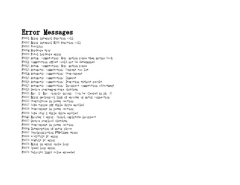
Error MessagesF9001 Error internal function call.F9002 Error internal RTOS function callF9003 WatchdogF9004 Hardware trapF8000 Fatal hardware errorF8010 Autom. commutation: Max. motion range when moving back F8011 Commutation offset could not be determinedF8012 Autom. commutation: Max. motion rangeF8013 Automatic commutation: Current too lowF8014 Automatic commutation: OvercurrentF8015 Automatic commutation: TimeoutF8016 Automatic commutation: Iteration without resultF8017 Automatic commutation: Incorrect commutation adjustment F8018 Device overtemperature shutdownF8022 Enc. 1: Enc. signals incorr. (can be cleared in ph. 2) F8023 Error mechanical link of encoder or motor connectionF8025 Overvoltage in power sectionF8027 Safe torque off while drive enabledF8028 Overcurrent in power sectionF8030 Safe stop 1 while drive enabledF8042 Encoder 2 error: Signal amplitude incorrectF8057 Device overload shutdownF8060 Overcurrent in power sectionF8064 Interruption of motor phaseF8067 Synchronization PWM-Timer wrongF8069 +/-15Volt DC errorF8070 +24Volt DC errorF8076 Error in error angle loopF8078 Speed loop error.F8079 Velocity limit value exceededF8091 Power section defectiveF8100 Error when initializing the parameter handlingF8102 Error when initializing power sectionF8118 Invalid power section/firmware combinationF8120 Invalid control section/firmware combinationF8122 Control section defectiveF8129 Incorrect optional module firmwareF8130 Firmware of option 2 of safety technology defectiveF8133 Error when checking interrupting circuitsF8134 SBS: Fatal errorF8135 SMD: Velocity exceededF8140 Fatal CCD error.F8201 Safety command for basic initialization incorrectF8203 Safety technology configuration parameter invalidF8813 Connection error mains chokeF8830 Power section errorF8838 Overcurrent external braking resistorF7010 Safely-limited increment exceededF7011 Safely-monitored position, exceeded in pos. DirectionF7012 Safely-monitored position, exceeded in neg. DirectionF7013 Safely-limited speed exceededF7020 Safe maximum speed exceededF7021 Safely-limited position exceededF7030 Position window Safe stop 2 exceededF7031 Incorrect direction of motionF7040 Validation error parameterized - effective thresholdF7041 Actual position value validation errorF7042 Validation error of safe operation modeF7043 Error of output stage interlockF7050 Time for stopping process exceeded8.3.15 F7051 Safely-monitored deceleration exceeded (159)8.4 Travel Range Errors (F6xxx) (161)8.4.1 Behavior in the Case of Travel Range Errors (161)8.4.2 F6010 PLC Runtime Error (162)8.4.3 F6024 Maximum braking time exceeded (163)8.4.4 F6028 Position limit value exceeded (overflow) (164)8.4.5 F6029 Positive position limit exceeded (164)8.4.6 F6030 Negative position limit exceeded (165)8.4.7 F6034 Emergency-Stop (166)8.4.8 F6042 Both travel range limit switches activated (167)8.4.9 F6043 Positive travel range limit switch activated (167)8.4.10 F6044 Negative travel range limit switch activated (168)8.4.11 F6140 CCD slave error (emergency halt) (169)8.5 Interface Errors (F4xxx) (169)8.5.1 Behavior in the Case of Interface Errors (169)8.5.2 F4001 Sync telegram failure (170)8.5.3 F4002 RTD telegram failure (171)8.5.4 F4003 Invalid communication phase shutdown (172)8.5.5 F4004 Error during phase progression (172)8.5.6 F4005 Error during phase regression (173)8.5.7 F4006 Phase switching without ready signal (173)8.5.8 F4009 Bus failure (173)8.5.9 F4012 Incorrect I/O length (175)8.5.10 F4016 PLC double real-time channel failure (176)8.5.11 F4017 S-III: Incorrect sequence during phase switch (176)8.5.12 F4034 Emergency-Stop (177)8.5.13 F4140 CCD communication error (178)8.6 Non-Fatal Safety Technology Errors (F3xxx) (178)8.6.1 Behavior in the Case of Non-Fatal Safety Technology Errors (178)8.6.2 F3111 Refer. missing when selecting safety related end pos (179)8.6.3 F3112 Safe reference missing (179)8.6.4 F3115 Brake check time interval exceeded (181)Troubleshooting Guide | Rexroth IndraDrive Electric Drivesand ControlsI Bosch Rexroth AG VII/XXIITable of ContentsPage8.6.5 F3116 Nominal load torque of holding system exceeded (182)8.6.6 F3117 Actual position values validation error (182)8.6.7 F3122 SBS: System error (183)8.6.8 F3123 SBS: Brake check missing (184)8.6.9 F3130 Error when checking input signals (185)8.6.10 F3131 Error when checking acknowledgment signal (185)8.6.11 F3132 Error when checking diagnostic output signal (186)8.6.12 F3133 Error when checking interrupting circuits (187)8.6.13 F3134 Dynamization time interval incorrect (188)8.6.14 F3135 Dynamization pulse width incorrect (189)8.6.15 F3140 Safety parameters validation error (192)8.6.16 F3141 Selection validation error (192)8.6.17 F3142 Activation time of enabling control exceeded (193)8.6.18 F3143 Safety command for clearing errors incorrect (194)8.6.19 F3144 Incorrect safety configuration (195)8.6.20 F3145 Error when unlocking the safety door (196)8.6.21 F3146 System error channel 2 (197)8.6.22 F3147 System error channel 1 (198)8.6.23 F3150 Safety command for system start incorrect (199)8.6.24 F3151 Safety command for system halt incorrect (200)8.6.25 F3152 Incorrect backup of safety technology data (201)8.6.26 F3160 Communication error of safe communication (202)8.7 Non-Fatal Errors (F2xxx) (202)8.7.1 Behavior in the Case of Non-Fatal Errors (202)8.7.2 F2002 Encoder assignment not allowed for synchronization (203)8.7.3 F2003 Motion step skipped (203)8.7.4 F2004 Error in MotionProfile (204)8.7.5 F2005 Cam table invalid (205)8.7.6 F2006 MMC was removed (206)8.7.7 F2007 Switching to non-initialized operation mode (206)8.7.8 F2008 RL The motor type has changed (207)8.7.9 F2009 PL Load parameter default values (208)8.7.10 F2010 Error when initializing digital I/O (-> S-0-0423) (209)8.7.11 F2011 PLC - Error no. 1 (210)8.7.12 F2012 PLC - Error no. 2 (210)8.7.13 F2013 PLC - Error no. 3 (211)8.7.14 F2014 PLC - Error no. 4 (211)8.7.15 F2018 Device overtemperature shutdown (211)8.7.16 F2019 Motor overtemperature shutdown (212)8.7.17 F2021 Motor temperature monitor defective (213)8.7.18 F2022 Device temperature monitor defective (214)8.7.19 F2025 Drive not ready for control (214)8.7.20 F2026 Undervoltage in power section (215)8.7.21 F2027 Excessive oscillation in DC bus (216)8.7.22 F2028 Excessive deviation (216)8.7.23 F2031 Encoder 1 error: Signal amplitude incorrect (217)VIII/XXII Bosch Rexroth AG | Electric Drivesand ControlsRexroth IndraDrive | Troubleshooting GuideTable of ContentsPage8.7.24 F2032 Validation error during commutation fine adjustment (217)8.7.25 F2033 External power supply X10 error (218)8.7.26 F2036 Excessive position feedback difference (219)8.7.27 F2037 Excessive position command difference (220)8.7.28 F2039 Maximum acceleration exceeded (220)8.7.29 F2040 Device overtemperature 2 shutdown (221)8.7.30 F2042 Encoder 2: Encoder signals incorrect (222)8.7.31 F2043 Measuring encoder: Encoder signals incorrect (222)8.7.32 F2044 External power supply X15 error (223)8.7.33 F2048 Low battery voltage (224)8.7.34 F2050 Overflow of target position preset memory (225)8.7.35 F2051 No sequential block in target position preset memory (225)8.7.36 F2053 Incr. encoder emulator: Pulse frequency too high (226)8.7.37 F2054 Incr. encoder emulator: Hardware error (226)8.7.38 F2055 External power supply dig. I/O error (227)8.7.39 F2057 Target position out of travel range (227)8.7.40 F2058 Internal overflow by positioning input (228)8.7.41 F2059 Incorrect command value direction when positioning (229)8.7.42 F2063 Internal overflow master axis generator (230)8.7.43 F2064 Incorrect cmd value direction master axis generator (230)8.7.44 F2067 Synchronization to master communication incorrect (231)8.7.45 F2068 Brake error (231)8.7.46 F2069 Error when releasing the motor holding brake (232)8.7.47 F2074 Actual pos. value 1 outside absolute encoder window (232)8.7.48 F2075 Actual pos. value 2 outside absolute encoder window (233)8.7.49 F2076 Actual pos. value 3 outside absolute encoder window (234)8.7.50 F2077 Current measurement trim wrong (235)8.7.51 F2086 Error supply module (236)8.7.52 F2087 Module group communication error (236)8.7.53 F2100 Incorrect access to command value memory (237)8.7.54 F2101 It was impossible to address MMC (237)8.7.55 F2102 It was impossible to address I2C memory (238)8.7.56 F2103 It was impossible to address EnDat memory (238)8.7.57 F2104 Commutation offset invalid (239)8.7.58 F2105 It was impossible to address Hiperface memory (239)8.7.59 F2110 Error in non-cyclical data communic. of power section (240)8.7.60 F2120 MMC: Defective or missing, replace (240)8.7.61 F2121 MMC: Incorrect data or file, create correctly (241)8.7.62 F2122 MMC: Incorrect IBF file, correct it (241)8.7.63 F2123 Retain data backup impossible (242)8.7.64 F2124 MMC: Saving too slowly, replace (243)8.7.65 F2130 Error comfort control panel (243)8.7.66 F2140 CCD slave error (243)8.7.67 F2150 MLD motion function block error (244)8.7.68 F2174 Loss of motor encoder reference (244)8.7.69 F2175 Loss of optional encoder reference (245)Troubleshooting Guide | Rexroth IndraDrive Electric Drivesand Controls| Bosch Rexroth AG IX/XXIITable of ContentsPage8.7.70 F2176 Loss of measuring encoder reference (246)8.7.71 F2177 Modulo limitation error of motor encoder (246)8.7.72 F2178 Modulo limitation error of optional encoder (247)8.7.73 F2179 Modulo limitation error of measuring encoder (247)8.7.74 F2190 Incorrect Ethernet configuration (248)8.7.75 F2260 Command current limit shutoff (249)8.7.76 F2270 Analog input 1 or 2, wire break (249)8.7.77 F2802 PLL is not synchronized (250)8.7.78 F2814 Undervoltage in mains (250)8.7.79 F2815 Overvoltage in mains (251)8.7.80 F2816 Softstart fault power supply unit (251)8.7.81 F2817 Overvoltage in power section (251)8.7.82 F2818 Phase failure (252)8.7.83 F2819 Mains failure (253)8.7.84 F2820 Braking resistor overload (253)8.7.85 F2821 Error in control of braking resistor (254)8.7.86 F2825 Switch-on threshold braking resistor too low (255)8.7.87 F2833 Ground fault in motor line (255)8.7.88 F2834 Contactor control error (256)8.7.89 F2835 Mains contactor wiring error (256)8.7.90 F2836 DC bus balancing monitor error (257)8.7.91 F2837 Contactor monitoring error (257)8.7.92 F2840 Error supply shutdown (257)8.7.93 F2860 Overcurrent in mains-side power section (258)8.7.94 F2890 Invalid device code (259)8.7.95 F2891 Incorrect interrupt timing (259)8.7.96 F2892 Hardware variant not supported (259)8.8 SERCOS Error Codes / Error Messages of Serial Communication (259)9 Warnings (Exxxx) (263)9.1 Fatal Warnings (E8xxx) (263)9.1.1 Behavior in the Case of Fatal Warnings (263)9.1.2 E8025 Overvoltage in power section (263)9.1.3 E8026 Undervoltage in power section (264)9.1.4 E8027 Safe torque off while drive enabled (265)9.1.5 E8028 Overcurrent in power section (265)9.1.6 E8029 Positive position limit exceeded (266)9.1.7 E8030 Negative position limit exceeded (267)9.1.8 E8034 Emergency-Stop (268)9.1.9 E8040 Torque/force actual value limit active (268)9.1.10 E8041 Current limit active (269)9.1.11 E8042 Both travel range limit switches activated (269)9.1.12 E8043 Positive travel range limit switch activated (270)9.1.13 E8044 Negative travel range limit switch activated (271)9.1.14 E8055 Motor overload, current limit active (271)9.1.15 E8057 Device overload, current limit active (272)X/XXII Bosch Rexroth AG | Electric Drivesand ControlsRexroth IndraDrive | Troubleshooting GuideTable of ContentsPage9.1.16 E8058 Drive system not ready for operation (273)9.1.17 E8260 Torque/force command value limit active (273)9.1.18 E8802 PLL is not synchronized (274)9.1.19 E8814 Undervoltage in mains (275)9.1.20 E8815 Overvoltage in mains (275)9.1.21 E8818 Phase failure (276)9.1.22 E8819 Mains failure (276)9.2 Warnings of Category E4xxx (277)9.2.1 E4001 Double MST failure shutdown (277)9.2.2 E4002 Double MDT failure shutdown (278)9.2.3 E4005 No command value input via master communication (279)9.2.4 E4007 SERCOS III: Consumer connection failed (280)9.2.5 E4008 Invalid addressing command value data container A (280)9.2.6 E4009 Invalid addressing actual value data container A (281)9.2.7 E4010 Slave not scanned or address 0 (281)9.2.8 E4012 Maximum number of CCD slaves exceeded (282)9.2.9 E4013 Incorrect CCD addressing (282)9.2.10 E4014 Incorrect phase switch of CCD slaves (283)9.3 Possible Warnings When Operating Safety Technology (E3xxx) (283)9.3.1 Behavior in Case a Safety Technology Warning Occurs (283)9.3.2 E3100 Error when checking input signals (284)9.3.3 E3101 Error when checking acknowledgment signal (284)9.3.4 E3102 Actual position values validation error (285)9.3.5 E3103 Dynamization failed (285)9.3.6 E3104 Safety parameters validation error (286)9.3.7 E3105 Validation error of safe operation mode (286)9.3.8 E3106 System error safety technology (287)9.3.9 E3107 Safe reference missing (287)9.3.10 E3108 Safely-monitored deceleration exceeded (288)9.3.11 E3110 Time interval of forced dynamization exceeded (289)9.3.12 E3115 Prewarning, end of brake check time interval (289)9.3.13 E3116 Nominal load torque of holding system reached (290)9.4 Non-Fatal Warnings (E2xxx) (290)9.4.1 Behavior in Case a Non-Fatal Warning Occurs (290)9.4.2 E2010 Position control with encoder 2 not possible (291)9.4.3 E2011 PLC - Warning no. 1 (291)9.4.4 E2012 PLC - Warning no. 2 (291)9.4.5 E2013 PLC - Warning no. 3 (292)9.4.6 E2014 PLC - Warning no. 4 (292)9.4.7 E2021 Motor temperature outside of measuring range (292)9.4.8 E2026 Undervoltage in power section (293)9.4.9 E2040 Device overtemperature 2 prewarning (294)9.4.10 E2047 Interpolation velocity = 0 (294)9.4.11 E2048 Interpolation acceleration = 0 (295)9.4.12 E2049 Positioning velocity >= limit value (296)9.4.13 E2050 Device overtemp. Prewarning (297)Troubleshooting Guide | Rexroth IndraDrive Electric Drivesand Controls| Bosch Rexroth AG XI/XXIITable of ContentsPage9.4.14 E2051 Motor overtemp. prewarning (298)9.4.15 E2053 Target position out of travel range (298)9.4.16 E2054 Not homed (300)9.4.17 E2055 Feedrate override S-0-0108 = 0 (300)9.4.18 E2056 Torque limit = 0 (301)9.4.19 E2058 Selected positioning block has not been programmed (302)9.4.20 E2059 Velocity command value limit active (302)9.4.21 E2061 Device overload prewarning (303)9.4.22 E2063 Velocity command value > limit value (304)9.4.23 E2064 Target position out of num. range (304)9.4.24 E2069 Holding brake torque too low (305)9.4.25 E2070 Acceleration limit active (306)9.4.26 E2074 Encoder 1: Encoder signals disturbed (306)9.4.27 E2075 Encoder 2: Encoder signals disturbed (307)9.4.28 E2076 Measuring encoder: Encoder signals disturbed (308)9.4.29 E2077 Absolute encoder monitoring, motor encoder (encoder alarm) (308)9.4.30 E2078 Absolute encoder monitoring, opt. encoder (encoder alarm) (309)9.4.31 E2079 Absolute enc. monitoring, measuring encoder (encoder alarm) (309)9.4.32 E2086 Prewarning supply module overload (310)9.4.33 E2092 Internal synchronization defective (310)9.4.34 E2100 Positioning velocity of master axis generator too high (311)9.4.35 E2101 Acceleration of master axis generator is zero (312)9.4.36 E2140 CCD error at node (312)9.4.37 E2270 Analog input 1 or 2, wire break (312)9.4.38 E2802 HW control of braking resistor (313)9.4.39 E2810 Drive system not ready for operation (314)9.4.40 E2814 Undervoltage in mains (314)9.4.41 E2816 Undervoltage in power section (314)9.4.42 E2818 Phase failure (315)9.4.43 E2819 Mains failure (315)9.4.44 E2820 Braking resistor overload prewarning (316)9.4.45 E2829 Not ready for power on (316)。

JOINT INDUSTRY STANDARDAcoustic Microscopy for Non-HermeticEncapsulatedElectronicComponents IPC/JEDEC J-STD-035APRIL1999Supersedes IPC-SM-786 Supersedes IPC-TM-650,2.6.22Notice EIA/JEDEC and IPC Standards and Publications are designed to serve thepublic interest through eliminating misunderstandings between manufacturersand purchasers,facilitating interchangeability and improvement of products,and assisting the purchaser in selecting and obtaining with minimum delaythe proper product for his particular need.Existence of such Standards andPublications shall not in any respect preclude any member or nonmember ofEIA/JEDEC or IPC from manufacturing or selling products not conformingto such Standards and Publications,nor shall the existence of such Standardsand Publications preclude their voluntary use by those other than EIA/JEDECand IPC members,whether the standard is to be used either domestically orinternationally.Recommended Standards and Publications are adopted by EIA/JEDEC andIPC without regard to whether their adoption may involve patents on articles,materials,or processes.By such action,EIA/JEDEC and IPC do not assumeany liability to any patent owner,nor do they assume any obligation whateverto parties adopting the Recommended Standard or ers are alsowholly responsible for protecting themselves against all claims of liabilities forpatent infringement.The material in this joint standard was developed by the EIA/JEDEC JC-14.1Committee on Reliability Test Methods for Packaged Devices and the IPCPlastic Chip Carrier Cracking Task Group(B-10a)The J-STD-035supersedes IPC-TM-650,Test Method2.6.22.For Technical Information Contact:Electronic Industries Alliance/ JEDEC(Joint Electron Device Engineering Council)2500Wilson Boulevard Arlington,V A22201Phone(703)907-7560Fax(703)907-7501IPC2215Sanders Road Northbrook,IL60062-6135 Phone(847)509-9700Fax(847)509-9798Please use the Standard Improvement Form shown at the end of thisdocument.©Copyright1999.The Electronic Industries Alliance,Arlington,Virginia,and IPC,Northbrook,Illinois.All rights reserved under both international and Pan-American copyright conventions.Any copying,scanning or other reproduction of these materials without the prior written consent of the copyright holder is strictly prohibited and constitutes infringement under the Copyright Law of the United States.IPC/JEDEC J-STD-035Acoustic Microscopyfor Non-Hermetic EncapsulatedElectronicComponentsA joint standard developed by the EIA/JEDEC JC-14.1Committee on Reliability Test Methods for Packaged Devices and the B-10a Plastic Chip Carrier Cracking Task Group of IPCUsers of this standard are encouraged to participate in the development of future revisions.Contact:EIA/JEDEC Engineering Department 2500Wilson Boulevard Arlington,V A22201 Phone(703)907-7500 Fax(703)907-7501IPC2215Sanders Road Northbrook,IL60062-6135 Phone(847)509-9700Fax(847)509-9798ASSOCIATION CONNECTINGELECTRONICS INDUSTRIESAcknowledgmentMembers of the Joint IPC-EIA/JEDEC Moisture Classification Task Group have worked to develop this document.We would like to thank them for their dedication to this effort.Any Standard involving a complex technology draws material from a vast number of sources.While the principal members of the Joint Moisture Classification Working Group are shown below,it is not possible to include all of those who assisted in the evolution of this Standard.To each of them,the mem-bers of the EIA/JEDEC and IPC extend their gratitude.IPC Packaged Electronic Components Committee ChairmanMartin FreedmanAMP,Inc.IPC Plastic Chip Carrier Cracking Task Group,B-10a ChairmanSteven MartellSonoscan,Inc.EIA/JEDEC JC14.1CommitteeChairmanJack McCullenIntel Corp.EIA/JEDEC JC14ChairmanNick LycoudesMotorolaJoint Working Group MembersCharlie Baker,TIChristopher Brigham,Hi/FnRalph Carbone,Hewlett Packard Co. Don Denton,TIMatt Dotty,AmkorMichele J.DiFranza,The Mitre Corp. Leo Feinstein,Allegro Microsystems Inc.Barry Fernelius,Hewlett Packard Co. Chris Fortunko,National Institute of StandardsRobert J.Gregory,CAE Electronics, Inc.Curtis Grosskopf,IBM Corp.Bill Guthrie,IBM Corp.Phil Johnson,Philips Semiconductors Nick Lycoudes,MotorolaSteven R.Martell,Sonoscan Inc. Jack McCullen,Intel Corp.Tom Moore,TIDavid Nicol,Lucent Technologies Inc.Pramod Patel,Advanced Micro Devices Inc.Ramon R.Reglos,XilinxCorazon Reglos,AdaptecGerald Servais,Delphi Delco Electronics SystemsRichard Shook,Lucent Technologies Inc.E.Lon Smith,Lucent Technologies Inc.Randy Walberg,NationalSemiconductor Corp.Charlie Wu,AdaptecEdward Masami Aoki,HewlettPackard LaboratoriesFonda B.Wu,Raytheon Systems Co.Richard W.Boerdner,EJE ResearchVictor J.Brzozowski,NorthropGrumman ES&SDMacushla Chen,Wus Printed CircuitCo.Ltd.Jeffrey C.Colish,Northrop GrummanCorp.Samuel J.Croce,Litton AeroProducts DivisionDerek D-Andrade,Surface MountTechnology CentreRao B.Dayaneni,Hewlett PackardLaboratoriesRodney Dehne,OEM WorldwideJames F.Maguire,Boeing Defense&Space GroupKim Finch,Boeing Defense&SpaceGroupAlelie Funcell,Xilinx Inc.Constantino J.Gonzalez,ACMEMunir Haq,Advanced Micro DevicesInc.Larry A.Hargreaves,DC.ScientificInc.John T.Hoback,Amoco ChemicalCo.Terence Kern,Axiom Electronics Inc.Connie M.Korth,K-Byte/HibbingManufacturingGabriele Marcantonio,NORTELCharles Martin,Hewlett PackardLaboratoriesRichard W.Max,Alcatel NetworkSystems Inc.Patrick McCluskey,University ofMarylandJames H.Moffitt,Moffitt ConsultingServicesRobert Mulligan,Motorola Inc.James E.Mumby,CibaJohn Northrup,Lockheed MartinCorp.Dominique K.Numakura,LitchfieldPrecision ComponentsNitin B.Parekh,Unisys Corp.Bella Poborets,Lucent TechnologiesInc.D.Elaine Pope,Intel Corp.Ray Prasad,Ray Prasad ConsultancyGroupAlbert Puah,Adaptec Inc.William Sepp,Technic Inc.Ralph W.Taylor,Lockheed MartinCorp.Ed R.Tidwell,DSC CommunicationsCorp.Nick Virmani,Naval Research LabKen Warren,Corlund ElectronicsCorp.Yulia B.Zaks,Lucent TechnologiesInc.IPC/JEDEC J-STD-035April1999 iiTable of Contents1SCOPE (1)2DEFINITIONS (1)2.1A-mode (1)2.2B-mode (1)2.3Back-Side Substrate View Area (1)2.4C-mode (1)2.5Through Transmission Mode (2)2.6Die Attach View Area (2)2.7Die Surface View Area (2)2.8Focal Length(FL) (2)2.9Focus Plane (2)2.10Leadframe(L/F)View Area (2)2.11Reflective Acoustic Microscope (2)2.12Through Transmission Acoustic Microscope (2)2.13Time-of-Flight(TOF) (3)2.14Top-Side Die Attach Substrate View Area (3)3APPARATUS (3)3.1Reflective Acoustic Microscope System (3)3.2Through Transmission AcousticMicroscope System (4)4PROCEDURE (4)4.1Equipment Setup (4)4.2Perform Acoustic Scans..........................................4Appendix A Acoustic Microscopy Defect CheckSheet (6)Appendix B Potential Image Pitfalls (9)Appendix C Some Limitations of AcousticMicroscopy (10)Appendix D Reference Procedure for PresentingApplicable Scanned Data (11)FiguresFigure1Example of A-mode Display (1)Figure2Example of B-mode Display (1)Figure3Example of C-mode Display (2)Figure4Example of Through Transmission Display (2)Figure5Diagram of a Reflective Acoustic MicroscopeSystem (3)Figure6Diagram of a Through Transmission AcousticMicroscope System (3)April1999IPC/JEDEC J-STD-035iiiIPC/JEDEC J-STD-035April1999This Page Intentionally Left BlankivApril1999IPC/JEDEC J-STD-035 Acoustic Microscopy for Non-Hermetic EncapsulatedElectronic Components1SCOPEThis test method defines the procedures for performing acoustic microscopy on non-hermetic encapsulated electronic com-ponents.This method provides users with an acoustic microscopy processflow for detecting defects non-destructively in plastic packages while achieving reproducibility.2DEFINITIONS2.1A-mode Acoustic data collected at the smallest X-Y-Z region defined by the limitations of the given acoustic micro-scope.An A-mode display contains amplitude and phase/polarity information as a function of time offlight at a single point in the X-Y plane.See Figure1-Example of A-mode Display.IPC-035-1 Figure1Example of A-mode Display2.2B-mode Acoustic data collected along an X-Z or Y-Z plane versus depth using a reflective acoustic microscope.A B-mode scan contains amplitude and phase/polarity information as a function of time offlight at each point along the scan line.A B-mode scan furnishes a two-dimensional(cross-sectional)description along a scan line(X or Y).See Figure2-Example of B-mode Display.IPC-035-2 Figure2Example of B-mode Display(bottom half of picture on left)2.3Back-Side Substrate View Area(Refer to Appendix A,Type IV)The interface between the encapsulant and the back of the substrate within the outer edges of the substrate surface.2.4C-mode Acoustic data collected in an X-Y plane at depth(Z)using a reflective acoustic microscope.A C-mode scan contains amplitude and phase/polarity information at each point in the scan plane.A C-mode scan furnishes a two-dimensional(area)image of echoes arising from reflections at a particular depth(Z).See Figure3-Example of C-mode Display.1IPC/JEDEC J-STD-035April1999IPC-035-3 Figure3Example of C-mode Display2.5Through Transmission Mode Acoustic data collected in an X-Y plane throughout the depth(Z)using a through trans-mission acoustic microscope.A Through Transmission mode scan contains only amplitude information at each point in the scan plane.A Through Transmission scan furnishes a two-dimensional(area)image of transmitted ultrasound through the complete thickness/depth(Z)of the sample/component.See Figure4-Example of Through Transmission Display.IPC-035-4 Figure4Example of Through Transmission Display2.6Die Attach View Area(Refer to Appendix A,Type II)The interface between the die and the die attach adhesive and/or the die attach adhesive and the die attach substrate.2.7Die Surface View Area(Refer to Appendix A,Type I)The interface between the encapsulant and the active side of the die.2.8Focal Length(FL)The distance in water at which a transducer’s spot size is at a minimum.2.9Focus Plane The X-Y plane at a depth(Z),which the amplitude of the acoustic signal is maximized.2.10Leadframe(L/F)View Area(Refer to Appendix A,Type V)The imaged area which extends from the outer L/F edges of the package to the L/F‘‘tips’’(wedge bond/stitch bond region of the innermost portion of the L/F.)2.11Reflective Acoustic Microscope An acoustic microscope that uses one transducer as both the pulser and receiver. (This is also known as a pulse/echo system.)See Figure5-Diagram of a Reflective Acoustic Microscope System.2.12Through Transmission Acoustic Microscope An acoustic microscope that transmits ultrasound completely through the sample from a sending transducer to a receiver on the opposite side.See Figure6-Diagram of a Through Transmis-sion Acoustic Microscope System.2April1999IPC/JEDEC J-STD-0353IPC/JEDEC J-STD-035April1999 3.1.6A broad band acoustic transducer with a center frequency in the range of10to200MHz for subsurface imaging.3.2Through Transmission Acoustic Microscope System(see Figure6)comprised of:3.2.1Items3.1.1to3.1.6above3.2.2Ultrasonic pulser(can be a pulser/receiver as in3.1.1)3.2.3Separate receiving transducer or ultrasonic detection system3.3Reference packages or standards,including packages with delamination and packages without delamination,for use during equipment setup.3.4Sample holder for pre-positioning samples.The holder should keep the samples from moving during the scan and maintain planarity.4PROCEDUREThis procedure is generic to all acoustic microscopes.For operational details related to this procedure that apply to a spe-cific model of acoustic microscope,consult the manufacturer’s operational manual.4.1Equipment Setup4.1.1Select the transducer with the highest useable ultrasonic frequency,subject to the limitations imposed by the media thickness and acoustic characteristics,package configuration,and transducer availability,to analyze the interfaces of inter-est.The transducer selected should have a low enough frequency to provide a clear signal from the interface of interest.The transducer should have a high enough frequency to delineate the interface of interest.Note:Through transmission mode may require a lower frequency and/or longer focal length than reflective mode.Through transmission is effective for the initial inspection of components to determine if defects are present.4.1.2Verify setup with the reference packages or standards(see3.3above)and settings that are appropriate for the trans-ducer chosen in4.1.1to ensure that the critical parameters at the interface of interest correlate to the reference standard uti-lized.4.1.3Place units in the sample holder in the coupling medium such that the upper surface of each unit is parallel with the scanning plane of the acoustic transducer.Sweep air bubbles away from the unit surface and from the bottom of the trans-ducer head.4.1.4At afixed distance(Z),align the transducer and/or stage for the maximum reflected amplitude from the top surface of the sample.The transducer must be perpendicular to the sample surface.4.1.5Focus by maximizing the amplitude,in the A-mode display,of the reflection from the interface designated for imag-ing.This is done by adjusting the Z-axis distance between the transducer and the sample.4.2Perform Acoustic Scans4.2.1Inspect the acoustic image(s)for any anomalies,verify that the anomaly is a package defect or an artifact of the imaging process,and record the results.(See Appendix A for an example of a check sheet that may be used.)To determine if an anomaly is a package defect or an artifact of the imaging process it is recommended to analyze the A-mode display at the location of the anomaly.4.2.2Consider potential pitfalls in image interpretation listed in,but not limited to,Appendix B and some of the limita-tions of acoustic microscopy listed in,but not limited to,Appendix C.If necessary,make adjustments to the equipment setup to optimize the results and rescan.4April1999IPC/JEDEC J-STD-035 4.2.3Evaluate the acoustic images using the failure criteria specified in other appropriate documents,such as J-STD-020.4.2.4Record the images and thefinal instrument setup parameters for documentation purposes.An example checklist is shown in Appendix D.5IPC/JEDEC J-STD-035April19996April1999IPC/JEDEC J-STD-035Appendix AAcoustic Microscopy Defect Check Sheet(continued)CIRCUIT SIDE SCANImage File Name/PathDelamination(Type I)Die Circuit Surface/Encapsulant Number Affected:Average%Location:Corner Edge Center (Type II)Die/Die Attach Number Affected:Average%Location:Corner Edge Center (Type III)Encapsulant/Substrate Number Affected:Average%Location:Corner Edge Center (Type V)Interconnect tip Number Affected:Average%Interconnect Number Affected:Max.%Length(Type VI)Intra-Laminate Number Affected:Average%Location:Corner Edge Center Comments:CracksAre cracks present:Yes NoIf yes:Do any cracks intersect:bond wire ball bond wedge bond tab bump tab leadDoes crack extend from leadfinger to any other internal feature:Yes NoDoes crack extend more than two-thirds the distance from any internal feature to the external surfaceof the package:Yes NoAdditional verification required:Yes NoComments:Mold Compound VoidsAre voids present:Yes NoIf yes:Approx.size Location(if multiple voids,use comment section)Do any voids intersect:bond wire ball bond wedge bond tab bump tab lead Additional verification required:Yes NoComments:7IPC/JEDEC J-STD-035April1999Appendix AAcoustic Microscopy Defect Check Sheet(continued)NON-CIRCUIT SIDE SCANImage File Name/PathDelamination(Type IV)Encapsulant/Substrate Number Affected:Average%Location:Corner Edge Center (Type II)Substrate/Die Attach Number Affected:Average%Location:Corner Edge Center (Type V)Interconnect Number Affected:Max.%LengthLocation:Corner Edge Center (Type VI)Intra-Laminate Number Affected:Average%Location:Corner Edge Center (Type VII)Heat Spreader Number Affected:Average%Location:Corner Edge Center Additional verification required:Yes NoComments:CracksAre cracks present:Yes NoIf yes:Does crack extend more than two-thirds the distance from any internal feature to the external surfaceof the package:Yes NoAdditional verification required:Yes NoComments:Mold Compound VoidsAre voids present:Yes NoIf yes:Approx.size Location(if multiple voids,use comment section)Additional verification required:Yes NoComments:8Appendix BPotential Image PitfallsOBSERV ATIONS CAUSES/COMMENTSUnexplained loss of front surface signal Gain setting too lowSymbolization on package surfaceEjector pin knockoutsPin1and other mold marksDust,air bubbles,fingerprints,residueScratches,scribe marks,pencil marksCambered package edgeUnexplained loss of subsurface signal Gain setting too lowTransducer frequency too highAcoustically absorbent(rubbery)fillerLarge mold compound voidsPorosity/high concentration of small voidsAngled cracks in package‘‘Dark line boundary’’(phase cancellation)Burned molding compound(ESD/EOS damage)False or spotty indication of delamination Low acoustic impedance coating(polyimide,gel)Focus errorIncorrect delamination gate setupMultilayer interference effectsFalse indication of adhesion Gain set too high(saturation)Incorrect delamination gate setupFocus errorOverlap of front surface and subsurface echoes(transducerfrequency too low)Fluidfilling delamination areasApparent voiding around die edge Reflection from wire loopsIncorrect setting of void gateGraded intensity Die tilt or lead frame deformation Sample tiltApril1999IPC/JEDEC J-STD-0359Appendix CSome Limitations of Acoustic MicroscopyAcoustic microscopy is an analytical technique that provides a non-destructive method for examining plastic encapsulated components for the existence of delaminations,cracks,and voids.This technique has limitations that include the following: LIMITATION REASONAcoustic microscopy has difficulty infinding small defects if the package is too thick.The ultrasonic signal becomes more attenuated as a function of two factors:the depth into the package and the transducer fre-quency.The greater the depth,the greater the attenuation.Simi-larly,the higher the transducer frequency,the greater the attenu-ation as a function of depth.There are limitations on the Z-axis(axial)resolu-tion.This is a function of the transducer frequency.The higher the transducer frequency,the better the resolution.However,the higher frequency signal becomes attenuated more quickly as a function of depth.There are limitations on the X-Y(lateral)resolu-tion.The X-Y(lateral)resolution is a function of a number of differ-ent variables including:•Transducer characteristics,including frequency,element diam-eter,and focal length•Absorption and scattering of acoustic waves as a function of the sample material•Electromechanical properties of the X-Y stageIrregularly shaped packages are difficult to analyze.The technique requires some kind offlat reference surface.Typically,the upper surface of the package or the die surfacecan be used as references.In some packages,cambered packageedges can cause difficulty in analyzing defects near the edgesand below their surfaces.Edge Effect The edges cause difficulty in analyzing defects near the edge ofany internal features.IPC/JEDEC J-STD-035April1999 10April1999IPC/JEDEC J-STD-035Appendix DReference Procedure for Presenting Applicable Scanned DataMost of the settings described may be captured as a default for the particular supplier/product with specific changes recorded on a sample or lot basis.Setup Configuration(Digital Setup File Name and Contents)Calibration Procedure and Calibration/Reference Standards usedTransducerManufacturerModelCenter frequencySerial numberElement diameterFocal length in waterScan SetupScan area(X-Y dimensions)Scan step sizeHorizontalVerticalDisplayed resolutionHorizontalVerticalScan speedPulser/Receiver SettingsGainBandwidthPulseEnergyRepetition rateReceiver attenuationDampingFilterEcho amplitudePulse Analyzer SettingsFront surface gate delay relative to trigger pulseSubsurface gate(if used)High passfilterDetection threshold for positive oscillation,negative oscillationA/D settingsSampling rateOffset settingPer Sample SettingsSample orientation(top or bottom(flipped)view and location of pin1or some other distinguishing characteristic) Focus(point,depth,interface)Reference planeNon-default parametersSample identification information to uniquely distinguish it from others in the same group11IPC/JEDEC J-STD-035April1999Appendix DReference Procedure for Presenting Applicable Scanned Data(continued) Reference Procedure for Presenting Scanned DataImagefile types and namesGray scale and color image legend definitionsSignificance of colorsIndications or definition of delaminationImage dimensionsDepth scale of TOFDeviation from true aspect ratioImage type:A-mode,B-mode,C-mode,TOF,Through TransmissionA-mode waveforms should be provided for points of interest,such as delaminated areas.In addition,an A-mode image should be provided for a bonded area as a control.12Standard Improvement FormIPC/JEDEC J-STD-035The purpose of this form is to provide the Technical Committee of IPC with input from the industry regarding usage of the subject standard.Individuals or companies are invited to submit comments to IPC.All comments will be collected and dispersed to the appropriate committee(s).If you can provide input,please complete this form and return to:IPC2215Sanders RoadNorthbrook,IL 60062-6135Fax 847509.97981.I recommend changes to the following:Requirement,paragraph number Test Method number,paragraph numberThe referenced paragraph number has proven to be:Unclear Too RigidInErrorOther2.Recommendations forcorrection:3.Other suggestions for document improvement:Submitted by:Name Telephone Company E-mailAddress City/State/ZipDate ASSOCIATION CONNECTING ELECTRONICS INDUSTRIESASSOCIATION CONNECTINGELECTRONICS INDUSTRIESISBN#1-580982-28-X2215 Sanders Road, Northbrook, IL 60062-6135Tel. 847.509.9700 Fax 847.509.9798。


基于非下采样Contourlet变换的红外图像非线性增强新方法郭珉;蒋爱民;曹美【期刊名称】《计算机与现代化》【年(卷),期】2017(000)003【摘要】针对红外图像存在对比度和分辩率低、噪声大的问题,提出一种基于非下采样Contourlet变换的夜间红外图像增强新算法.首先对实际采集的夜间红外图像进行非下采样Contourlet变换得到图像的高频系数和低频系数,对于高频系数采用自适应阈值法确定高频阈值,通过判断边缘信息对弱边缘和强边缘做不同的处理,提升图像的边缘信息,而低频系数采用改进的伽马变换进行非线性修正处理提升图像的对比度;最后经反变换得到增强后的图像.实验结果表明,提出的算法能有效抑制红外图像的噪声,提高图像的对比度信息,视觉效果良好.%Considering the problems that the low contrast and large noise are two main characteristics of infrared image, the infrared image enhancement method is presented in this paper, which is based on normal distribution characteristics and NSCT transform.First of all, image`s high frequency coefficients and low-frequency coefficients are got by the actual acquisition of nighttime infrared image nonsubsampled contourlet transform, for high frequency coefficients, the adaptive threshold method is used to determine the high frequency threshold.By judging the edge information, the weak edge and strong edge are made different processing to enhance the edge of the image information.The low frequency coefficients are made nonlinear correction by using theimproved Gamma transform to improve the contrast of the image.Finally, the enhanced image is obtained by inverse transform.The experimental results show that the proposed algorithm can effectively suppress the noise of infrared image, improve the image contrast information, and the visual effect is good.【总页数】4页(P76-79)【作者】郭珉;蒋爱民;曹美【作者单位】河海大学物联网工程学院,江苏常州 213022;河海大学物联网工程学院,江苏常州 213022;河海大学物联网工程学院,江苏常州 213022【正文语种】中文【中图分类】TP391.4【相关文献】1.一种基于图像融合的红外图像增强新方法 [J], 林晓春;李存志2.一种基于特征分类的红外图像自适应匹配增强的新方法 [J], 胡窦明;赵海生;李云川;潘超;柳继勇3.一种基于同态滤波的红外图像增强新方法 [J], 胡窦明;赵海生;李云川;潘超;柳继勇4.一种基于图像融合的红外图像增强新方法 [J], 林晓春;王艳5.基于奇异值分解和非下采样Contourlet变换的红外图像增强新算法 [J], 赵翱东;奚茂龙;叶茜因版权原因,仅展示原文概要,查看原文内容请购买。


低噪声放大器的设计-射频课程设计射频设计报告低噪声放大器的设计目录1 前言 ........................................................................... ........................................ 1 2 低噪声放大器的主要技术指标 (1)2.1 工作频率与带宽 ........................................................................... ......... 1 2.2 噪声系数 ........................................................................... ..................... 2 2.3 增益 ........................................................................... ............................. 2 2.4 放大器的稳定性 ........................................................................... ......... 3 2.5 输入阻抗匹配 ........................................................................... ............. 3 2.6 端口驻波比和反射损耗 (3)3 低噪声放大器的设计指标 ........................................................................... .... 4 4 设计方案 ........................................................................... .. (5)4.1 直流分析及偏置电路的设计 ................................................................ 5 4.2 稳定性分析 ........................................................................... ................. 7 4.3 匹配网络设计 ........................................................................... ............. 9 4.4 最大增益的输出匹配 ..........................................................................12 4.5 匹配网络的实现 ........................................................................... ....... 16 4.6 版图的设计 ........................................................................... ............... 17 5. 学习心得 ........................................................................... ............................. 23 参考文献............................................................................ . (24)1 前言低噪声放大器(low noise amplifier,LNA)是射频接收机前端的重要组成部分。

本科生毕业设计[论文] 高增益低噪声放大器(LNA)的设计院系专业班级姓名学号指导教师2017年1月13日华中科技大学IC课程设计(论文)学位论文原创性声明本人郑重声明:所呈交的论文是本人在导师的指导下独立进行研究所取得的研究成果。
除了文中特别加以标注引用的内容外,本论文不包括任何其他个人或集体已经发表或撰写的成果作品。
本人完全意识到本声明的法律后果由本人承担。
作者签名:2017 年 1 月13 日学位论文版权使用授权书本学位论文作者完全了解学校有关保障、使用学位论文的规定,同意学校保留并向有关学位论文管理部门或机构送交论文的复印件和电子版,允许论文被查阅和借阅。
本人授权省级优秀学士论文评选机构将本学位论文的全部或部分内容编入有关数据进行检索,可以采用影印、缩印或扫描等复制手段保存和汇编本学位论文。
本学位论文属于1、保密囗,在年解密后适用本授权书2、不保密囗。
(请在以上相应方框内打“√”)作者签名:2017 年 1 月13 日导师签名:2017 年 1 月13 日摘要低噪声放大器(Low Noise Amplifier,LNA)作为整个射频接收系统第一级,直接影响着整个系统的性能。
它的主要功能就是将从天线接收到的微弱信号进行放大,同时将其输出给后级的混频器,在这个过程中LNA引入信号中的噪声非常低,对信号进行初步的降噪处理,如果信号在通过LNA时引入的噪声较大或者没有将信号放大,那么其后的射频模块将无法对有用信号进行处理。
所以应用中的低噪声放大器必须具有最佳的噪声系数(NF),具有良好的线性度且对信号有一定的放大功能。
基于以上的研究背景,本文设计了一款高增益宽带低噪声放大器,详细的介绍了它的设计过程。
文章首先对宽带低噪声放大器进行了简单介绍,包括它的研究背景及国内外发展现状,接着介绍了在设计低噪声放大器中我们要注意的几个主要的参数,包括噪声、功率增益、输入匹配、线性度和S参数。
最后详细的介绍了我们的电路设计过程,包括一级和二级电路的选择以及其中一些工艺参数的设计,并给出了仿真结果,供大家分析和讨论。

上海交通大学工程硕士学位论文ABSTRACTThis paper introduces general development situation of the radarreceiver , general function situation and the developing direction of theLNA, also introduces the present technique condition of the LNA. Itanalyses the noise characteristic of the radar receiver ,a method ofrealizing the low noise design and the characteristic of the HEMT. Thispaper also presents the noise of amplifier , the nonlinear characteristic ,the basic theories and the design method of the LNA .KEY WORDS: ADS,noise characteristic, match network.上海交通大学学位论文原创性声明本人郑重声明:所呈交的学位论文,是本人在导师的指导下,独立进行研究工作所取得的成果。
除文中已经注明引用的内容外,本论文不包含任何其他个人或集体已经发表或撰写过的作品成果。
对本文的研究做出重要贡献的个人和集体,均已在文中以明确方式标明。
本人完全意识到本声明的法律结果由本人承担。
学位论文作者签名:刘喜明日期:年月日上海交通大学学位论文版权使用授权书本学位论文作者完全了解学校有关保留、使用学位论文的规定,同意学校保留并向国家有关部门或机构送交论文的复印件和电子版,允许论文被查阅和借阅。
本人授权上海交通大学可以将本学位论文的全部或部分内容编入有关数据库进行检索,可以采用影印、缩印或扫描等复制手段保存和汇编本学位论文。
