CPH5604中文资料
- 格式:pdf
- 大小:42.82 KB
- 文档页数:4
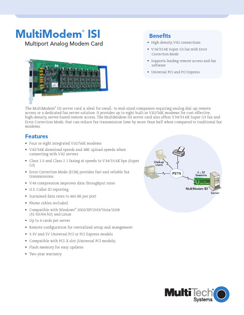
Multiport Analog Modem CardBenefits• High-density , V .92 connections • V .34/33.6K Super G3 fax with Error Correction Mode • Supports leading remote access and fax software • Universal PCI and PCI ExpressThe MultiModem ® ISI server card is ideal for small- to mid-sized companies requiring analog dial-up remote access or a dedicated fax server solution. It provides up to eight built-in V .92/56K modems for cost-effective,high-density , server-based remote access. The MultiModem ISI server card also offers V .34/33.6K Super G3 fax and Error Correction Mode, that can reduce fax transmission time by more than half when compared to traditional fax modems.Features• Four or eight integrated V .92/56K modems• V .92/56K download speeds and 48K upload speeds when connecting with V .92 servers • Class 1.0 and Class 2.1 faxing at speeds to V .34/33.6K bps (Super G3)• Error Correction Mode (ECM) provides fast and reliable fax transmissions • V .44 compression improves data throughput rates • U.S. Caller ID reporting• Sustained data rates to 460.8K per port • Phone cables included• Compatible with Windows ® 2000/XP/2003/Vista/2008 (32-bit/64-bit) and Linux • Up to 4 cards per server• Remote configuration for centralized setup and mangement • 3.3V and 5V Universal PCI or PCI Express models • Compatible with PCI-X slot (Universal PCI models)• Flash memory for easy updates • T wo-year warrantyMultiModem ®ISIWorld Headquarters Tel: (763) 785-3500 (800) EMEA Headquarters Multi-Tech Systems (EMEA)United KingdomTel: +(44) 118-959 7774Multi-Tech Systems (EMEA) FranceTel: +(33) 1 49 19 22 06HighlightsCost-Effective & Scalable. The MultiModem ISI server card provides four or eight dial-up sessions using only one server slot. When demand exceeds one modem card, you can simply add up to three additional cards.V.92 Dial-out Connections. The MultiModem ISI server card supports V .92/56K dial-out and V .34/33.6K dial-inconnections. With V .92 dial-out, you can achieve an upload speed of 48K bps (30% increase over V .90 modems).Enhanced Fax Features. The MultiModem ISI server card supports V .34 fax and Error Correction Mode providingsignificant performance and reliability enhancements over previous fax standards. V .34 sends and receives faxes at speeds up to 33.6K, more than double the speed of the V .17/14.4K fax standard. Error Correction Mode adds reliablility while increasing performance of faxtransmissions. Together these enhancements increase the performance of the MultiModem ISI server card to levels previously only found in more expensive dedicated fax boards and machines.V.44 Compression. V .44 compression standard improves V .42bis data compression anywhere from 20 to 60%, up to as much as 200% for certain types of highly compressible data. This compression technique enables data throughput rates of higher than 300K bps.Simplify Remote Access. The fully-integrated MultiModem ISI server card is easy to set up and manage. You only have to connect the phone lines. There are no external modems and power cords to hassle with; plus it saves back office space since the modems are on the prehensive Service and Support. The Multi-Techcommitment to service means we provide a two-year product warranty and service that includes free telephone technical support, 24-hour web site and ftp support.Ordering InformationProductDescriptionRegion ISI5634UPCI/8 V .92, 8-Modem Card - Universal PCI Global ISI5634UPCI/4 V .92, 4-Modem Card - Universal PCI Global ISI9234PCIE/8 V .92, 8-Modem Card - PCI Express Global ISI9234PCIE/4V .92, 4-Modem Card - PCI ExpressGlobalSpecificationsModemData: V .92, V .90, enhanced V .34, V .32bis, V .22bis Error Correction: V .42, MNP Class 3 & 4Data Compression: V .44, V .42bis, MNP Class 5FaxStandards: V .34, V .17, V .29, V .27ter, V .21, T.30, T.30Annex A, T.30 Annex F , T.31, T.31 Annex B, T.32 Annex C, TR29.2 Class 2 RecommendationRates: 33.6K, 31.2K, 28.8K, 26.4K, 24K, 21.6K, 19.2K, 16.8K, 14.4K, 12K, 9600, 7200, 4800, 2400, 300 bps Error Correction: ECMCompression: MH (T.4), MR (T.4), & MMR (T.6)Conversion: Real time (on-the-fly) compression conversionCommands: Class 1, 2, 1.0, 2.0, 2.1Bus Type3.3V & 5V Universal PCI or PCI Express (x1)Operating System SupportWindows 2000/XP/2003/Vista/2008 (32-bit/64-bit) & LinuxCablingFan out cable with 1 or 2 RJ45 connectors & 4 or 8 RJ11 connectorsPhysical DescriptionUniversal PCI Models:13.87" L × 4.97" W; 8.7 oz (35.2 cm × 12.6 cm; 247 g)PCI Express Models:13.87" L × 4.97" W; 8.5 oz (35.2 cm × 12.6 cm; 241 g)Operating EnvironmentTemperature Range: +23° to +140° F (-5° to +60° C)ApprovalsCE MarkEMC: FCC Part 15 Class B, EN 55022, EN 55024Safety: UL/cUL 60950-1, EN 60950-1, AS/NZS 60950:2000, CCCTelecom: 47CFR Part 68, CS03, TBR21Other countries also includedCopyright © 2008 by Multi-Tech Systems, Inc. All rights reserved.6/08 86000323Made in Mounds View, MN, U.S.A.Features and specifications are subject to change without notice.Trademarks / Registered Trademarks: MultiModem, Multi-Tech, and theMulti-Tech logo: Multi-Tech Systems, Inc. / All other products and technologies are the trademarks or registered trademarks of their respective holders.。

目录派克气动销售要约本文档中所述项目可由派克汉尼汾公司、其子公司或授权分销商销售。
此要约及其接受受本文件另一页中题为“销售要约”之条款的约束。
版权所有© 2020,2019派克汉尼汾公司。
保留所有权利P2H 网络节点P2M 网络节点非电路集成连接电路集成连接Turck 网络接口PCH 网络接口• 特性 .................................................................................3-6•电路集成连接 ...............................................................7-29 15407-2 - 尺寸 02, 01 (HB, HA) .....................................8-9 5599-2 - 尺寸 1, 2 (H1, H2) ........................................10-11 尺寸参数 ......................................................................12-21 5599-2 - 尺寸 3 (H3) ...................................................22-29•非电路集成连接 .........................................................30-51 15407-1 - 尺寸 02, 01 (HB, HA) ......................................31 5599-1 - 尺寸 1, 2 (H1, H2) ........................................32-35 订货信息 ......................................................................36-44 5599-1 - 尺寸 3 (H3) ...................................................45-51• 技术参数 / 附件 .........................................................52-66• 尺寸参数 ......................................................................67-77H 系列 ISO 阀网络通讯• 特性 .............................................................................78-89• P2M 网络节点 .............................................................90-97•P2H 网络节点............................................................98-102• PCH 网络接口 .........................................................103-119• H 系列网络接口......................................................120-134• Turck 网络接口 .......................................................135-154•附件 / 电缆..............................................................155-157•技术参数 / 尺寸参数 .............................................158-163H 系列 ISO 阀特性H 系列 ISO 阀H 系列ISO 阀符合国际标准15407和5599,为终端用户提供灵活的设置。


含氢硅烷偶联剂560资料表摘要:一、介绍含氢硅烷偶联剂5601.概述2.应用领域二、含氢硅烷偶联剂560 的性能特点1.化学结构2.物理性质3.反应特性三、含氢硅烷偶联剂560 的使用方法1.常规使用方法2.注意事项四、含氢硅烷偶联剂560 的应用实例1.环氧树脂应用2.玻纤增强应用五、总结正文:一、介绍含氢硅烷偶联剂560含氢硅烷偶联剂560 是一种硅烷偶联剂,具有特殊的化学结构和反应特性,被广泛应用于各种领域。
二、含氢硅烷偶联剂560 的性能特点1.化学结构含氢硅烷偶联剂560 的化学结构中,含有硅、氢、氧等元素,具有独特的分子结构。
2.物理性质含氢硅烷偶联剂560 通常为无色或淡黄色液体,具有较低的粘度,易于混合和施工。
3.反应特性含氢硅烷偶联剂560 具有较高的反应活性,在接触到固化剂时,可以迅速发生化学反应,形成稳定的化学键。
三、含氢硅烷偶联剂560 的使用方法1.常规使用方法含氢硅烷偶联剂560 通常与固化剂一起使用,在环氧树脂、玻纤增强等材料中起到偶联作用。
在使用过程中,需要确保含氢硅烷偶联剂560 与固化剂充分混合,以确保反应的顺利进行。
2.注意事项在使用含氢硅烷偶联剂560 时,需要注意避免与眼睛、皮肤等接触,以免造成刺激。
同时,应储存在阴凉、干燥的地方,防止阳光直射。
四、含氢硅烷偶联剂560 的应用实例1.环氧树脂应用含氢硅烷偶联剂560 可以用于环氧树脂的固化,提高环氧树脂的物理性能和耐候性。
2.玻纤增强应用含氢硅烷偶联剂560 可以用于玻纤增强材料,提高玻纤与基体的粘结力,从而提高材料的整体性能。
五、总结含氢硅烷偶联剂560 作为一种性能优异的偶联剂,在环氧树脂、玻纤增强等领域有着广泛的应用。

含氢硅烷偶联剂560资料表一、引言含氢硅烷偶联剂560是一种常用的功能性化学物质,用于改善聚合物与无机材料的粘附性能。
本文将详细探讨含氢硅烷偶联剂560的性质、应用领域以及合成方法等方面的相关内容。
二、含氢硅烷偶联剂560的性质2.1 物理性质•分子量:XXX•外观:XXX•溶解性:XXX•密度:XXX•熔点:XXX•沸点:XXX2.2 化学性质•搭接反应性:XXX•稳定性:XXX•酸碱性:XXX•氧化性:XXX•燃烧性:XXX三、含氢硅烷偶联剂560的应用领域3.1 聚合物改性1.增强聚合物与无机填料的粘附性;2.提高聚合物的力学性能;3.增加聚合物的热稳定性。
3.2 建筑材料1.用于改进水泥基复合材料的性能;2.用作水泥基、树脂基及硅酮等材料和无机表面的粘接促进剂。
3.3 电子材料1.作为导电胶黏剂的增粘剂;2.提高电子封装材料的耐热性和耐湿性。
3.4 涂料和油墨1.提高涂层和油墨的耐候性;2.提高涂层和油墨的附着力。
3.5 橡胶工业1.增强橡胶与无机催化剂的结合力;2.提高橡胶制品的机械性能和耐热性。
四、含氢硅烷偶联剂560的合成方法4.1 原料4.2 合成步骤1.步骤一:XXX2.步骤二:XXX3.步骤三:XXX4.3 反应机理4.4 优化条件和改进方法五、结论含氢硅烷偶联剂560作为一种功能性化学物质,在聚合物改性、建筑材料、电子材料、涂料和油墨、橡胶工业等领域都有重要的应用价值。
本文从物理性质、化学性质、应用领域和合成方法等多个方面对其进行了全面系统的探讨。
随着科学技术的进步和应用领域的扩大,含氢硅烷偶联剂560有望在更多的领域展现出广阔的应用前景。
六、参考文献[1] XXX [2] XXX [3] XXX。


COMPACT FLASH CARD CONNECTORS560H SERIES (CFA COMPATIBLE)s FEATURES•The connectors conform to the Compact Flash Association (CFA) specifications.•The terminal of the plug is a 0.635 mm pitch, one-row, SMT type.•Raised mounting type connectors (standoff), which allow mounting components under a connector, are also available.•The ejector mechanism makes insertion and ejection of a card easier is available.•There are two types of sockets for CFA cards: a straddle mount type and single-sided mounting type.s SPECIFICATIONSs PIN CONNECTOR (PLUG) CONTACT LENGTHsMATERIALSme t I la i r e t a M l a i r e t a m g n i t a l u s n I 0-V 49L U n i s e r S P P :y d ob n i a M 0-V 49L U T B P :e d i u G 0-V 49L U S B A :n o t t u B r o tc ud n o C y o l l a re p p o C gn i t a l P dl o g :t c a t n o C mu i d a l l a p :l a n i m r e T e p y T t c a t n o C .o n n i P h t g n e l t c a t n o C s n i p d n u o r g ,r e w o P 05,83,31,1).n i 691.0(m m 89.4s n i p n o i t c e d d r a C 62,52).n i 731.0(m m 84.3sn i p l a n g i s r e h t O re h t O ).n i 761.0(m m 42.4me t I no i t a c i f i c e p S e g n a r e r u t a r e p m e t g n i t a r e p O C °58+o t °55-t n e r r u c d e t a R C D A 5.0e g a t l o v d e t a R CA V 052e c n a t s i s e r t c a t n o C m 08Ω)A m 01,V m 02C D (x a m e c n a t s i s e r n o i t a l u s n I M 0001Ω,C D V 005,.n i m eg a t l o v d n a t s h t i w c i r t c e l e i D CD V 005RIGHT ANGLE PLUG, SMT TYPE (WITH NO EJECTOR)sDIMENSIONSs PC BOARD MOUNTING PATTERN (MOUNTING SIDE)s ORDERING PART NUMBER FCN-568H050-G/A1For above connector with ejector mechanism see page 3.Unit: mm (in.)Unit: mm (in.)40.16 (1.581)31.115±0.2 (1.225±.008)0.635±0.15(.025±.006)2x Ø2.2(.086)2x 4(0.157)2x2(0.079)35.9 (1.413)50.6 (1.992)16 (.630)19 (.749)25 (.984)26.5 (1.043)1(.039)4.5 (.177)4.5 (.177)1.25(.049)43.03±0.06 (1.225±.002)B30.48 (1.200)No. 13No. 381.27(.050)1.27(.050)1.4±0.05(.055±.002)No. 1No. 13BNo. 25No. 5040.16 (1.581)2x0.89±0.05(.035±.002)0.79±0.06 (.031±.002)1.75 (.069)2.6±0.03 (.102±.0001)2(.079)2.5 (0.098)5.25 (0.207)3.5 (0.138)4.5 (0.177)φ1.5+0 (0.059+0 )-0.1-0.004 3.5±08 (0.138±003)1(0.039)1 (.039)5.1(0.201)2.54 (0.1)1.8(.071)9.5 (0.374)11 (0.433)Section B-BRecommended PCB Pattern2 x 3(.079 x .118)46.13±0.15 (1.816±0.006)40.16±0.05 (1.581±0.002)31.115±0.05 (1.225±0.002)0.635±0.03 (0.025±0.001)2 × φ1.7±0.03(0.67±0.001)2 × φ2.2±0.05 (0.087±0.002)2±0.15(0.079±0.006)7.55±0.05(0.297±0.002)3.5±0.05(0.138±0.002)3±0.1 (.118±0.004)2 × 5±0.15(0.197±0.006)0.4±0.03 (0.016±0.001)No.38No.50No.26No.13No.1No.2547.10 -0 (1.854-0)7.45 (0.293)3.5 (0.138)5.55-0 (0.219-0)3 (.118)7.6-0(0.299-0)20.5-0(0.807-0)1.85-0.1 (0.073-0.004)+0+0The End of the P.C. BoardComponent mounting prohibited areaComponent mounting prohibited areas ORDERING PART NUMBER FOR CONNECTOR/EJECTOR KIT FCN-568H050-G/A1ACRIGHT ANGLE PLUG, SMT TYPE (WITH EJECTOR)sDIMENSIONSUnit: mm (in.)47.6 (1.874)23.8 (0.937)27.3 (1.074)5.5 (0.217)10.65 (0.420) a t c a r d e j e c t e d17.4 (0.685) a t c a r d i n s e r t e d6.75(0.266)29.25 (1.151)10.95 (0.431)28.6 (1.126)7.85 (0.309)0.3 (0.012)5.8 (0.228)1.5 (0.060)Connector/Ejector KitConnector/Ejector mechanism (P/N FCN-560HAC)RIGHT ANGLE PLUG, SMT TYPE (WITH NO EJECTOR, TO BE MOUNTED ON BACK OF PC BOARD)sDIMENSIONSs PC BOARD MOUNTING PATTERN (MOUNTING SIDE)s ORDERING PART NUMBER FCN-568H050-G/A2For above connector with ejector mechanism see page 5.Unit: mm (in.)Unit: mm (in.)40.16 (1.581)31.115±0.15 (1.225±0.006)0.635±0.15(0.025±0.006)2 x φ2.2(0.086)2 X 4(0.157)4.5(0.177)1 (0.039)1(0.039)16 (0.630)19 (0.749)25 (0.984)26.5 (1.043)1.25 (0.049)5.1 (0.201)2.5 (0.098)3.5±08 (0.138±003)5.25 (0.207)3.5 (0.138) 11 (0.433)φ1.50 (0.0590)000035.9 (1.413)2 x 0.89(0.035)50.6 (1.992)43.03±0.06 (1.225±0.002) 1.27(0.050)1.27 x (25-1) = 30.48 (1.200)No. 38No. 262 X 2.0 (0.079)40.16 (1.581)1.400(0.055000)BNo. 50No. 25No. 13 0.79 00(0.031000)No. 11.27 (0.050)4.5 (0.177)1.5(0.059)4.5 (0.177)2.54 (0.1)Section B-BB9.5(0.374) 1.8(0.070)No.13No.1No.25No.50No.38No.262±0.15(0.079±0.006)7.55±0.05 (0.297±0.002)3.5±0.05(0.138±0.002)0.4±0.03 (0.016±0.001)46.13±0.15 (1.816±0.006)0.635 × (50 – 1)= 31.115±0.05 (1.225±0.002)0.635±0.03(0.025±0.001)2 × φ1.7±0.03(0.67±0.001)2 × φ2.2±0.05(0.087±0.002)3±0.1(118±0.004)2 × 5±0.15(0.197±0.006)Recommended PCB pattern47.10 -0 (1.854-0)7.45 (0.293)3.5 (0.138)5.55 (0.219)3 (0.118) 7.6-0(0.299-0)20.5-0(0.807-0)1.85-0.1(0.073-0.004)+0+0The End of the P.C. BoardComponent mounting prohibited areaComponent mounting prohibited area2 x 3(.079 x .118)s ORDERING PART NUMBER FOR CONNECTOR/EJECTOR KIT FCN-568H050-G/A2ADRIGHT ANGLE PLUG, SMT TYPE (WITH EJECTOR, TO BE MOUNTED ON BACK OF PC BOARD)sDIMENSIONSUnit: mm (in.)47.6 (1.874)23.8 (0.937)27.3 (1.874)5.5 (0.217)10.65 (0.420) w h e n c a r d i s e j e c t e d17.4 (0.685)w h e n c a r d i s i n s e r t e d29.25 (1.151)10.95 (0.431)28.6 (1.126)0.3 (0.011)5.8 (0.228)1.5 (0.060)7.85 (0.309)Connector/Ejector KitConnector/Ejector mechanism (P/N FCN-560HAD)RIGHT-ANGLE PLUG, SMT TYPE (WITH NO EJECTOR, 1.64mm RAISED TYPE)sDIMENSIONSs PC BOARD MOUNTING PATTERN (MOUNTING SIDE)s ORDERING PART NUMBER FCN-568H050-G/A3For above connector with ejector mechanism see page 7.Unit: mm (in.)Unit: mm (in.)No.38No.50No.26No.1No.13No.252 × 3(0.079 x 0.118)2±0.15(0.079±0.006)7.55±0.05 (0.297±0.002)3.5±0.05(0.138±0.002)0.4±0.03 (0.016±0.001)46.13±0.15 (1.816±0.006)40.16±0.05 (1.581±0.002)0.635 × (50 – 1)= 31.115±0.05 (1.225±0.002)0.635±0.03 (0.025±0.001)2 × φ1.7±0.03(0.67±0.001)2 × φ2.2±0.05(0.087±0.002)3±0.1 (118±0.004)2 × 5±0.15(0.197±0.006)Recommended PCB patternComponent with 1.1 mm (0.043 in.)or less height can be mounted.47.10 -0 (1.854-0)7.45 (0.293)2.3(0.090)3.5 (0.138)5.55 (0.219)3 (0.118)7.6-0(0.299-0)20.5-0(0.807-0)3.0-0 (0.118-0)1.85-0.1 (0.073-0.004)+0+0The End of the P.C. BoardComponent mounting prohibited area Component mounting prohibited area50.60 (1.992)40.16 (1.581)31.115±0.15 (1.225±0.006)35.9 (1.413)2 x 0.89±0.05(0.035±0.002)2.0 (0.079)1.64 (0.065)2.5 (0.098)43.03±0.06 (1.225±0.002)0.635±0.15 (0.025±0.006)2 x φ2.2(0.086)2x 4(0.157)4.5(0.177)1 (0.039)16 (0.630)19 (0.749)25 (0.984)26.5 (1.043)4.5(0.177)5.25 (0.207)3.5(0.138)4.5 (0.177)11 (0.433)1.75 (0.069)1.27 (0.050)1.27(0.050)0.79 ±0.05(0.031±0.002) 1.4 ±0.05(0.055±0.002)φ1.5+0(0.059+0 )-0.1-0.004No. 1No. 26No. 38No. 13No. 25No. 503.5±08 (0.138±003)1(0.039)6.64 (0.261)BBASection B-B1.25 (0.050)2.54 (0.1)1.5 (0.060)9.5(0.374)1.8(0.070)30.48 (1.2)s ORDERING PART NUMBER FOR CONNECTOR/EJECTOR KIT FCN-568H050-G/A3ACRIGHT-ANGLE PLUG, SMT TYPE (WITH EJECTOR, 1.64mm (0.065 in.) RAISED TYPE)sDIMENSIONSUnit: mm (in.)1.84 (0.072)7.34 (0.289)Connector/Ejector Kit47.6 (1.874)23.8 (0.937)27.3 (1.074)5.5 (0.217)10.65 (0.420)w h e n c a r d i s e j e c t e d17.4 (0.685)w h e n c a r d i s i n s e r t e d6.75(0.266)28.6 (1.126)29.25 (1.151)4.05(0.159)1.5 (0.060)10.95 (0.431)7.85 (0.309)Connector/Ejector mechanism (P/N FCN-560HAC)RIGHT-ANGLE PLUG, SMT TYPE (WITH NO EJECTOR, 1.64mm (0.065) RAISED TYPE, TO BE MOUNTED ON BACK OF PC BOARD)s DIMENSIONSs ORDERING PART NUMBER FCN-568H050-G/A4For above connector with ejector mechanism see page 9.s ORDERING PART NUMBER FCN-568H050-G/A4ADRIGHT-ANGLE PLUG, SMT TYPE (WITH EJECTOR, 1.64mm (0.065 in.) RAISED TYPE, TO BE MOUNTED ON BACK OF PC BOARD)sDIMENSIONSUnit: mm (in.)6.75 (0.265)1.84 (0.072)7.34 (0.289)4.05 (0.159)Ejector mechanism (P/N FCN-560 HAD)Connector/Ejector Kit47.6 (1.874)23.8 (0.937)27.3 (1.074)5.5 (0.217)10.95 (0.431)7.85 (0.309)10.65 (0.420)w h e n c a r d i s e j e c t e d17.4 (0.685)w h e n c a r d i s i n s e r t e d29.95 (1.151)28.6 (1.126)1.5 (0.060)Part No: FCN-560HAC10.95 (0.431)5.5 (0.216)47.6 (1.874)23.8 (0.937)26.75 (1.053)5.5 (0.217)10.65 (0.420)w h e n c a r d i s e j e c t e d17.4 (0.685)w h e n c a r d i s i n s e r t e d28.6 (1.126)4.05(0.159)7.85 (0.309)29.25 (1.151)6.75 (0.266)FCN-560H Series Connector PLUG (Guide)Part No: FCN-560HAD10.95 (0.431)5.5(0.216)47.6 (1.874)23.8 (0.937)27.3 (1.075) 5.5 (0.217)10.65 (0.420)w h e n c a r d i s e j e c t e d17.4 (0.685)w h e n c a r d i s i n s e r t e d4.05(0.159)7.85 (0.309)29.25 (1.151)6.75 (0.266)28.6 (1.126)FCN-560 Series Connector PLUG (GUIDE)560H Series (Compact Flash Connector)11Dimensions are in millimeters (inches) Specifications subject to change© 2001 Fujitsu Components America, Inc. All company and product names are trademarks or registered trademarks of their respective owners. Rev. 09/2001JapanFujitsu Component Limited Gotanda-Chuo Building3-5, Higashigotanda 2-chome, Shinagawa-ku Tokyo 141, Japan Tel: (81-3) 5449-7010Fax: (81-3) 5449-2626Email:************** Web: North and South AmericaFujitsu Components America, Inc.250 E. Caribbean DriveSunnyvale, CA 94089 U.S.A.Tel: (1-408) 745-4900Fax: (1-408) 745-4970Email:*******************.com Web: EuropeFujitsu Components Europe B.V.Diamantlaan 252132 WV Hoofddorp NetherlandsTel: (31-23) 5560910Fax: (31-23) 5560950Email:***************************.com Web: Asia PacificFujitsu Components Asia Ltd.102E Pasir Panjang Road#04-01 Citilink Warehouse Complex Singapore 118529Tel: (65) 375-8560Fax: (65) 273-3021Email:*****************.com Fujitsu Components International Headquarter Offices。

元器件交易网IMPORTANT NOTICETexas Instruments and its subsidiaries (TI) reserve the right to make changes to their products or to discontinueany product or service without notice, and advise customers to obtain the latest version of relevant informationto verify, before placing orders, that information being relied on is current and complete. All products are soldsubject to the terms and conditions of sale supplied at the time of order acknowledgement, including thosepertaining to warranty, patent infringement, and limitation of liability.TI warrants performance of its semiconductor products to the specifications applicable at the time of sale inaccordance with TI’s standard warranty. Testing and other quality control techniques are utilized to the extentTI deems necessary to support this warranty. Specific testing of all parameters of each device is not necessarilyperformed, except those mandated by government requirements.CERTAIN APPLICATIONS USING SEMICONDUCTOR PRODUCTS MAY INVOLVE POTENTIAL RISKS OFDEATH, PERSONAL INJURY, OR SEVERE PROPERTY OR ENVIRONMENTAL DAMAGE (“CRITICALAPPLICATIONS”). TI SEMICONDUCTOR PRODUCTS ARE NOT DESIGNED, AUTHORIZED, ORWARRANTED TO BE SUITABLE FOR USE IN LIFE-SUPPORT DEVICES OR SYSTEMS OR OTHERCRITICAL APPLICATIONS. INCLUSION OF TI PRODUCTS IN SUCH APPLICATIONS IS UNDERSTOOD TOBE FULLY AT THE CUSTOMER’S RISK.In order to minimize risks associated with the customer’s applications, adequate design and operatingsafeguards must be provided by the customer to minimize inherent or procedural hazards.TI assumes no liability for applications assistance or customer product design. TI does not warrant or representthat any license, either express or implied, is granted under any patent right, copyright, mask work right, or otherintellectual property right of TI covering or relating to any combination, machine, or process in which suchsemiconductor products or services might be or are used. TI’s publication of information regarding any thirdparty’s products or services does not constitute TI’s approval, warranty or endorsement thereof.Copyright © 1999, Texas Instruments Incorporated。


PREPARED BY CHECKED BY APPROVED BYCustomer: TRANSFER MUL TISORT ELEKTRONIK SP .Z 0.0 Date: August 26, 2015SPECIFICATIONDescription: Aluminum Electrolytic Capacitors AISHI P/N: EPF2QM101W35OC SERIES: PFITEM: 330V100uF (Φ12.5X35) Customer P/N:No.: CRS-J-1508175APPROVED BYPlease Return One Copy with Your Approval承认后请寄回一份湖南艾华集团股份有限公司HUNAN AIHUA GROUP CO., L TDTel: (0737)6184466 Fax : (0737)6180493版本更改原因更改内容 生效日期CRS-J-1508175新建新建2015-8-26CustomerTRANSFER MUL TISORT ELEKTRONIK SP .Z 0.0SERIESPF DATE 2015-8-26FIG-1TABLE-1No.Customer Part No.Aishi Part No.Capacitance(uF)Tolerance on Rated Capacitance(%)Rated V oltage (Vdc)Operating Temp. Range(℃)tan δ (120Hz)(Max)Leakage Current (uA) (5min.)Endurance at 55℃(Hours)Dimensions (mm)Appearance Drawing No. D ΦL αd F F11 EPF2QM101W35OC 100 ±20 330 -25~+55 0.06 100 5000 12.53520.6 5.0/FIG-1F ±0.5PVCL+ α MAX 15 MIN4MIN¢d±0.05D+0.5 MAX1.概述SCOPE本承认书规定了PF 系列径向引线引出铝电解电容器的技术规范,本技术规范条文解释权归本公司所有。


Freescale Semiconductor MPC5604P Controller BoardUsers ManualOrder this document byMPC5604PCBUMRev. 0, 05/2009Table of ContentsIntroduction 61.1MPC5604P Controller Board Architecture . . . . . . . . . . . . . . . . . . . . . . . . . . . . . . . 61.2MPC5604P Controller Board Configuration Jumpers . . . . . . . . . . . . . . . . . . . . . . 71.3About this Manual . . . . . . . . . . . . . . . . . . . . . . . . . . . . . . . . . . . . . . . . . . . . . . . . 101.4Setup Guide . . . . . . . . . . . . . . . . . . . . . . . . . . . . . . . . . . . . . . . . . . . . . . . . . . . . . 11Operational Description 122.1Introduction . . . . . . . . . . . . . . . . . . . . . . . . . . . . . . . . . . . . . . . . . . . . . . . . . . . . . 122.2Electrical Characteristics . . . . . . . . . . . . . . . . . . . . . . . . . . . . . . . . . . . . . . . . . . . 13Pin Description 143.1Introduction . . . . . . . . . . . . . . . . . . . . . . . . . . . . . . . . . . . . . . . . . . . . . . . . . . . . . 143.2Signal Description . . . . . . . . . . . . . . . . . . . . . . . . . . . . . . . . . . . . . . . . . . . . . . . . 14Design Consideration 234.1Overview . . . . . . . . . . . . . . . . . . . . . . . . . . . . . . . . . . . . . . . . . . . . . . . . . . . . . . . 234.2MPC5604P . . . . . . . . . . . . . . . . . . . . . . . . . . . . . . . . . . . . . . . . . . . . . . . . . . . . . 234.3Clock Source . . . . . . . . . . . . . . . . . . . . . . . . . . . . . . . . . . . . . . . . . . . . . . . . . . . . 244.4UNI3 Interface and External Fault Management . . . . . . . . . . . . . . . . . . . . . . . . . 254.5Encoder Inputs . . . . . . . . . . . . . . . . . . . . . . . . . . . . . . . . . . . . . . . . . . . . . . . . . . 264.6Resolver and SINCOS Sensor . . . . . . . . . . . . . . . . . . . . . . . . . . . . . . . . . . . . . . 274.7Analog Signal Sensing . . . . . . . . . . . . . . . . . . . . . . . . . . . . . . . . . . . . . . . . . . . . 274.8Power Supplies and Voltage Reference . . . . . . . . . . . . . . . . . . . . . . . . . . . . . . . . 284.9UNI-3 PFC-PWM Signal (Power Factor Correction) . . . . . . . . . . . . . . . . . . . . . . 284.10UNI-3 Brake Signal . . . . . . . . . . . . . . . . . . . . . . . . . . . . . . . . . . . . . . . . . . . . . . . 294.11CAN and SafetyCAN Bus . . . . . . . . . . . . . . . . . . . . . . . . . . . . . . . . . . . . . . . . . . 294.12FlexRAY Interface . . . . . . . . . . . . . . . . . . . . . . . . . . . . . . . . . . . . . . . . . . . . . . . . 29MCPC5604P Controller Board Schematics 30Bill of Materials 42by: Petr KonvicnyFreescale SemiconductorCzech System CenterTo provide the most up-to-date information, the revision of our documents on the world-wide web will be the most current. Your printed copy may be an earlier revision. To verify that you have the latest information available, refer to .The following revision history table summarizes the changes contained in this document. For your convenience, the page number designators have been linked to the appropriate location.Revision HistoryTable0-1 Revision History TableDate RevisionlevelDescriptionPagenumber(s)6.3.20090Initial release N/ASection1. Introduction Freescale Semiconductor MPC5604P controller board is an embeded controller board integrated to Freescale Semiconductor embedded motion-control series of development tools. It provides controller functions for 3-phase BLDC, PMSM, and ACIM motors. It is supplied with a 40-pin ribbon cable interconnecting with, among others, one of the embedded motion-power stages or evaluation boards, providing a ready-made software-development platform for small permanent-magnet synchronous or brushless DC motors.The MPC5604P controller board is an evaluation-module type of board which includes an MPC5604P device, an encoder interface, resolver, sin/cos interface, communications options, digital and analog power supplies, and peripheral expansion connectors. The expansion connectors are intended for signal monitoring and user expandability. Test pads are provided for monitoring critical signals and voltage levels.1.1 MPC5604P Controller Board ArchitectureThe MPC5604P controller board facilitates the evaluation of various features present in the MPC5604P. It can be used to develop real-time software and hardware products based on MPC5604P. It provides the features neccesary for the user to write and debug software, demonstrate the functionality of that software, and to interface with the customer’s application specific device(s). The UNI-3 expansion connector enables this board to directly interface with the most of Freescale motor-control demo power stages. The MPC5604P controller board is flexible enough to allow the users to fully exploit the MPC5604P features to optimize the performance of their product, as shown in Figure1-1.Figure1-1 Controller Board Block Diagram1.2 MPC5604P Controller Board Configuration JumpersJumper groups and zero Ohm resistors1 shown in fig are used to configure various features on the MPC5604P controller board.1. Zero Ohm resistors are used instead of standard jumpers to minimize the distortion of analog signals, and to achieve a high signal-to-noise ratio.Table1-1 MPC5604P Controller Board Jumper Options#Selector Function Connections JP1,JP2CAN Terminate CAN bus node.closedJP104MC33905debug modeEnter SBC driver MC33905 to debug mode.closedJP105MC33905save modeEnter SBC driver MC33905 to safe mode.closedJP200Resolver Enable Resolver reference input signal from MCU disabled.open Resolver reference input signal from MCU enabled.closedJ203Resolver SINinputPositive input for SIN OPAM is DC offset voltage set up bytrimmer R209.1–2 Positive input for SIN OPAM is REFSIN input of resolver.2–3J204Resolver COSinputPositive input for COS OPAM is DC offset voltage set up bytrimmer R209.1–2 Positive input for COS OPAM is REFCOS input of resolver.2–3J205Phase Adigital signalResolver Phase A signal is connected to GPIO F[13].1–2SIN/COS Phase A signal is connected to GPIO F[13].2–3J206Phase Bdigital signalResolver Phase A signal is connected to GPIO A[5].1–2SIN/COS Phase A signal is connected to GPIO A[5].2–3J2Resolverinput signalResolver reference signal is generated by GPIO C[11].2–3Resolver reference signal is generated by GPIO C[12].1–2J301FAULT1selectionUNI-3 Phase A over-current signal is connected to FAULT1 inputG[9].1–2UNI-3 DC-bus over-current signal is connected to FAULT1 inputG[9].2–3J312BOOT selection MPC5604P boot from internal Flash.closedJ500Encoder 0Phase AEncoder0 JP500 pin three PHASE A input signal is connected toGPIO A[0].1–2 UNI-3 BEMFZCA input signal is connected to GPIO A[0].2–3J501Encoder 0Phase BEncoder0 JP500 pin four PHASE B input signal is connected toGPIO A[1].1–2 UNI-3 BEMFZCB input signal is connected to GPIO A[1].2–3J502Encoder 0IndexEncoder0 JP500 pin five INDEX input signal is connected toGPIO A[2].1–2 UNI-3 BEMFZCC input signal is connected to GPIO A[2].2–3J503Encoder 0HomeEncoder0 JP500 pin six HOME input signal is connected toGPIO A[3].closedDC BUS VoltageDC BSUS Voltage signal from UNI-3 is connected to GPIO B[13],ADC 1 input zero.R315populated DC BUSCurrentDC BUS Current signal from UNI-3 is connected to GPIO B[15],ADC 1 input two.R316populated Analog input 11UNI-3 Phase A current is connected to GPIO B[9], ADC 0/1 input11.R318populated UNI-3 Phase A Back-EMF Voltage is connected to GPIO B[9]mADC 0/1 input 11.R320populated Analog input 12UNI-3 Phase B current is connected to GPIO B[10], ADC 0/1input 12.R322populated UNI-3 Phase B Back-EMF Voltage is connected to GPIO B[10]mADC 0/1 input 12.R324populated Analog input 13UNI-3 Phase C current is connected to GPIO B[11], ADC 0/1input 13.R325populated UNI-3 Phase C Back-EMF Voltage is connected to GPIO B[11]mADC 0/1 input 13.R326populated TEMP UNI-3 Temperature signal is connected to ADC0 input zero.R328populated SERIAL UNI-3 Serial signal is connected to GPIO D[5].R330populated BRAKE UNI-3 Brake output signal is connected to GPIO C[3].R333populated PFC UNI-3 PFC output signal is connected to GPIO G[6] (PWMA3).R334populated PFC_EN UNI-3 PFC Enable signal is connected to GPIO G[7] (PWMB3).R335populated PFC_ZCUNI-3 PFC zero current signal is connected to GPIO G[5](PWMX3).R336populated Table1-1 MPC5604P Controller Board Jumper Options (Continued)#Selector Function ConnectionsFigure1-2 MPC5604P Controller Board1.3 About this ManualKey items can be found in the following locations in this manual:•Setup instructions are in 1.4 Setup Guide.•Pin assignments and a pin-by-pin description are shown in Section3. Pin Description.•Schematics and board circuitry description are found in Section4. Design Consideration.1.4 Setup GuideSetup and connections for the MPC5604P controller board are straightforward. The MPC5604P controller board connects to a Freescale Semiconductor embedded motion-control series power stage via 40-pin and 10-pin ribbon cables. The motor sensors like resolver, encoder, and so on plug into applicable connectors. Figure1-2 depicts a complete setup.Follow these steps to set up the board:1.Plug one end of the 40-pin ribbon cable (supplied with Freescale Semiconductor embedded motion-control series power stage) into the connector J300, located at the edge of the board. The other end of this cable goes to the power-stage board 40-pin connector.2.Plug the free end of the cable connected to the connector J300 into the power-stage board 40-pinconnector.3.Plug one end of the 10-pin ribbon cable into the connector J302, located at the edge of the boardbelow J300 connector. The free end of the cable plugs into the power-stage board 10-pin connector.4.Connect a power supply to the power stage. The controller board is powered from UNI3 connectorJ300. For stand-alone operation, you can use connector J100 as a power supply jack. The input voltage range is from 8 V to 18 V.5.Apply power to the MPC5604P controller board.Section2. Operational Description2.1 IntroductionThe MPC5604P controller board is designed as a versatile development board for developing real-time software and hardware products to support a new generation of applications in automotive servo and motor control, SMPS, and so on. The power of the first member of a family of microcontrollers based on the Power Architecture TM MPC5604P, combined with the hall-effect/quadrature encoder interface, Resolver and SIN/COS interface for digital/analog sensing, motor BEMF zero-crossing interface, motor over-current and over-voltage logic, makes the MPC5604P controller board ideal for developing and implementing many motor-control algorithms, as well as for learning the architecture and instruction set of the MPC5604P processor. It can be used to demonstrate ability to connect another devices through LIN, CAN, or FlexRAY buses.The main features of the MPC5604P controller board include:•MPC5604P, 32-bit +5.0/3.3 V Power Architecture TM processor, operating at the frequency up to64 MHz.•JTAG and NEXUS II port interface connector for external debug.•USB interface with galvanic isolation for easy connection to a host computer or FreeMASTER development tool.•Connector to allow the users to attach their own SPI/GPIO-compatible peripheral.•Connector to allow the users to attach their own SCI/GPIO-compatible peripheral.•Connector to allow the users to attach their own PWM-compatible peripheral.•Connectors to allow the users to attach their own ADC0- and ADC1-compatible peripheral.•Connectors to allow the users to attach their own eTIMER/GPIO-compatible peripheral.•Connector to allow the users to attach their own CAN/GPIO-compatible peripheral.•Connector to allow the users to attach their own SafetyCAN/GPIO-compatible peripheral.•Connector to allow the users to attach their own FlexRAY/GPIO-compatible peripheral.•Connector to allow the users to attach their own LIN/GPIO-compatible peripheral.•On-board power regulation from external +12 V DC-supplied power input.•+3.3 V LED power indicator.•System-basis chip MC33905 safe mode LED indicator.•Eight on-board PWM-monitoring LEDs.•Four on-board PWM-fault-monitoring LEDs.•Three on-board Encoder zero inputs monitoring LEDs.•Two on-board general-purpose user LEDs.•Two Encoder/Hall-Effect interfaces.•Resolver/SINCOS interface.•UNI-3 motor interface–DC-bus over-voltage sensing.–DC-bus and phase over-current sensing.–Phase-current sensing.–Back-EMF voltage sensing.–Zero-crossing detection.–Temperature sensing.–PWM modulation.–Brake, PFC-PWM signals.•Connector to allow the user to control MC33937 MOSFET predriver.•Manual reset.•General-purpose push-button for up on GPIO A[6].•General-purpose push-button for down on GPIO A[7].•General-purpose toggle-switch for run/stop control on GPIO A[8].A summary of the information required to use the 3-Phase Power Stage follows. For design information, see Section4. Design Consideration.2.2 Electrical CharacteristicsThe electrical characteristics in Table2-1 apply to operation at 25 °C.Table2-1 Electrical CharacteristicsCharacteristic Symbol Min Typ Max Units Power supply Voltage V DC81218V Current consumption(1)I CC TBD mA Minimum Logic one Input Voltage V IH mA Maximum Logic zero Input Voltage V IL mA Input Logic Resistance R IN– 4.7–kΩAnalog Input Range V IN0– 3.3V 1— Measured with an input power of 12 V.Section3. Pin Description3.1 IntroductionInputs and outputs are located on several connectors and headers available on the board:•Power-supply connector J100•40-pin UNI3 connector J300•10-pin MC33937 interface connector J302•Resolver connector J207•Two Encoder connectors JP500 and JP501•USB connector J311•FlexCAN and LIN connectors J103 and J101•Two FlexRAY connectors J600 and J601Pin description for each connector and header is identified in the following information. Table3-1 shows the pin assignments and signal description for the UNI3 interface connector J3.The MPC5604P Controller Board contains several connectors and headers that serve for the connection of a power supply, motor sensors connection, and other functions.The input power supply, attached to J1 input, must be in the range of 8 V – 18 V DC.Each connector and header is labeled from the top side of the board.3.2 Signal DescriptionPin descriptions are identified in this subsection.3.2.1 Power Supply Input Connector J100The power-supply input connector, labelled J100, is located at the right bottom corner of the board. It accepts DC voltages from 8 V to 18 V / 1 A maximum. The J100 connector is a 2.1 mm power jack for plug-in type DC power supply connections. The board has reverse polarity protection.3.2.2 UNI 3 Connector J300The UNI3 interface (connector J300) joins the controller board with the power stage. UNI3 is defined as a standard interface for Freescale motor-control boards and applications. It is located at the left side of the board. Detailed description is identified in this section.Table3-1 UNI3 Connector — Signal DescriptionPin Signal name Description1PWM_AT Gate signal for phase A top transistor. 3PWM_AB Gate signal for phase A bottom transistor. 5PWM_BT Gate signal for phase B top transistor. 7PWM_BB Gate signal for phase B bottom transistor. 9PWM_CT Gate signal for phase C top transistor. 11PWM_CB Gate signal for phase C bottom transistor.2, 4, 6, 8, 10,12Digital shieldingDigital shielding.Must be grounded on the power stage side only.13GND Digital power supply ground. 14, 15+5Vdc+5 V digital power supply.16+5VAdc+5 V analog power supply. 17, 18, 28,37AGND Analog power supply ground.19+12Vdc Analog power supply.20, 26, 27,30, 31, 32,33NC Not connected.21V DCBUS DC-bus voltage sensing, 0–3.3 V.22I DCBUS DC-bus current sensing, 0–3.3 V.23I A Phase A current sensing, 0–3.3 V.24I B Phase B current sensing, 0–3.3 V.25I C Phase C current sensing, 0–3.3 V.29BRAKE_CONT Digital output, DC-bus brake control.34ZCA Phase A Back-EMF zero crossing.35ZCB Phase B Back-EMF zero crossing.36ZCC Phase C Back-EMF zero crossing.38BEMF_A Phase A Back-EMF voltage sensing.39BEMF_B Phase B Back-EMF voltage sensing.40BEMF_C Phase C Back-EMF voltage sensing.3.2.3 MC33937 Interface Header J302The control and diagnostic signals for MC33937 MOSFET predriver are joined to connector J302. It is located at the left side of the board bellow UNI3 connector. Table3-2 shows the predriver interface pin description.Table3-2 MC33937 Header — Signal DescriptionPin Signal name Description1NC Not connected.2NC Not connected.333937_EN Device-enable ouput.433937_OC Over-current input.533937_/RST Reset output. Active in low.633937_INT Interrupt pin input.733937_SOUT Input data from MC33937 SPI port. Tri-state untilCS becomes low.833937_SCK Clock for SPI port. Output.933937_CS Chip-select output. It frames SPI command andenables SPI port.1033937_SIN Output data for MC33937 SPI port. Clocked on the falling edge of SCLK, MSB first.The controller board is able to calculate motor rotor position from resolver or SIN/COS sensor. It is connected to the board through connector J207. Table3-3 shows pin description. It is located at the right top corner of the board. The SIN/COS sensor can be connected to headers J201 and J202.Table3-3 Resolver Connector J207 — Signal DescriptionPin Signal name Description1RES_GEN Sinusoidal reference signal for resolver. Signal output range from 0 V up to +12 V.2GNDP Power ground.3SIN SIN input signal.4REFSIN SIN refence input signal.5COS COS input signal.6REFCOS COS refence input signal.7GNDA Analog input ground.8+5VA+5 V supply voltage.Table3-4 SIN/COS Sensor Connector J201 — Signal Description Pin Signal name Description1GNDA Analog input ground.2R_PHASE_A13NC Not connected.4NC Not connected.5R_PHASE_B16+5VA+5 V analog supply voltage.Table3-5 SIN/COS Sensor Connector J202 — Signal Description Pin Signal name Description1GNDA Analog input ground.2COS Cos signal input.3SIN Sin signal input.The motor rotor position can be transformed from encoder sensors. They can be connected to the board through connector J500 and J501. Table3-6 shows pin description. They are located at the top side of the board. There are another two headers for monitoring or connecting encoder signals, signed J6 and J8.Table3-6 Encoder Connectors J500 and J501 — Signal DescriptionPin Signal name Description1+5Vdc+5 V supply voltage.2GND Ground.3PhaseA0, PhaseA1Digital input signal phase A.4PhaseB0, PhaseB1Digital input signal phase B.5INDEX0, INDEX1Digital input signal INDEX.6HOME0Digital input signal HOME.Table3-7 Encoder Headers J6 — Signal DescriptionPin Signal name Description1PHASEB0Digital input signal phase B.2PHASEA0Digital input signal phase A.3HOME0Digital input signal HOME.4INDEX0Digital input signal INDEX.5ETO_4Etimer zero, channel four digital output signal.6ETO_5Etimer zero, channel five digital output signal.7GND Ground.8+3.3Vdc+3.3 V DC digital supply voltage.Table3-8 Encoder Headers J8 — Signal DescriptionPin Signal name Description1PHASEB1Digital input signal phase B.2PHASEA1Digital input signal phase A.3NC Not connected.4INDEX1Digital input signal INDEX.5PHASE_A Resolver Phase A digital input.Table3-8 Encoder Headers J8 — Signal Description (Continued)Pin Signal name Description6PHASE_B Resolver Phase B digital input.7GND Ground.8+3.3Vdc+3.3 V DC digital supply voltage.3.2.6 UBS Connector J311The controller board can be connected to PC via USB interface. Table3-9 shows pin description. It is located at the bottom side of the board.Table3-9 USB Connector J311 — Signal DescriptionPin Signal name DescriptionA1VBUS Bus voltage.A2D-Data –A3D+Data +A4GNDB Bus ground.3.2.7 FlexCAN and LIN Connectors J103 and J101The controller board can exchange data with another MCU through CAN or LIN interface. Table3-10 and Table3-11 show pin description of the external connectors. They are located at the bottom side of the board. There are also other headers for CAN and LIN connection (J11, J13, J102).Table3-10 FlexCAN Connector J103 — Signal DescriptionPin Signal name Description1CANH CAN bus H-line.2CANL CAN bus L-line.3GND Ground.4NC Not connected.Table3-11 LIN Connector J101 — Signal Description Pin Signal name Description1GND Ground.2LIN LIN bus line.3GND Ground.4Vsup Board Supply Voltage.Table3-12 FlexCAN Connector J11Pin Signal name Description1CAN_RX_PHY2CAN_TX_PHY3CAN_RX4CAN_TX5GND Ground.6GND Ground.7+5Vdc+5 V supply voltage. 8+3.3Vdc+3.3 V supply voltage.Table3-13 SafetyCAN Connector J13Pin Signal name Description1SAFETY_CAN_RX_PHY2SAFETY_CAN_TX_PHY3SAFETY_CAN_RX4SAFETY_CAN_TX5GND Ground.6GND Ground.7+5Vdc+5 V supply voltage. 8+3.3Vdc+3.3 V supply voltage.3.2.8 FlexRAY Connectors J600 and J601The controller board can exchange data with another MCU or system via safety bus interface called FlexRAY. Table3-14 shows pin description. It is located at the bottom side of the board.Table3-14 FlexRAY Connectors J600 and J601 — Signal DescriptionPin Signal name Description1BP’Bus Line +2BM’Bus Line –3.2.9 Analog Input HeadersThe MPC5604P included two 10-bit ADC converters with 16 input channels. You can connect analog signals through headers J4, J7, and J9.Table3-15 ADC Module Zero Header J4 — Signal DescriptionPin Signal name Description1ANA_0Analog input zero signal.2ANA_1Analog input one signal.3ANA_2Analog input two signal.4ANA_3Analog input three signal.5ANA_4Analog input four signal.6ANA_5Analog input five signal.7ANA_6Analog input six signal.8ANA_7Analog input seven signal.9ANA_8Analog input eight signal.10ANA_9Analog input nine signal.11ANA_10Analog input ten signal.12NC Not connected.13GNDA Ground.14+3.3VA2+3.3 V analog supply voltage.Table3-16 ADC Module One Header J7 — Signal DescriptionPin Signal name Description1ANB_0Analog input zero signal.2ANB_1Analog input one signal.3ANB_2Analog input two signal.4ANB_3Analog input three signal.5ANB_4Analog input four signal.6ANB_5Analog input five signal.7ANB_6Analog input six signal.8ANB_7Analog input seven signal.9ANB_8Analog input eight signal.10ANB_9Analog input nine signal.11ANB_10Analog input ten signal.12NC Not connected.13GNDA Ground.14+3.3VA2+3.3 V analog supply voltage.Table3-17 ADC Module Zero and One header J9 — Signal Description Pin Signal name Description1AN_12Analog input 12 signal.2AN_11Analog input 11 signal.3AN_14Analog input 14 signal.4AN_13Analog input 13 signal.5GNDA Ground.6+3.3VA2+3.3 V analog supply voltage.Section4. Design Consideration4.1 OverviewThe controller board is designed for demonstration of the ability of Freescale MPC5604P MCU to control various electrical motors and for easier development of the motor-control applications. In addition to the hardware needed to run a motor, a variety of feedback signals that facilitate control-algorithm development are provided. A set of schematics for the controller board appears in the following section.4.2 MPC5604PThe MPC5604P is the first member of family of microcontrollers based on Power Architecture TM, targetted at chassis and safety market segment, specifically at lower-end Electrical Power Steering and airbag-application market space. The used core is the Harvard-bus interface version of the e200z0.The MPC5604P has a single level of memory hierarchy consisting of 40 kByte on-chip SRAM, 512+64kByte of on-chip Flash memory. Both SRAM and Flash memory can hold instruction and data. The timer functions of MPC5604P are performed by the eTimer — Modular Timer System and FlexPWM. The two eTimer modules implement enhanced timer features (six channels each for a total of 12) including dedicated motor-control quadrature-decode functionality and DMA support; FlexPWM module consists of four submodules controlling a pair of PWM channels each; three submodules may be used to control the three phases of a motor and the additional pair to support DC-DC converter width modulation control. Off-chip communication is performed by a suite of serial protocols including FlexRay, CANs, enhanced SPIs (DSPI), and SCIs (LinFlex).The System Integration Unit Lite (SIUL) performs several chip-wide configuration functions. Pad configuration and General-Purpose Input and Output (GPIO) are controlled from SIUL. External interrupts and reset control are also found in the SIUL. The internal Multiplexer sub-block (IOMUX) provides multiplexing of daisy chaining the DSPIs and external interrupt signal.You can find detailed description of the MCU in the datasheet or reference manual.Figure4-1 MCPC5604P Block Diagram4.3 Clock SourceThe MPC5604P uses external 8.00 MHz crystal oscillator mounted on the board and internal PLL0 to multiply the input frequency, to achieve its 64 MHz maximum operating frequency. The second PLL1 is used to achieve suitable frequency for internal FlexRAY module. The MPC5604P can also use internal 16MHz RC oscillator as clock source, in this mode FlexRAY protocol clock does not support IRCOSC as a clock source.4.4 UNI3 Interface and External Fault ManagementThe motor power stages are controlled by microcontroller boards through UNI3 and MC33937 connectors. The connector pin description was mentioned before in Section3. Pin Description. Analog or digital signals from the power stage can be proccesed by hardware to maintain fault management. The MPC5604P has four fault inputs that input to the PWM module and switch off PWM output signals. The FAULT0 signal can be set up as under- or over-voltage. Whether the output signals from Phase A or DCBUS over-current comparator can be asserted to the input Fault1, depends on jumper position J301. The FAULT2 and FAULT3 MCU inputs can be used as over-current signals from phase B and C. The phase OC level is set up by trimmer R300, as you can see in Figure4-2.Figure4-2 FAULT Managment4.5 Encoder InputsThe controller board can read position or speed from up to two independent encoders. The first one can be connected to the JP500 connector. The encoder interface consists of the signal-level modification block and jumpers. A large amount of encoder sensors are powered from +5 V DC supply voltage and output signals are in the same voltage level. This block provides signal-level modification.Figure 4-3 Encoder Input CircuitTable 4-1 Header J301 — FAULT1 Signal AssignmentJumper position Description 1–2Phase A over-current.2–3DC-bus over-current.4.6 Resolver and SINCOS SensorThe resolver and SINCOS signals are included to observe motor rotor position. Figure4-4 shows hardware circuitry. The resolver sensor can be connected through J207 connector. The jumpers J203 and J204 provide positive input to differential amplifiers. For resolver sensor use, pins two and three should be shorted. The output RES_GEN signal level is set up by trimmer R221. For detailed description, see application note AN1942 or patent WO/2007/137625.Figure4-4 Resolver Schematic4.7 Analog Signal SensingThe MPC5604P can sample up to 2×16 analog signals. External 2×11 channels are connected through RC filters directly to ADC converters zero and one, next four channels are common and can be internally switched between both converters. They can be used to sample phase motor currents. The ADC0 channel 15 is dedicated for internal 1.2 V rail, and ADC1 channel 15 for the temperature sensor.The time constant of RC filter should be set according to system requirements. The default time constant was set to approximatelly 1.2 μs on the inputs zero to ten, and shared inputs are set to approximately 50 ns.。

含氢硅烷偶联剂560资料表【最新版】目录1.硅烷偶联剂的概述2.硅烷偶联剂的种类和应用3.含氢硅烷偶联剂 560 的特性和应用4.含氢硅烷偶联剂 560 在各领域的作用和优势5.含氢硅烷偶联剂 560 的未来发展前景正文一、硅烷偶联剂的概述硅烷偶联剂是一种有机硅化合物,具有特殊的化学结构,可以与无机物质和有机物质发生化学反应。
它在许多行业中具有广泛的应用,如环氧类粘合剂和密封剂、玻纤增强环氧树脂、ABS、酚醛树脂、尼龙、PBT 等。
硅烷偶联剂可以提高无机填料、底材和树脂的粘合力,从而提高其物理性能,尤其是复合材料的机械强度、防水性、电气性能、耐热性等性能。
二、硅烷偶联剂的种类和应用硅烷偶联剂的种类繁多,通常可以根据其有机官能团和可水解的基团进行分类。
有机官能团包括氨基、乙烯基、甲基、硅氧基等,可水解的基团包括氯基、甲氧基、乙氧基、甲氧基乙氧基、乙酰氧基等。
根据不同的基团组合,硅烷偶联剂可以分为多种类型,如氨基硅烷、乙烯基硅烷、甲基硅烷、硅氧基硅烷等。
这些硅烷偶联剂广泛应用于环氧类粘合剂和密封剂、玻纤增强环氧树脂、ABS、酚醛树脂、尼龙、PBT 等领域。
三、含氢硅烷偶联剂 560 的特性和应用含氢硅烷偶联剂 560 是一种具有特殊化学结构的硅烷偶联剂,其分子中含有活性的硅氢基团。
这种硅烷偶联剂具有优异的反应活性和耐热性,可以在高温下保持其稳定性。
含氢硅烷偶联剂 560 广泛应用于环氧树脂、酚醛树脂、尼龙、聚氨酯等材料中,可以提高这些材料的粘合力、机械强度、防水性、电气性能等性能。
四、含氢硅烷偶联剂 560 在各领域的作用和优势1.在环氧树脂中:含氢硅烷偶联剂 560 可以提高环氧树脂的粘合力和耐热性,增加复合材料的机械强度和防水性。
2.在酚醛树脂中:含氢硅烷偶联剂 560 可以提高酚醛树脂的耐热性和机械强度,提高复合材料的性能。
3.在尼龙和聚氨酯中:含氢硅烷偶联剂 560 可以提高尼龙和聚氨酯的粘合力和机械强度,增加复合材料的性能。

含氢硅烷偶联剂560资料表含氢硅烷偶联剂560是一种广泛应用于工业和科技领域的化学物质。
它在许多领域具有广泛的用途,并对材料的性能和性质有重要影响。
本篇文章将全面评估含氢硅烷偶联剂560,并探讨其应用范围、特性及其在不同领域中的优势和潜在挑战。
通过详细介绍其资料表,我们将更深入地了解这种化合物的结构、用途和相关属性。
1. 引言含氢硅烷偶联剂560是一种有机硅化合物,其分子中含有硅、氢和碳元素。
作为一种偶联剂,它能够在有机和无机材料之间建立稳定的化学键,从而实现材料的界面连接、增强材料的黏附性和改善材料的力学性能。
含氢硅烷偶联剂560被广泛应用于涂料、密封剂、粘合剂、树脂和橡胶等领域。
2. 结构和性质含氢硅烷偶联剂560的化学结构可以表示为RnSi(OH)mClp,其中R 代表有机基团,n、m、p分别表示硅原子与氢原子、氢氧化物基团和氯原子的数量。
这种结构使得它在不同材料中的应用具有广泛性和多样性。
含氢硅烷偶联剂560中的有机基团可以选择不同类型的有机基团,以适应不同材料的需求。
3. 应用范围含氢硅烷偶联剂560在涂料领域具有重要的应用价值。
它可以作为一种交联剂,用于提高涂层的耐久性和抗化学侵蚀性。
它还可以增强涂层与基材的黏附性,从而提高涂层的附着力。
在密封剂和粘合剂领域,含氢硅烷偶联剂560能够增强材料的黏附性和抗剪切性能。
在树脂和橡胶领域,它可以提高材料的拉伸强度和耐磨性。
4. 优势和潜在挑战含氢硅烷偶联剂560在许多领域中具有显著的优势。
它具有较高的耐候性和耐化学侵蚀性,使其在恶劣环境下的应用具有优势。
它可以改善材料的黏附性和界面耐久性,从而提高材料的力学性能。
然而,使用含氢硅烷偶联剂560也可能面临一些挑战。
在应用过程中,需要注意适当的使用浓度和反应条件,以避免副反应或不良效果的发生。
5. 含氢硅烷偶联剂560资料表解读在含氢硅烷偶联剂560的资料表中,我们可以获得关于该化合物的详细信息。

MPC5604B单片机开发工具套装清华Freescale MCU/DSP 应用开发研究中心概述MPC5604B系列单片机开发系统套件是专门为全国大学生飞思卡尔杯智能车模竞赛设计的,主要由两个部分组成,分别是调试下载用的新款三合一OSBDM和MPC5604B 单片机基本系统模块。
本文档给出该套件的基本信息和使用方法,可以到清华Freescale单片机应用开发研究中心的网站:去寻找最新的版本。
MPC5604B开发工具包组件MPC5604B开发工具包硬件系统包括以下组件:(1)MPC5604B基本系统模块一块;(2)带USB接口的最新款三合一OSBDM;(3)14芯扁带电缆一根;(4)USB电缆一根;(5)3芯转DB9 RS-232串口通信线一根;(6)220V AC~DC +5V电源一个;(7)CD光盘一张,含CodeWarrior V2.8安装软件、USBDM驱动。
MPC5604B 开发板MPC5604B开发板如图1 所示:图1 MPC5604B开发板该开发板的机械尺寸如图2所示。
图2 MPC5604B开发板机械尺寸(单位为mil1)11mil=25.4×10⁻⁵ m。
板上有构成最小系统必要的复位电路、晶体振荡器及时钟电路,两个串行接口的RS-232 驱动电路,+5V电源插座。
单片机中已经写入跑马灯和串口打印样例程序。
单片机的大部分I/O端口都通过两个64引脚的插头J1,J2引出,其信号定义参考表1。
收到J1,J2引脚数目的限制,还有部分信号通过20引脚的J7引出,其信号定义参考表2。
用户可以根据图2和表1,表2的定义设计自己的应用系统,即目标母板,然后将开发板插在目标母板上调试。
表 1 开发板上J1、J2插座的引脚定义表 2 开发板上J7插座的引脚定义表中的VDD为3,3V,是使用AS1117-3.3从5V电压产生的。
该电压用来给MPC5604B供电,提供其所需的IO电压。
因此本核心板默认的IO引脚电压也是3.3V。

c5h6o4结构式
C5H6O4是一种有机化合物,它具有特定的结构式。
在这篇文章中,我们将以人类的视角来描述这种化合物,并试图使读者感受到仿佛是真人在叙述的情感。
C5H6O4是一种含有碳、氢和氧元素的有机化合物。
它的分子式表明它由5个碳原子、6个氢原子和4个氧原子组成。
这种化合物可能存在于我们日常生活中的一些物质中,例如水果、食物和药物中。
当我们想象这种化合物时,我们可以将它想象成一个有机分子的结构。
在这个结构中,5个碳原子以某种方式连接在一起,形成一个稳定的碳骨架。
氢原子和氧原子则与碳原子结合,形成碳骨架的侧链。
这种化合物的结构对其性质和用途起着重要的影响。
例如,C5H6O4可能具有一些特定的化学反应性质,可以用于合成其他有机化合物。
它还可能具有一些生物活性,例如抗氧化性或抗菌性,这使得它在医药领域有一定的应用。
虽然C5H6O4的结构式给出了化合物的基本组成,但我们仍然需要进一步的实验和研究来了解它的性质和用途。
科学家们会使用各种分析技术,例如质谱、核磁共振等,来研究这种化合物的结构和性质。
C5H6O4是一种有机化合物,它具有特定的结构式,由碳、氢和氧
元素组成。
它可能存在于我们日常生活中的一些物质中,并具有一些特定的性质和用途。
通过进一步的研究和实验,我们可以更好地了解这种化合物,并发现它的更多应用领域。
希望这篇文章能让读者感受到有机化合物的魅力,并对科学研究产生兴趣。


MeMory card connectors(PcMcIa conForMaBLe) surFace Mount560H serIes - LIGHtWeIGHtn Features•The connectors conform to the Japan Electronic Industry Development Association (JEIDA) and Personal Computer Memory Card International Association (PCMCIA)standards Ver. 4.•Contact pitch of 1.27 mm (0.050 in.) x 1.27 mm (0.050 in.).Incorrect insertion is prevented. Hot system plugging is possible (contact detection).•Plugs have an easy-to-use ejection mechanism.•Raised mounting type connectors (under which components can be mounted) and low-profile connectors are available.•In addition to connectors for type I and type II cards, a connector for type III cards has been provided.•The sockets are of the SMT type. A straddle-type socket for double-sided mounting and a socket for single-sided mounting are available.n PIn connector (PLuG) contact LenGtHn sPecIFIcatIonsItemOperating temperature range Current rating Voltage rating Contact resistance Insulation resistance Dielectric withstanding voltage Insertion/withdrawal lifeSpecification–55°C to + 85°CDC 0.5 A AC 250 V40 m Ω max (6 VDC, 0.1 A)1000 M Ω min. (500 VDC)500 VAC for 1 minuteIndustrial environment: 5,000 times Office environment: 10,000 timesContact type Power, ground pins Card detection pins Other signal pinsPin No.1, 17, 34, 35, 51, 6836, 67OthersContact length 5.0 mm (0.196 in.)3.5 mm (0.137 in.)4.25 mm (0.167 in.)n MaterIaLsPlug body: PPS resin UL94V-0: 6T nylon (for type III card connector) UL94V-0Ejector: Polyester: PPS resin (for SMT and type III card connectors)Copper alloyContact: Gold over palladium over nickel (PAGOS)Terminal: PalladiumSpecificationItemInsulating material Conductor PlatingDiscontinuedn orderInG Part nuMBer [PLuG]FCN-56 5 P 068-G / XC-V4V4: Conforms to Ver.4E4: Conforms to Ver.4 and anti-ESDSpecificationPlating G: Gold platingNumber of contacts: 68, 136Body P: PlugPin type 4: Straight5: Right-angle8: SMT560 series connectorFujitsu connectorn orderInG Part nuMBer [socKet]FCN-56 8 J068-G / 0Terminal type 0: PC board double-sided straddle typeB: PC board single-sided mounting typePlating G: Gold platingNumber of contacts: 68Body J: SocketPin type 8: SMT560 series connectorFujitsu connectortyPe ~ III card suPPortrIGHt-anGLe PLuG, sMt LIGHt WeIGHt tyPe (WItH rIGHt-Button ejector, WItH FG cLIP)n Pc Board MountInG Pattern (MountInG sIde)• Connector main body and ejector are shipped separately.Unit: mm (in.)Ejector (guide)Main bodyMaterialconnector main body: PPS guide: PBTbutton: ABSDetail of Y portionDetail of Z portionNote 1: Ground patternPart number: FCN-568P068-G/0563-4E (for 5V Card) FCN-568P068-G/0963-4E (3.3 V card support)rIGHt-anGLe PLuG, sMt LIGHt WeIGHt tyPe (WItH LeFt-Button ejector, WItH FG cLIP)n dIMensIons (For 5V card/ . V card)Part number: FCN-568P068-G/0564-4E (for 5V card)FCN-568P068-G/0964-4E (3.3V card support)n Pc Board MountInG Pattern (MountInG sIde)• Connector main body and ejector are shipped separately.Unit: mm (in.)Ejector (guide)Main bodyMaterialconnector main body: PPS guide: PBT button: ABSDetail of Y portionDetail of Z portionNote 1: Ground patternrIGHt-anGLe PLuG, sMt LIGHt WeIGHt tyPe (WItH rIGHt-Button ejector, WItH FG cLIP, to Be Mounted on BacK oF Pc Board)n dIMensIons (For 5V card/ . V card)Part number: FCN-568P068-G/0663-4E (for 5V card)FCN-568P068-G/1063-4E (3.3V card support)n Pc Board MountInG Pattern (MountInG sIde)Ejector (guide)Detail of Y portionDetail of Z portionNote 1: Ground patternrIGHt-anGLe PLuG, sMt LIGHt WeIGHt (WItH LeFt-Button ejector, WItH FG cLIP, to Be Mounted on BacK IF Pc Board)Ejector (guide)n Pc Board MountInG Pattern (MountInG sIde)Detail of Z portionDetail of Y portionNote 1: Ground patternrIGHt-anGLe PLuG, sMt LIGHt WeIGHt tyPe (WItH rIGHt -Button ejector, mm raIsed tyPe, WItH FG cLIP)n dIMensIons (For 5V card/ . V card)Part number: FCN-568P068-G/0770-4E (for 5V card)Part number: FCN-568P068-G/1170-4E (3.3V card support)n Pc Board MountInG Pattern (MountInG sIde)• Connector main body and ejector are shipped separately.Unit: mm (in.)Ejector (guide)Main bodyMaterialconnector main body: PPS guide: PBT button: ABSrIGHt-anGLe PLuG, sMt LIGHt WeIGHt tyPe (WItH LeFt-Button ejector, mm raIsed tyPe, WItH FG cLIP)n dIMensIons (For 5V card/ . V card)n Pc Board MountInG Pattern (MountInG sIde)• Connector main body and ejector are shipped separately.Part number: FCN-568P068-G/0771-4E (for 5V card)Part number: FCN-568P068-G/1171-4E (3.3V card support)Unit: mm (in.)Ejector (guide)Main bodyMaterialconnector main body: PPS guide: PBT button: ABS0.45(0.018tyPe ~ III card suPPortrIGHt-anGLe PLuG, sMt LIGHt WeIGHt tyPe (WItH rIGHt-Button ejector, mm raIsed tyPe, WItH FG cLIP, to Be Mounted on BacK oF Pc Board)n dIMensIons (For 5V card/ . V card)Part number: FCN-568P068-G/0870-4E (for 5V card)FCN-568P068-G1270-4E (3.3V card support)n Pc Board MountInG Pattern (MountInG sIde)• Connector main body and ejector are shipped separately.Unit: mm (in.)Ejector (guide)Main bodyMaterialconnector main body: PPS guide: PBT button: ABStyPe ~ III card suPPortrIGHt-anGLe PLuG, sMt LIGHt WeIGHt tyPe (GuIde raILs onLy, . mm raIsed tyPe, WItH FG cLIP)n dIMensIons (For 5V card/ . V card)Part number: FCN-568P068-G/0773-4E (for 5V card)FCN-568P068-G/1173-4E (3.3V card support)n Pc Board MountInG Pattern (MountInG sIde)• Connector main body and ejector are shipped separately.Unit: mm (in.)Ejector (guide)Main bodyMaterialconnector main body: PPS guide: PBTbutton: ABS(0.157±0.002) +0004)tyPe ~ III card suPPortrIGHt-anGLe PLuG, sMt LIGHt WeIGHt tyPe (WItH LeFt-Button ejector, mm raIsed tyPe, WItH FG cLIP, to Be Mounted on BacK oF Pc Board)n dIMensIons (For 5V card/ . V card)Part number: FCN-568P068-G/0871-4E (for 5V card)FCN-568P068-G/1271-4E (3.3V card support)nPc Board MountInG Pattern (MountInG sIde)• Connector main body and ejector are shipped separately.Unit: mm (in.)Ejector (guide)Main bodyMaterialconnector main body: PPS guide: PBT button: ABSNote 3: Drawing is for the type to be inserted on the front of PCBPart number: FCN-568P068-G/0578-4E (for 5V card)FCN-568P068-G/0978-4E (for 3.3V card support)Unit: mm (in.)• Connector main body and ejector are shipped separately.Main bodyrIGHt-anGLe PLuG, sMt LIGHt WeIGHt tyPe (WItHrIGHt-Button ejector,WItHFGcLIP)rIGHt-anGLe PLuG, sMt LIGHt WeIGHt tyPe (WItH rIGHt-Button ejector, WItH FG cLIP)Part number: FCN-568P068-G/0578-4E (for 5V card)FCN-568P068-G/0978-4E (for 3.3V card support)n recoMMended dIMensIon oF Body (Button area)Note 1: PatternNote 2: In hatched areas, component mounting, VIA holes higher than PC board surface, and patterns are prohibited Note 3: Ground PatternUnit: mm (in.)Unit: mm (in.)n card LocK MetHod Note 1: Use 6mm long screws, screw torque is 2kg/cmPush down the button after inserting card Slide the pusheddown button to lockPart number: FCN-568P068-G/0579-4E (for 5V card)FCN-568P068-G/0974-4E (for 3.3V card support)rIGHt-anGLe PLuG, sMt LIGHt WeIGHt tyPe (WItH LeFt-Button ejector, WItH FG cLIP)n dIMensIons (For 5V card/ . V card)card LocK tyPe / tyPe ~ III card suPPortrIGHt-anGLe PLuG, sMt LIGHt WeIGHt tyPe (WItH LeFt-Button ejector, WItH FG cLIP )n Pc Board MountInG Pattern (MountInG sIde)Part number: FCN-568P068-G/0579-4E (for 5V card)FCN-568P068-G/0974-4E (for 3.3V card support)n recoMMended dIMensIon oF Body (Button area)Note 1: PatternNote 2: In hatched areas, component mounting, VIA holes higher than PC board surface, and patterns are prohibited Note 3: Ground PatternUnit: mm (in.)Unit: mm (in.)n card LocK MetHod Push down the button after inserting card Slide the pusheddown button to lockNote 1: Use 6mm long screws,screw torque is 2kg/cmjapanFujitsu Component LimitedGotanda-Chuo Building3-5, Higashigotanda 2-chome, Shinagawa-ku Tokyo 141, JapanTel: (81-3) 5449-7010Fax: (81-3) 5449-2626Email:**************Web: north and south americaFujitsu Components America, Inc.250 E. Caribbean DriveSunnyvale, CA 94089 U.S.A.Tel: (1-408) 745-4900Fax: (1-408) 745-4970Email:*********************.comWeb: /components/europeFujitsu Components Europe B.V.Diamantlaan 252132 WV HoofddorpNetherlandsTel: (31-23) 5560910Fax: (31-23) 5560950Email:*****************.comWeb: /emea/services/components/ Asia PacificFujitsu Components Asia Ltd.102E Pasir Panjang Road#04-01 Citilink Warehouse ComplexSingapore 118529Tel: (65) 6375-8560Fax: (65) 6273-3021Email:*****************.comWeb: /sg/services/micro/components/Fujitsu Components International Headquarter Offices©2008 Fujitsu Components America, Inc. All rights reserved. All trademarks or registered trademarks are the property off their respective owners.Fujitsu Components America does not warrant that the content of datasheet is error free. In a continuing effort to improve our products Fujitsu Components America, Inc. reserves the right to change specifications/datasheets without prior notice. Rev. August 8, 2008.。

福禄克55XX系列校准器使用方法55XX系列校准器包括新型号5080A,5502A,5522A,以及过去的旧型号的5502A和5522A。
它们的主要功能有如下几项:· 直流电压±(0~1020) V· 沟通电压1.0 mV~1020 V (1Hz~1MHz)· 直流电流±(0~20.5) A· 沟通电流29 mA~20.5 A, (1Hz~1MHz)· 电阻0 W~1100 MW以往,许多试验室校准这些多产品校准器的方法,就是使用8508A 八位半高精度数字多用表直接测量。
一台8508A真的就能够完成55XX系列校准器的校准吗?我们必需对不同的型号做详细的分析。
在5500A、5502A、5520A、5522A的维护手册中,对这些仪器的校准要求和校准方法作了具体说明。
尤其是提出了各个功能的校准调整点。
只有保证这些校准调整点的精确度,才能保证仪器各个功能全范围的性能。
当检查仪器性能时,应当尽量包含这些校准调整点。
假如发觉校准器精确度下降,必需通过调整这些点来恢复仪器的精确度。
这里,我们以精确度指标较低的5502A为例,根据5502A说明书建议的各个校准调整点,实际计算每个校准点的测量不确定度,分析用什么样的标准设备可以校准5502A。
我们会发觉,有许多功能,尤其是电流测量功能,8508A并不能满意校准多产品校准器的精确度要求。
1. 直流电压校准依据5502A维护说明书,5502A直流电压除零点外,设有八个校准调整点。
在各校准调整点上,我们计算出5502A的总不确定度,8508A 的直流电压测量功能的总不确定度,计算结果列于表1中。
从表1可以看出,8508A直流电压的性能特别优异,在全部5502A直流电压校准调整点上,5502A直流电压的总不确定度与8508A总不确定度的比率TUR都大于7,可以满意校准的基本要求。
因此,可以用8508A的直流电压测量功能直接校准5502A的直流电压输出功能。