MAX3311EEUB+中文资料
- 格式:pdf
- 大小:112.01 KB
- 文档页数:8
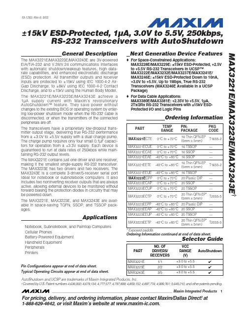
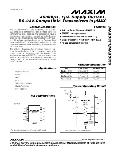
General DescriptionThe MAX3311/MAX3313 are low-power, +5V EIA/TIA-232-compatible transceivers. Both devices have one transmitter and one receiver. The transceivers have a proprietary low-dropout transmitter output stage enabling RS-232-compatible operation from a +5V sup-ply with a single inverting charge pump. These devices require only three 0.1µF capacitors and will run at data rates up to 460kbps while maintaining RS-232-compati-ble output levels.The MAX3311 features a 1µA shutdown mode. In shut-down the device turns off the charge pump, pulls V- to ground, and the transmitter output is disabled. The MAX3313 features an INVALID output that asserts high when an active RS-232 cable signal is connected, sig-naling to the host that a peripheral is connected to the communication port.________________________ApplicationsDigital Cameras PDAs GPS POSTelecommunications Handy Terminals Set-Top BoxesFeatureso 1µA Low-Power Shutdown (MAX3311)o INVALID Output (MAX3313)o Receiver Active in Shutdown (MAX3311)o Single Transceiver (1Tx/1Rx) in 10-Pin µMAX o RS-232-Compatible OperationMAX3311/MAX3313460kbps, 1µA Supply Current,RS-232-Compatible Transceivers in µMAX________________________________________________________________Maxim Integrated Products 1Pin Configurations19-1901; Rev 0; 2/01Ordering InformationFor price, delivery, and to place orders,please contact Maxim Distribution at 1-888-629-4642,or visit Maxim’s website at .Typical Operating CircuitM A X 3311/M A X 3313460kbps, 1µA Supply Current,RS-232-Compatible Transceivers in µMAX 2_________________________________________________________________________________________ABSOLUTE MAXIMUM RATINGSELECTRICAL CHARACTERISTICSStresses beyond those listed under “Absolute Maximum Ratings” may cause permanent damage to the device. These are stress ratings only, and functional operation of the device at these or any other conditions beyond those indicated in the operational sections of the specifications is not implied. Exposure to absolute maximum rating conditions for extended periods may affect device reliability.V CC to GND..............................................................-0.3V to +6V V- to GND.................................................................+0.3V to -7V V CC + |V-|.............................................................................+13V Input VoltagesTIN, SHDN to GND.................................................-0.3V to +6V RIN to GND........................................................................±25V Output VoltagesTOUT to GND..................................................................±13.2V ROUT, INVALID to GND.......................…-0.3V to (V CC + 0.3V)Short-Circuit DurationTOUT to GND...........................................................ContinuousContinuous Power Dissipation10-Pin µMAX (derate 5.6mW/°C above +70°C).............444mW Operating Temperature RangesMAX331_CUB.......................................................0°C to +70°C MAX331_EUB....................................................-40°C to +85°C Junction Temperature......................................................+150°C Storage Temperature Range.............................-65°C to +150°C Lead Temperature (soldering, 10s).................................+300°CMAX3311/MAX3313460kbps, 1µA Supply Current,RS-232-Compatible Transceivers in µMAX_______________________________________________________________________________________3TIMING CHARACTERISTICSELECTRICAL CHARACTERISTICS (continued)M A X 3311/M A X 3313460kbps, 1µA Supply Current,RS-232-Compatible Transceivers in µMAXTypical Operating Characteristics(V CC = +5V, 0.1µF capacitors, transmitter loaded with 3k Ωand C L , T A = +25°C, unless otherwise noted.)0428612101410001500500200025003000SLEW RATEvs. LOAD CAPACITANCELOAD CAPACITANCE (pF)S L E W R A T E (V /µs )-5-4-3-2-10123456050010001500200025003000TRANSMITTER OUTPUT VOLTAGEvs. LOAD CAPACITANCELOAD CAPACITANCE (pF)T R A N S M I T T E R O U T P U T V O L T A G E (V )010001500500200025003000SUPPLY CURRENT vs. LOAD CAPACITANCELOAD CAPACITANCE (pF)MAX3311/MAX3313460kbps, 1µA Supply Current,RS-232-Compatible Transceivers in µMAX_______________________________________________________________________________________5Detailed DescriptionSingle Charge-Pump Voltage ConverterThe MAX3311/MAX3313 internal power supply has a single inverting charge pump that provides a negative voltage from a single +5V supply. The charge pump operates in a discontinuous mode and requires a flying capacitor (C1) and a reservoir capacitor (C2) to gener-ate the V- supply.RS-232-Compatible DriverThe transmitter is an inverting level translator that con-verts CMOS-logic levels to EIA/TIA-232-compatible lev-els. It guarantees data rates up to 460kbps with worst-case loads of 3k Ωin parallel with 1000pF. When SHDN is driven low, the transmitter is disabled and put into three state. The transmitter input does not have an internal pullup resistor.RS-232 ReceiverThe MAX3311/MAX3313 receiver converts RS-232 sig-nals to CMOS-logic output levels. The MAX3311 receiv-er will remain active during shutdown mode. The MAX3313 INVALID indicates when an RS-232 signal is present at the receiver input, and therefore when the port is in use.The MAX3313 INVALID output is pulled low when no valid RS-232 signal level is detected on the receiver input.MAX3311 Shutdown ModeIn shutdown mode, the charge pump is turned off, V- is pulled to ground, and the transmitter output is disabled (Table 1). This reduces supply current typically to 1µA.The time required to exit shutdown is typically less than 100µs.Applications InformationCapacitor SelectionThe capacitor type used for C1 and C2 is not critical for proper operation; either polarized or nonpolarized capacitors are acceptable. If polarized capacitors are used, connect polarity as shown in the Typical Operating Circuit . The charge pump requires 0.1µF capacitors. Increasing the capacitor values (e.g., by afactor of 2) reduces power consumption. C2 can be increased without changing C1’s value. However, do not increase C1’s value without also increasing the value of C2 and C BYPASS to maintain the proper ratios (C1 to the other capacitors).When using the minimum 0.1µF capacitors, make sure the capacitance does not degrade excessively with temperature. If in doubt, use capacitors with a larger nominal value. The capacitor ’s equivalent series resis-tance (ESR) usually rises at low temperatures and influ-ences the amount of ripple on V-.To reduce the output impedance at V-, use larger capacitors (up to 10µF).Bypass V CC to ground with at least 0.1µF. In applica-tions sensitive to power-supply noise generated by the charge pump, decouple V CC to ground with a capaci-tor the same size as (or larger than) charge-pump capacitors C1 and C2.Transmitter Output when ExitingShutdownFigure 1 shows the transmitter output when exiting shutdown mode. The transmitter is loaded with 3k Ωin parallel with 1000pF. The transmitter output displays no ringing or undesirable transients as the MAX3311comes out of shutdown. Note that the transmitter is enabled only when the magnitude of V- exceeds approximately -3V.Figure 1. Transmitter Output when Exiting Shutdown or Powering Up10µs/divTIN = GNDTIN = V CCM A X 3311/M A X 3313High Data RatesThe MAX3311/MAX3313 maintain RS-232-compatible transmitter output voltage (±3.7V minimum) even at high data rates. Figure 2 shows a transmitter loopback test circuit. Figure 3 shows the loopback test result at 120kbps, and Figure 4 shows the same test at 250kbps.460kbps, 1µA Supply Current,RS-232-Compatible Transceivers in µMAX6_______________________________________________________________________Figure 4. Loopback Test Results at 250kbps 2µs/divFigure 3. Loopback Test Results at 120kbps5µs/divFigure 5. Receiver Positive/Negative Thresholds for INVALID-0.3V+2.7V +0.3V0INDETERMINATEINVALID HIGHINVALID LOW460kbps, 1µA Supply Current,RS-232-Compatible Transceivers in µMAXMAX3311/MAX3313Maxim cannot assume responsibility f or use of any circuitry other than circuitry entirely embodied in a Maxim product. No circuit patent licenses are implied. Maxim reserves the right to change the circuitry and specifications without notice at any time.Maxim Integrated Products, 120 San Gabriel Drive, Sunnyvale, CA 94086 408-737-7600 _____________________7©2001 Maxim Integrated ProductsPrinted USAis a registered trademark of Maxim Integrated Products.Package InformationChip InformationTRANSISTOR COUNT: 278Pin Configurations (continued)。
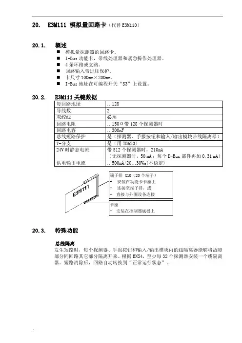
20. E3M111 模拟量回路卡(代替E3M110)20.1.概述⏹模拟量探测器的回路卡。
⏹I-Bus功能卡,带线处理器和紧急操作处理器。
⏹4条环路或支路。
⏹回路输入带过压保护。
⏹卡尺寸100mm×200mm。
⏹I-Bus地址在可编程开关“S3”上设置。
20.2.E3M111关键数据每回路地址 (128)导线数 2双绞线必须回路电阻…150Ω带128个探测器时回路电容…300nF总线短路保护是(探测器、手报按钮和输入/输出模块带线隔离器)T-分支是(用TB620)24V时静态电流带512个探测器时,210mA(无探测器时,50 mA ;每个D-Bus部件再加0.31 mA)供电输出电流…500mA/20…30V DC(不稳定)端子排 X10(20个端子)-安装在功能卡卡座上-连接至端子排,或- 直接与外围设备连接卡座- 安装在控制器底板上20.3.特殊功能总线隔离发生短路时,每个探测器、手报按钮和输入/输出模块内的线隔离器能够将故障部分同回路其它部分隔离开来。
根据EN54,至少每32个探测器安装一个线隔离器。
短路消除后,回路自动转换到“正常运行状态”。
20.4.重要部件❶保险丝F1...F16, F19/20 1A/T**回路1 (4)** SMD保险丝(只可在厂家更换)❷保险丝F17 1A/F**功能卡供电24V❸保险丝F18 1A/F**功能卡供电5V*高熔断特性保险丝❹扁平电缆插头“ST1”(26-针):I-Bus❺插接端子“K1”:对“I-Bus”功能卡供电❻可编程开关“S3”:“I-Bus地址”设置❼调试LED “H1”:闪亮 =和探测回路接通持续 =部件可能故障灭 =未连接回路,或未编程❽插口“ST10”:应急显示(只在“应急火警”时启动)❾保险丝F19/20 1A/T** DC-模块供电电压** SMD保险丝(只可在厂家更换)20.5.可编程开关“S3”用于设置I-Bus地址。
电压-频率变换器LM331LM331是美国NS公司生产的性能价格比较高的集成芯片。
LM331可用作精密的频率电压(F/V)转换器、A/D转换器、线性频率调制解调、长时间积分器以及其他相关的器件。
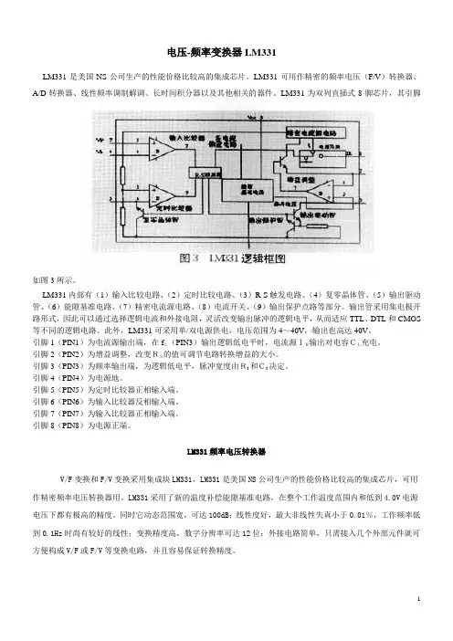
LM331为双列直插式8脚芯片,其引脚如图3所示。
LM331内部有(1)输入比较电路、(2)定时比较电路、(3)R-S触发电路、(4)复零晶体管、(5)输出驱动管、(6)能隙基准电路、(7)精密电流源电路、(8)电流开关、(9)输出保护点路等部分。
输出管采用集电极开路形式,因此可以通过选择逻辑电流和外接电阻,灵活改变输出脉冲的逻辑电平,从而适应TTL、DTL和CMOS 等不同的逻辑电路。
此外,LM331可采用单/双电源供电,电压范围为4~40V,输出也高达40V。
引脚1(PIN1)为电流源输出端,在f0(PIN3)输出逻辑低电平时,电流源IR输出对电容CL充电。
引脚2(PIN2)为增益调整,改变RS的值可调节电路转换增益的大小。
引脚3(PIN3)为频率输出端,为逻辑低电平,脉冲宽度由Rt和Ct决定。
引脚4(PIN4)为电源地。
引脚5(PIN5)为定时比较器正相输入端。
引脚6(PIN6)为输入比较器反相输入端。
引脚7(PIN7)为输入比较器正相输入端。
引脚8(PIN8)为电源正端。
LM331频率电压转换器V/F变换和F/V变换采用集成块LM331,LM331是美国NS公司生产的性能价格比较高的集成芯片,可用作精密频率电压转换器用。
LM331采用了新的温度补偿能隙基准电路,在整个工作温度范围内和低到4.0V电源电压下都有极高的精度。
同时它动态范围宽,可达100dB;线性度好,最大非线性失真小于0.01%,工作频率低到0.1Hz时尚有较好的线性;变换精度高,数字分辨率可达12位;外接电路简单,只需接入几个外部元件就可方便构成V/F或F/V等变换电路,并且容易保证转换精度。
图2是由LM331组成的电压频率变换电路,LM331内部由输入比较器、定时比较器、R-S触发器、输出驱动、复零晶体管、能隙基准电路和电流开关等部分组成。
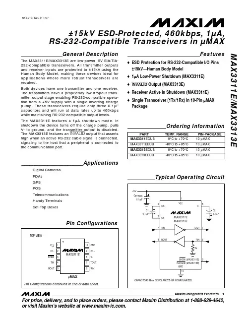
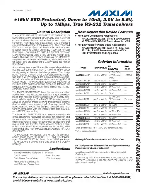
General DescriptionThe MAX3311E/MAX3313E are low-power, 5V EIA/TIA-232-compatible transceivers. All transmitter outputs and receiver inputs are protected to ±15kV using the Human Body Model, making these devices ideal for applications where more robust transceivers are required.Both devices have one transmitter and one receiver.The transmitters have a proprietary low-dropout trans-mitter output stage enabling RS-232-compatible opera-tion from a +5V supply with a single inverting charge pump. These transceivers require only three 0.1µF capacitors and will run at data rates up to 460kbps while maintaining RS-232-compatible output levels.The MAX3311E features a 1µA shutdown mode. In shutdown the device turns off the charge pump, pulls V- to ground, and the transmitter output is disabled.The MAX3313E features an INVALID output that asserts high when an active RS-232 cable signal is connected,signaling to the host that a peripheral is connected to the communication port.________________________ApplicationsDigital Cameras PDAs GPS POSTelecommunications Handy Terminals Set-Top BoxesFeatureso ESD Protection for RS-232-Compatible I/O Pins±15kV—Human Body Modelo 1µA Low-Power Shutdown (MAX3311E)o INVALID Output (MAX3313E)o Receiver Active in Shutdown (MAX3311E)o Single Transceiver (1Tx/1Rx) in 10-Pin µMAX PackageMAX3311E/MAX3313E±15kV ESD-Protected, 460kbps, 1µA,RS-232-Compatible Transceivers in µMAX________________________________________________________________Maxim Integrated Products1Pin Configurations19-1910; Rev 0; 1/01Ordering InformationFor price, delivery, and to place orders,please contact Maxim Distribution at 1-888-629-4642,or visit Maxim’s website at .Typical Operating CircuitM A X 3311E /M A X 3313E±15kV ESD-Protected, 460kbps, 1µA,RS-232-Compatible Transceivers in µMAX 2_______________________________________________________________________________________ABSOLUTE MAXIMUM RATINGSELECTRICAL CHARACTERISTICSStresses beyond those listed under “Absolute Maximum Ratings” may cause permanent damage to the device. These are stress ratings only, and functional operation of the device at these or any other conditions beyond those indicated in the operational sections of the specifications is not implied. Exposure to absolute maximum rating conditions for extended periods may affect device reliability.V CC to GND.............................................................-0.3V to +6V V- to GND................................................................+0.3V to -7V V CC + |V-|............................................................................+13V Input VoltagesTIN, SHDN to GND...............................................-0.3V to +6V RIN to GND......................................................................±25V Output VoltagesTOUT to GND................................................................±13.2V ROUT, INVALID to GND.....................…-0.3V to (V CC + 0.3V)Short-Circuit DurationTOUT to GND.........................................................ContinuousContinuous Power Dissipation10-Pin µMAX (derate 5.6mW/°C above +70°C)..........444mW Operating Temperature RangesMAX331_ECUB.................................................0°C to +70°C MAX331_EEUB..............................................-40°C to +85°C Junction Temperature.....................................................+150°C Storage Temperature Range............................-65°C to +150°C Lead Temperature (soldering, 10s)................................+300°CMAX3311E/MAX3313E±15kV ESD-Protected, 460kbps, 1µA,RS-232-Compatible Transceivers in µMAX_______________________________________________________________________________________3ELECTRICAL CHARACTERISTICS (continued)TIMING CHARACTERISTICSM A X 3311E /M A X 3313E±15kV ESD-Protected, 460kbps, 1µA,RS-232-Compatible Transceivers in µMAX 4_______________________________________________________________________________________Typical Operating Characteristics(V CC = +5V, 0.1µF capacitors, transmitter loaded with 3k Ωand C L , T A = +25°C, unless otherwise noted.)0428612101410001500500200025003000SLEW RATEvs. LOAD CAPACITANCELOAD CAPACITANCE (pF)S L E W R A T E (V /µs )-5-4-3-2-10123456050010001500200025003000TRANSMITTER OUTPUT VOLTAGEvs. LOAD CAPACITANCELOAD CAPACITANCE (pF)T R A N S M I T T E R O U T P U T V O L T A G E (V )010001500500200025003000SUPPLY CURRENT vs. LOAD CAPACITANCELOAD CAPACITANCE (pF)Detailed DescriptionSingle Charge-Pump Voltage ConverterThe MAX3311E/MAX3313E internal power supply has a single inverting charge pump that provides a negative voltage from a single +5V supply. The charge pump operates in a discontinuous mode and requires a flying capacitor (C1) and a reservoir capacitor (C2) to gener-ate the V- supply.RS-232-Compatible DriverThe transmitter is an inverting level translator that con-verts CMOS-logic levels to EIA/TIA-232 compatible lev-els. It guarantees data rates up to 460kbps with worst-case loads of 3k Ωin parallel with 1000pF. When SHDN is driven low, the transmitter is disabled and put into tri-state. The transmitter input does not have an internal pullup resistor.RS-232 ReceiverThe MAX3311E/MAX3313E receiver converts RS-232signals to CMOS-logic output levels. The MAX3311E receiver will remain active during shutdown mode. The MAX3313E INVALID indicates when an RS-232 signal is present at the receiver input, and therefore when the port is in use.The MAX3313E INVALID output is pulled low when no valid RS-232 signal level is detected on the receiver input.MAX3311E Shutdown ModeIn shutdown mode, the charge pump is turned off, V- is pulled to ground, and the transmitter output is disabled (Table 1). This reduces supply current typically to 1µA.The time required to exit shutdown is less than 25ms.Applications InformationCapacitor SelectionThe capacitor type used for C1 and C2 is not critical for proper operation; either polarized or nonpolarized capacitors are acceptable. If polarized capacitors are used, connect polarity as shown in the Typical Operating Circuit . The charge pump requires 0.1µF capacitors. Increasing the capacitor values (e.g., by a factor of 2) reduces power consumption. C2 can beincreased without changing C1’s value. However, do not increase C1’s value without also increasing the value of C2 and C BYPASS to maintain the proper ratios (C1 to the other capacitors).When using the minimum 0.1µF capacitors, make sure the capacitance does not degrade excessively with temperature. If in doubt, use capacitors with a larger nominal value. The capacitor ’s equivalent series resis-tance (ESR) usually rises at low temperatures and influ-ences the amount of ripple on V-.To reduce the output impedance at V-, use larger capacitors (up to 10µF).Bypass V CC to ground with at least 0.1µF. In applica-tions sensitive to power-supply noise generated by the charge pump, decouple V CC to ground with a capaci-tor the same size as (or larger than) charge-pump capacitors C1 and C2.Transmitter Output when ExitingShutdownFigure 1 shows the transmitter output when exiting shutdown mode. The transmitter is loaded with 3k Ωin parallel with 1000pF. The transmitter output displays no ringing or undesirable transients as the MAX3311E comes out of shutdown. Note that the transmitter is enabled only when the magnitude of V- exceeds approximately -3V.High Data RatesThe MAX3311E/MAX3313E maintain RS-232-compati-ble ±3.7V minimum transmitter output voltage even atMAX3311E/MAX3313E±15kV ESD-Protected, 460kbps, 1µA,RS-232-Compatible Transceivers in µMAX5Figure 1. Transmitter Output when Exiting Shutdown or Powering Up10µs/divSHDNTOUT5V/div1.5V/divTIN = GNDTIN = V CCM A X 3311E /M A X 3313E±15kV ESD-Protected, 460kbps, 1µA,RS-232-Compatible Transceivers in µMAX 6_______________________________________________________________________________________high data rates. Figure 2 shows a transmitter loopback test circuit. Figure 3 shows the loopback test result at 120kbps, and Figure 4 shows the same test at 250kbps.±15kV ESD ProtectionAs with all Maxim devices, ESD-protection structures are incorporated on all pins to protect against electro-static discharges encountered during handling and assembly. The MAX3311E/MAX3313E driver outputsand receiver inputs have extra protection against static discharge. Maxim ’s engineers have developed state-of-the-art structures to protect these pins against ESD of ±15kV without damage. The ESD structures withstand high ESD in all states: normal operation, shutdown, and powered down. After an ESD event, Maxim ’s E versions keep working without latchup; whereas, competing products can latch and must be powered down to remove latchup.ESD protection can be tested in various ways. The transmitter outputs and receiver inputs of the product family are characterized for protection to ±15kV using the Human Body Model.ESD Test ConditionsESD performance depends on a variety of conditions.Contact Maxim for a reliability report that documents test setup, test methodology, and test results.Human Body ModelFigure 5 shows the Human Body Model, and Figure 6shows the current waveform it generates when dis-charged into low impedance. This model consists of a 100pF capacitor charged to the ESD voltage of interest,which is then discharged into the test device through a 1.5k Ωresistor.Machine ModelThe Machine Model for ESD tests all pins using a 200pF storage capacitor and zero discharge resis-tance. Its objective is to emulate the stress caused by contact that occurs with handling and assembly during manufacturing. Of course, all pins require this protec-tion during manufacturing, not just RS-232 inputs and outputs. Therefore, after PC board assembly, the Machine Model is less relevant to I/O ports.Figure 4. Loopback Test Results at 250kbps2µs/divTOUTTINROUTFigure 3. Loopback Test Results at 120kbps 5µs/divTOUTTINROUTMAX3311E/MAX3313E±15kV ESD-Protected, 460kbps, 1µA,RS-232-Compatible Transceivers in µMAX_______________________________________________________________________________________7Figure 5. Human Body ESD Test ModelFigure 6. Human Body Current WaveformPin Configurations (continued)Chip InformationTRANSISTOR COUNT: 278M A X 3311E /M A X 3313E±15kV ESD-Protected, 460kbps, 1µA,RS-232-Compatible Transceivers in µMAX Maxim cannot assume responsibility for use of any circuitry other than circuitry entirely embodied in a Maxim product. No circuit patent licenses are implied. Maxim reserves the right to change the circuitry and specifications without notice at any time.8_____________________Maxim Integrated Products, 120 San Gabriel Drive, Sunnyvale, CA 94086 408-737-7600©2001 Maxim Integrated ProductsPrinted USAis a registered trademark of Maxim Integrated Products.______________________________________________________________Pin Description。
PACKAGING INFORMATIONOrderable Device Status(1)PackageType PackageDrawingPins PackageQtyEco Plan(2)Lead/Ball Finish MSL Peak Temp(3)MAX3221CDB ACTIVE SSOP DB1680Green(RoHS&no Sb/Br)CU NIPDAU Level-1-260C-UNLIMMAX3221CDBE4ACTIVE SSOP DB1680Green(RoHS&no Sb/Br)CU NIPDAU Level-1-260C-UNLIMMAX3221CDBG4ACTIVE SSOP DB1680Green(RoHS&no Sb/Br)CU NIPDAU Level-1-260C-UNLIMMAX3221CDBR ACTIVE SSOP DB162000Green(RoHS&no Sb/Br)CU NIPDAU Level-1-260C-UNLIMMAX3221CDBRG4ACTIVE SSOP DB162000Green(RoHS&no Sb/Br)CU NIPDAU Level-1-260C-UNLIMMAX3221CPW ACTIVE TSSOP PW1690Green(RoHS&no Sb/Br)CU NIPDAU Level-1-260C-UNLIMMAX3221CPWE4ACTIVE TSSOP PW1690Green(RoHS&no Sb/Br)CU NIPDAU Level-1-260C-UNLIMMAX3221CPWG4ACTIVE TSSOP PW1690Green(RoHS&no Sb/Br)CU NIPDAU Level-1-260C-UNLIMMAX3221CPWR ACTIVE TSSOP PW162000Green(RoHS&no Sb/Br)CU NIPDAU Level-1-260C-UNLIMMAX3221CPWRE4ACTIVE TSSOP PW162000Green(RoHS&no Sb/Br)CU NIPDAU Level-1-260C-UNLIMMAX3221CPWRG4ACTIVE TSSOP PW162000Green(RoHS&no Sb/Br)CU NIPDAU Level-1-260C-UNLIMMAX3221IDB ACTIVE SSOP DB1680Green(RoHS&no Sb/Br)CU NIPDAU Level-1-260C-UNLIMMAX3221IDBE4ACTIVE SSOP DB1680Green(RoHS&no Sb/Br)CU NIPDAU Level-1-260C-UNLIMMAX3221IDBG4ACTIVE SSOP DB1680Green(RoHS&no Sb/Br)CU NIPDAU Level-1-260C-UNLIMMAX3221IDBR ACTIVE SSOP DB162000Green(RoHS&no Sb/Br)CU NIPDAU Level-1-260C-UNLIMMAX3221IDBRE4ACTIVE SSOP DB162000Green(RoHS&no Sb/Br)CU NIPDAU Level-1-260C-UNLIMMAX3221IDBRG4ACTIVE SSOP DB162000Green(RoHS&no Sb/Br)CU NIPDAU Level-1-260C-UNLIMMAX3221IPW ACTIVE TSSOP PW1690Green(RoHS&no Sb/Br)CU NIPDAU Level-1-260C-UNLIMMAX3221IPWE4ACTIVE TSSOP PW1690Green(RoHS&no Sb/Br)CU NIPDAU Level-1-260C-UNLIMMAX3221IPWG4ACTIVE TSSOP PW1690Green(RoHS&no Sb/Br)CU NIPDAU Level-1-260C-UNLIMMAX3221IPWR ACTIVE TSSOP PW162000Green(RoHS&no Sb/Br)CU NIPDAU Level-1-260C-UNLIMMAX3221IPWRE4ACTIVE TSSOP PW162000Green(RoHS&no Sb/Br)CU NIPDAU Level-1-260C-UNLIMMAX3221IPWRG4ACTIVE TSSOP PW162000Green(RoHS&no Sb/Br)CU NIPDAU Level-1-260C-UNLIM(1)The marketing status values are defined as follows:ACTIVE:Product device recommended for new designs.LIFEBUY:TI has announced that the device will be discontinued,and a lifetime-buy period is in effect.NRND:Not recommended for new designs.Device is in production to support existing customers,but TI does not recommend using this part in a new design.PREVIEW:Device has been announced but is not in production.Samples may or may not be available.OBSOLETE:TI has discontinued the production of the device.(2)Eco Plan-The planned eco-friendly classification:Pb-Free(RoHS),Pb-Free(RoHS Exempt),or Green(RoHS&no Sb/Br)-please check /productcontent for the latest availability information and additional product content details.TBD:The Pb-Free/Green conversion plan has not been defined.Pb-Free(RoHS):TI's terms"Lead-Free"or"Pb-Free"mean semiconductor products that are compatible with the current RoHS requirements for all6substances,including the requirement that lead not exceed0.1%by weight in homogeneous materials.Where designed to be soldered at high temperatures,TI Pb-Free products are suitable for use in specified lead-free processes.Pb-Free(RoHS Exempt):This component has a RoHS exemption for either1)lead-based flip-chip solder bumps used between the die and package,or2)lead-based die adhesive used between the die and leadframe.The component is otherwise considered Pb-Free(RoHS compatible)as defined above.Green(RoHS&no Sb/Br):TI defines"Green"to mean Pb-Free(RoHS compatible),and free of Bromine(Br)and Antimony(Sb)based flame retardants(Br or Sb do not exceed0.1%by weight in homogeneous material)(3)MSL,Peak Temp.--The Moisture Sensitivity Level rating according to the JEDEC industry standard classifications,and peak solder temperature.Important Information and Disclaimer:The information provided on this page represents TI's knowledge and belief as of the date that it is provided.TI bases its knowledge and belief on information provided by third parties,and makes no representation or warranty as to the accuracy of such information.Efforts are underway to better integrate information from third parties.TI has taken and continues to take reasonable steps to provide representative and accurate information but may not have conducted destructive testing or chemical analysis on incoming materials and chemicals.TI and TI suppliers consider certain information to be proprietary,and thus CAS numbers and other limited information may not be available for release.In no event shall TI's liability arising out of such information exceed the total purchase price of the TI part(s)at issue in this document sold by TI to Customer on an annual basis.OTHER QUALIFIED VERSIONS OF MAX3221:•Enhanced Product:MAX3221-EPNOTE:Qualified Version Definitions:•Enhanced Product-Supports Defense,Aerospace and Medical ApplicationsTAPE AND REEL INFORMATION*All dimensions are nominalDevicePackage Type Package Drawing Pins SPQReel Diameter (mm)Reel Width W1(mm)A0(mm)B0(mm)K0(mm)P1(mm)W (mm)Pin1Quadrant MAX3221CDBR SSOP DB 162000330.016.48.2 6.6 2.512.016.0Q1MAX3221CPWR TSSOP PW 162000330.012.47.0 5.6 1.68.012.0Q1MAX3221IDBR SSOP DB 162000330.016.48.2 6.6 2.512.016.0Q1MAX3221IPWRTSSOPPW162000330.012.47.05.61.68.012.0Q1*All dimensions are nominalDevice Package Type Package Drawing Pins SPQ Length(mm)Width(mm)Height(mm) MAX3221CDBR SSOP DB162000346.0346.033.0 MAX3221CPWR TSSOP PW162000346.0346.029.0 MAX3221IDBR SSOP DB162000346.0346.033.0 MAX3221IPWR TSSOP PW162000346.0346.029.0IMPORTANT NOTICETexas Instruments Incorporated and its subsidiaries(TI)reserve the right to make corrections,modifications,enhancements,improvements, and other changes to its products and services at any time and to discontinue any product or service without notice.Customers should obtain the latest relevant information before placing orders and should verify that such information is current and complete.All products are sold subject to TI’s terms and conditions of sale supplied at the time of order acknowledgment.TI warrants performance of its hardware products to the specifications applicable at the time of sale in accordance with TI’s standard warranty.Testing and other quality control techniques are used to the extent TI deems necessary to support this warranty.Except where mandated by government requirements,testing of all parameters of each product is not necessarily performed.TI assumes no liability for applications assistance or customer product design.Customers are responsible for their products and applications using TI components.To minimize the risks associated with customer products and applications,customers should provide adequate design and operating safeguards.TI does not warrant or represent that any license,either express or implied,is granted under any TI patent right,copyright,mask work right, or other TI intellectual property right relating to any combination,machine,or process in which TI products or services are rmation published by TI regarding third-party products or services does not constitute a license from TI to use such products or services or a warranty or endorsement e of such information may require a license from a third party under the patents or other intellectual property of the third party,or a license from TI under the patents or other intellectual property of TI.Reproduction of TI information in TI data books or data sheets is permissible only if reproduction is without alteration and is accompanied by all associated warranties,conditions,limitations,and notices.Reproduction of this information with alteration is an unfair and deceptive business practice.TI is not responsible or liable for such altered rmation of third parties may be subject to additional restrictions.Resale of TI products or services with statements different from or beyond the parameters stated by TI for that product or service voids all express and any implied warranties for the associated TI product or service and is an unfair and deceptive business practice.TI is not responsible or liable for any such statements.TI products are not authorized for use in safety-critical applications(such as life support)where a failure of the TI product would reasonably be expected to cause severe personal injury or death,unless officers of the parties have executed an agreement specifically governing such use.Buyers represent that they have all necessary expertise in the safety and regulatory ramifications of their applications,and acknowledge and agree that they are solely responsible for all legal,regulatory and safety-related requirements concerning their products and any use of TI products in such safety-critical applications,notwithstanding any applications-related information or support that may be provided by TI.Further,Buyers must fully indemnify TI and its representatives against any damages arising out of the use of TI products in such safety-critical applications.TI products are neither designed nor intended for use in military/aerospace applications or environments unless the TI products are specifically designated by TI as military-grade or"enhanced plastic."Only products designated by TI as military-grade meet military specifications.Buyers acknowledge and agree that any such use of TI products which TI has not designated as military-grade is solely at the Buyer's risk,and that they are solely responsible for compliance with all legal and regulatory requirements in connection with such use. TI products are neither designed nor intended for use in automotive applications or environments unless the specific TI products are designated by TI as compliant with ISO/TS16949requirements.Buyers acknowledge and agree that,if they use any non-designated products in automotive applications,TI will not be responsible for any failure to meet such requirements.Following are URLs where you can obtain information on other Texas Instruments products and application solutions:Products ApplicationsAmplifiersAudioData Converters AutomotiveDSP BroadbandClocks and Timers Digital ControlInterface MedicalLogic MilitaryPower Mgmt Optical NetworkingMicrocontrollers SecurityRFID TelephonyRF/IF and ZigBee®Solutions Video&ImagingWirelessMailing Address:Texas Instruments,Post Office Box655303,Dallas,Texas75265Copyright©2008,Texas Instruments Incorporated元器件交易网。
Maxim产品命名规则MAXIM前缀是“MAX”。
DALLAS则是以“DS”开头。
MAX×××或MAX××××说明:1后缀CSA、CWA 其中C表示普通级,S表示表贴,W表示宽体表贴。
2 后缀CWI表示宽体表贴,EEWI宽体工业级表贴,后缀MJA或883为军级。
3 CPA、BCPI、BCPP、CPP、CCPP、CPE、CPD、ACPA后缀均为普通双列直插。
举例MAX202CPE、CPE普通ECPE普通带抗静电保护MAX202EEPE 工业级抗静电保护(-45℃-85℃)说明 E指抗静电保护MAXIM数字排列分类1字头模拟器 2字头滤波器 3字头多路开关4字头放大器 5字头数模转换器 6字头电压基准7字头电压转换 8字头复位器 9字头比较器自主产品的命名规则绝大多数Maxim产品采用公司专有的命名系统,包括基础型号和后续的3个或4个字母尾缀,有时还带有其它标识符号。
例如:{MAX9722} {AETE} {+T}( A ) ( B) ( C)--------------------------------------------------------------------------------(A)是基础型号基本型号(也称为基础型号)用于区分不同的产品类型,与封装、温度及其它参量无关。
精度等级等参量通常用型号尾缀表示,有些情况下会为不同参量的器件分配一个新的基本型号。
--------------------------------------------------------------------------------(B)是3字母或4字母尾缀器件具有4个尾缀字母时,第一个尾标代表产品的等级(精度、电压规格、速率等)。
例如:MAX631ACPA中,第一个尾标"A"表示5%的输出精度。
产品数据资料中给出了型号对应的等级。
贴片电容标331 -回复“贴片电容标331”的全称是“贴片多层陶瓷电容标准型号331”,是一种常见的电子元件。
本文将围绕贴片电容标331展开详细介绍,包括其定义、结构、特点、应用领域、选择与购买、使用注意事项等内容。
第一节:定义(150字)贴片电容标331是一种多层陶瓷贴片电容器,属于标准型号,其型号编码为331。
具有固定的电容值和尺寸,适用于广泛的电子电路应用。
第二节:结构(150字)贴片电容标331的结构包括多层陶瓷片和金属电极。
多层陶瓷片由陶瓷材料制成,上面涂覆有导电材料形成电极。
多个陶瓷片相互叠加,形成具有特定电容值的电容器。
两端的金属电极用于引出电容器的正负极。
第三节:特点(200字)贴片电容标331具有以下几个特点:1. 尺寸小巧:由于采用贴片结构,贴片电容标331的尺寸非常小,适合密集的电路板布局。
2. 电容值稳定:多层陶瓷片的结构使得贴片电容标331的电容值稳定,不易受温度和频率的影响。
3. 工作频率宽:贴片电容标331的工作频率范围广,适用于高频和低频电路。
4. 低ESR:贴片电容标331的等效串联电阻(ESR)较低,能够提供良好的电容性能。
5. 高温度耐受性:贴片电容标331能够在较高的温度下正常工作,适用于一些特殊环境。
第四节:应用领域(250字)贴片电容标331广泛应用于各种电子设备和电路中,包括但不限于以下领域:1. 智能手机和平板电脑:在小尺寸的手机和平板电脑中,贴片电容标331被用于电源管理、信号传输和滤波等电路中。
2. 通信设备:在通讯设备中,贴片电容标331可以用于天线匹配电路、滤波电路和耦合电路等。
3. 计算机:在计算机主板和外部设备中,贴片电容标331可应用于电源滤波、去耦等关键电路中。
4. 汽车电子:在汽车电子控制系统中,贴片电容标331可用于发动机控制单元、电动助力转向系统等。
5. 工业控制:贴片电容标331也应用于工业控制设备中,如PLC(可编程逻辑控制器)、变频器等。
General DescriptionThe MAX3311E/MAX3313E are low-power, 5V EIA/TIA-232-compatible transceivers. All transmitter outputs and receiver inputs are protected to ±15kV using the Human Body Model, making these devices ideal for applications where more robust transceivers are required.Both devices have one transmitter and one receiver.The transmitters have a proprietary low-dropout trans-mitter output stage enabling RS-232-compatible opera-tion from a +5V supply with a single inverting charge pump. These transceivers require only three 0.1µF capacitors and will run at data rates up to 460kbps while maintaining RS-232-compatible output levels.The MAX3311E features a 1µA shutdown mode. In shutdown the device turns off the charge pump, pulls V- to ground, and the transmitter output is disabled.The MAX3313E features an INVALID output that asserts high when an active RS-232 cable signal is connected,signaling to the host that a peripheral is connected to the communication port.________________________ApplicationsDigital Cameras PDAs GPS POSTelecommunications Handy Terminals Set-Top BoxesFeatureso ESD Protection for RS-232-Compatible I/O Pins±15kV—Human Body Modelo 1µA Low-Power Shutdown (MAX3311E)o INVALID Output (MAX3313E)o Receiver Active in Shutdown (MAX3311E)o Single Transceiver (1Tx/1Rx) in 10-Pin µMAX PackageMAX3311E/MAX3313E±15kV ESD-Protected, 460kbps, 1µA,RS-232-Compatible Transceivers in µMAX________________________________________________________________Maxim Integrated Products1Pin Configurations19-1910; Rev 0; 1/01Ordering InformationFor price, delivery, and to place orders,please contact Maxim Distribution at 1-888-629-4642,or visit Maxim’s website at .Typical Operating CircuitM A X 3311E /M A X 3313E±15kV ESD-Protected, 460kbps, 1µA,RS-232-Compatible Transceivers in µMAX 2_______________________________________________________________________________________ABSOLUTE MAXIMUM RATINGSELECTRICAL CHARACTERISTICSStresses beyond those listed under “Absolute Maximum Ratings” may cause permanent damage to the device. These are stress ratings only, and functional operation of the device at these or any other conditions beyond those indicated in the operational sections of the specifications is not implied. Exposure to absolute maximum rating conditions for extended periods may affect device reliability.V CC to GND.............................................................-0.3V to +6V V- to GND................................................................+0.3V to -7V V CC + |V-|............................................................................+13V Input VoltagesTIN, SHDN to GND...............................................-0.3V to +6V RIN to GND......................................................................±25V Output VoltagesTOUT to GND................................................................±13.2V ROUT, INVALID to GND.....................…-0.3V to (V CC + 0.3V)Short-Circuit DurationTOUT to GND.........................................................ContinuousContinuous Power Dissipation10-Pin µMAX (derate 5.6mW/°C above +70°C)..........444mW Operating Temperature RangesMAX331_ECUB.................................................0°C to +70°C MAX331_EEUB..............................................-40°C to +85°C Junction Temperature.....................................................+150°C Storage Temperature Range............................-65°C to +150°C Lead Temperature (soldering, 10s)................................+300°CMAX3311E/MAX3313E±15kV ESD-Protected, 460kbps, 1µA,RS-232-Compatible Transceivers in µMAX_______________________________________________________________________________________3ELECTRICAL CHARACTERISTICS (continued)TIMING CHARACTERISTICSM A X 3311E /M A X 3313E±15kV ESD-Protected, 460kbps, 1µA,RS-232-Compatible Transceivers in µMAX 4_______________________________________________________________________________________Typical Operating Characteristics(V CC = +5V, 0.1µF capacitors, transmitter loaded with 3k Ωand C L , T A = +25°C, unless otherwise noted.)0428612101410001500500200025003000SLEW RATEvs. LOAD CAPACITANCELOAD CAPACITANCE (pF)S L E W R A T E (V /µs )-5-4-3-2-10123456050010001500200025003000TRANSMITTER OUTPUT VOLTAGEvs. LOAD CAPACITANCELOAD CAPACITANCE (pF)T R A N S M I T T E R O U T P U T V O L T A G E (V )010001500500200025003000SUPPLY CURRENT vs. LOAD CAPACITANCELOAD CAPACITANCE (pF)Detailed DescriptionSingle Charge-Pump Voltage ConverterThe MAX3311E/MAX3313E internal power supply has a single inverting charge pump that provides a negative voltage from a single +5V supply. The charge pump operates in a discontinuous mode and requires a flying capacitor (C1) and a reservoir capacitor (C2) to gener-ate the V- supply.RS-232-Compatible DriverThe transmitter is an inverting level translator that con-verts CMOS-logic levels to EIA/TIA-232 compatible lev-els. It guarantees data rates up to 460kbps with worst-case loads of 3k Ωin parallel with 1000pF. When SHDN is driven low, the transmitter is disabled and put into tri-state. The transmitter input does not have an internal pullup resistor.RS-232 ReceiverThe MAX3311E/MAX3313E receiver converts RS-232signals to CMOS-logic output levels. The MAX3311E receiver will remain active during shutdown mode. The MAX3313E INVALID indicates when an RS-232 signal is present at the receiver input, and therefore when the port is in use.The MAX3313E INVALID output is pulled low when no valid RS-232 signal level is detected on the receiver input.MAX3311E Shutdown ModeIn shutdown mode, the charge pump is turned off, V- is pulled to ground, and the transmitter output is disabled (Table 1). This reduces supply current typically to 1µA.The time required to exit shutdown is less than 25ms.Applications InformationCapacitor SelectionThe capacitor type used for C1 and C2 is not critical for proper operation; either polarized or nonpolarized capacitors are acceptable. If polarized capacitors are used, connect polarity as shown in the Typical Operating Circuit . The charge pump requires 0.1µF capacitors. Increasing the capacitor values (e.g., by a factor of 2) reduces power consumption. C2 can beincreased without changing C1’s value. However, do not increase C1’s value without also increasing the value of C2 and C BYPASS to maintain the proper ratios (C1 to the other capacitors).When using the minimum 0.1µF capacitors, make sure the capacitance does not degrade excessively with temperature. If in doubt, use capacitors with a larger nominal value. The capacitor ’s equivalent series resis-tance (ESR) usually rises at low temperatures and influ-ences the amount of ripple on V-.To reduce the output impedance at V-, use larger capacitors (up to 10µF).Bypass V CC to ground with at least 0.1µF. In applica-tions sensitive to power-supply noise generated by the charge pump, decouple V CC to ground with a capaci-tor the same size as (or larger than) charge-pump capacitors C1 and C2.Transmitter Output when ExitingShutdownFigure 1 shows the transmitter output when exiting shutdown mode. The transmitter is loaded with 3k Ωin parallel with 1000pF. The transmitter output displays no ringing or undesirable transients as the MAX3311E comes out of shutdown. Note that the transmitter is enabled only when the magnitude of V- exceeds approximately -3V.High Data RatesThe MAX3311E/MAX3313E maintain RS-232-compati-ble ±3.7V minimum transmitter output voltage even atMAX3311E/MAX3313E±15kV ESD-Protected, 460kbps, 1µA,RS-232-Compatible Transceivers in µMAX5Figure 1. Transmitter Output when Exiting Shutdown or Powering Up10µs/divSHDNTOUT5V/div1.5V/divTIN = GNDTIN = V CCM A X 3311E /M A X 3313E±15kV ESD-Protected, 460kbps, 1µA,RS-232-Compatible Transceivers in µMAX 6_______________________________________________________________________________________high data rates. Figure 2 shows a transmitter loopback test circuit. Figure 3 shows the loopback test result at 120kbps, and Figure 4 shows the same test at 250kbps.±15kV ESD ProtectionAs with all Maxim devices, ESD-protection structures are incorporated on all pins to protect against electro-static discharges encountered during handling and assembly. The MAX3311E/MAX3313E driver outputsand receiver inputs have extra protection against static discharge. Maxim ’s engineers have developed state-of-the-art structures to protect these pins against ESD of ±15kV without damage. The ESD structures withstand high ESD in all states: normal operation, shutdown, and powered down. After an ESD event, Maxim ’s E versions keep working without latchup; whereas, competing products can latch and must be powered down to remove latchup.ESD protection can be tested in various ways. The transmitter outputs and receiver inputs of the product family are characterized for protection to ±15kV using the Human Body Model.ESD Test ConditionsESD performance depends on a variety of conditions.Contact Maxim for a reliability report that documents test setup, test methodology, and test results.Human Body ModelFigure 5 shows the Human Body Model, and Figure 6shows the current waveform it generates when dis-charged into low impedance. This model consists of a 100pF capacitor charged to the ESD voltage of interest,which is then discharged into the test device through a 1.5k Ωresistor.Machine ModelThe Machine Model for ESD tests all pins using a 200pF storage capacitor and zero discharge resis-tance. Its objective is to emulate the stress caused by contact that occurs with handling and assembly during manufacturing. Of course, all pins require this protec-tion during manufacturing, not just RS-232 inputs and outputs. Therefore, after PC board assembly, the Machine Model is less relevant to I/O ports.Figure 4. Loopback Test Results at 250kbps2µs/divTOUTTINROUTFigure 3. Loopback Test Results at 120kbps 5µs/divTOUTTINROUTMAX3311E/MAX3313E±15kV ESD-Protected, 460kbps, 1µA,RS-232-Compatible Transceivers in µMAX_______________________________________________________________________________________7Figure 5. Human Body ESD Test ModelFigure 6. Human Body Current WaveformPin Configurations (continued)Chip InformationTRANSISTOR COUNT: 278M A X 3311E /M A X 3313E±15kV ESD-Protected, 460kbps, 1µA,RS-232-Compatible Transceivers in µMAX Maxim cannot assume responsibility for use of any circuitry other than circuitry entirely embodied in a Maxim product. No circuit patent licenses are implied. Maxim reserves the right to change the circuitry and specifications without notice at any time.8_____________________Maxim Integrated Products, 120 San Gabriel Drive, Sunnyvale, CA 94086 408-737-7600©2001 Maxim Integrated ProductsPrinted USAis a registered trademark of Maxim Integrated Products.______________________________________________________________Pin Description。