MAX3381EEUP中文资料
- 格式:pdf
- 大小:231.03 KB
- 文档页数:14
高频信号发生器_______________概述MAX038是一种只需极少外围电路就能实现高 频、高精度输出三角波、锯齿波、正弦波、方波 和脉冲波的精密高频函数发生器芯片。
内部提供 的2.5V 基准电压和一个外接电阻和电容可以控制 输出频率范围在0.1Hz 到20MHz 。
占空比可在较大 的范围内由一个±2.3V的线性信号控制变化,便 于进行脉冲宽度调制和产生锯齿波。
频率调整和 频率扫描可以用同样的方式实现。
占空比和频率 控制是独立的。
通过设置2个TTL 逻辑地址引脚合适的逻辑电 平,能设定正弦波,方波或三角波的输出。
所有 波形的输出都是峰-峰值为±2VP -P 的信号。
低阻 抗输出能力可以达到±20mA。
____________________________性能o 频率调节范围:0.1Hz 到20MHzo 三角波, 锯齿波, 正弦波, 方波和脉冲波 o 频率和占空比独立可调 o 频率扫描范围:350:1 o 可控占空比:15%到85% o 低阻抗输出缓冲器: 0.1Ω o 低失真正弦波: 0.75% o 低温度漂移: 200ppm/°C______________型号信息TTL 逻辑地址引脚SYNC 从内部振荡器输出占 空比固定为50%的信号,不受其它波占空比的影 响,从而同步系统中其它振荡器。
内部振荡器 允许被连接着相位检波器输入端(PDI )的外部 TTL 时钟同步。
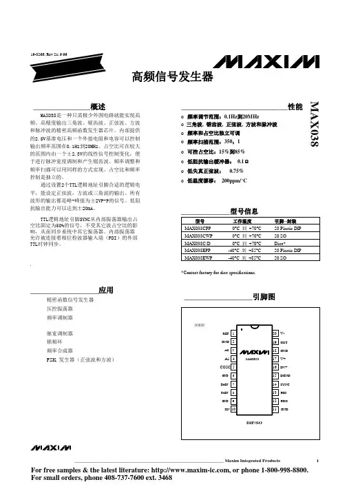
型号 MAX038CPP MAX038CWP MAX038C/D MAX038EPP MAX038EWP工作温度 0°C 到 +70°C 0°C 到 +70°C 0°C 到 +70°C -40°C 到 +85°C -40°C 到 +85°C引脚--封装 20 Plastic DIP 20 SO Dice* 20 Plastic DIP 20 SO.__________________应用精密函数信号发生器 压控振荡器 频率调制器*Contact factory for dice specifications.__________________引脚图脉宽调制器 锁相环 频率合成器FSK 发生器(正弦波和方波)________________________________________________________________ Maxim Integrated Products1For free samples & the latest literature: , or phone 1-800-998-8800. For small orders, phone 408-737-7600 ext. 3468MAX038高频信号发生器图1. 内部结构及基本工作电路_______________ 详细说明MAX038是一种高频函数信号发生器,它可以使 用最少的外部元件而产生低失真正弦波,三角波, 锯齿波,方波(脉冲波)。

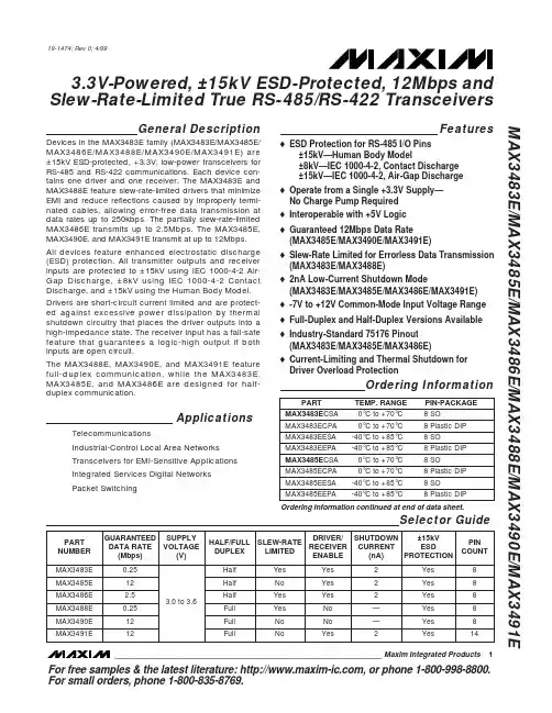
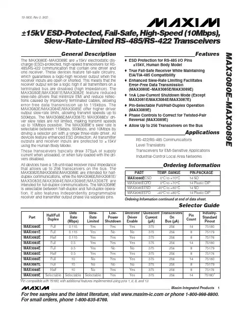
General DescriptionDevices in the MAX3483E family (MAX3483E/MAX3485E/MAX3486E/MAX3488E/MAX3490E/MAX3491E) are ±15kV ESD-protected, +3.3V, low-power transceivers for RS-485 and RS-422 communications. Each device con-tains one driver and one receiver. The MAX3483E and MAX3488E feature slew-rate-limited drivers that minimize EMI and reduce reflections caused by improperly termi-nated cables, allowing error-free data transmission at data rates up to 250kbps. The partially slew-rate-limited MAX3486E transmits up to 2.5Mbps. The MAX3485E,MAX3490E, and MAX3491E transmit at up to 12Mbps.All devices feature enhanced electrostatic discharge (ESD) protection. All transmitter outputs and receiver inputs are protected to ±15kV using IEC 1000-4-2 Air-Gap Discharge, ±8kV using IEC 1000-4-2 Contact Discharge, and ±15kV using the Human Body Model.Drivers are short-circuit current limited and are protect-ed against excessive power dissipation by thermal shutdown circuitry that places the driver outputs into a high-impedance state. The receiver input has a fail-safe feature that guarantees a logic-high output if both inputs are open circuit.The MAX3488E, MAX3490E, and MAX3491E feature full-duplex communication, while the MAX3483E,MAX3485E, and MAX3486E are designed for half-duplex communication.ApplicationsTelecommunicationsIndustrial-Control Local Area Networks Transceivers for EMI-Sensitive Applications Integrated Services Digital Networks Packet SwitchingFeatureso ESD Protection for RS-485 I/O Pins±15kV—Human Body Model±8kV—IEC 1000-4-2, Contact Discharge ±15kV—IEC 1000-4-2, Air-Gap Discharge o Operate from a Single +3.3V Supply—No Charge Pump Required o Interoperable with +5V Logic o Guaranteed 12Mbps Data Rate (MAX3485E/MAX3490E/MAX3491E)o Slew-Rate Limited for Errorless Data Transmission (MAX3483E/MAX3488E) o 2nA Low-Current Shutdown Mode(MAX3483E/MAX3485E/MAX3486E/MAX3491E)o -7V to +12V Common-Mode Input Voltage Range o Full-Duplex and Half-Duplex Versions Available o Industry-Standard 75176 Pinout (MAX3483E/MAX3485E/MAX3486E)o Current-Limiting and Thermal Shutdown for Driver Overload ProtectionMAX3483E/MAX3485E/MAX3486E/MAX3488E/MAX3490E/MAX3491E3.3V-Powered, ±15kV ESD-Protected, 12Mbps and Slew-Rate-Limited T rue RS-485/RS-422 T ransceivers________________________________________________________________Maxim Integrated Products119-1474; Rev 0; 4/99Selector GuideOrdering InformationOrdering Information continued at end of data sheet.For free samples & the latest literature: , or phone 1-800-998-8800.For small orders, phone 1-800-835-8769.M A X 3483E /M A X 3485E /M A X 3486E /M A X 3488E /M A X 3490E /M A X 3491E3.3V-Powered, ±15kV ESD-Protected, 12Mbps and Slew-Rate-Limited T rue RS-485/RS-422 T ransceiversABSOLUTE MAXIMUM RATINGSDC ELECTRICAL CHARACTERISTICS(V = +3.3V ±0.3V, T = T to T , unless otherwise noted. Typical values are at T = +25°C.)Stresses beyond those listed under “Absolute Maximum Ratings” may cause permanent damage to the device. These are stress ratings only, and functional operation of the device at these or any other conditions beyond those indicated in the operational sections of the specifications is not implied. Exposure to absolute maximum rating conditions for extended periods may affect device reliability.Supply Voltage (V CC ).............................................................+7V Control Input Voltage (RE , DE).................................-0.3V to +7V Driver Input Voltage (DI)...........................................-0.3V to +7V Driver Output Voltage (A, B, Y, Z).......................-7.5V to +12.5V Receiver Input Voltage (A, B)..............................-7.5V to +12.5V Receiver Output Voltage (RO)....................-0.3V to (V CC + 0.3V)Continuous Power Dissipation (T A = +70°C)8-Pin SO (derate 5.88mW/°C above +70°C)..................471mW 8-Pin Plastic DIP (derate 9.09mW/°C above +70°C).....727mW14-Pin SO (derate 8.33mW/°C above +70°C)................667mW 14-Pin Plastic DIP (derate 10mW/°C above +70°C)......800mW Operating Temperature RangesMAX34_ _ EC_ _...................................................0°C to +70°C MAX34_ _ EE_ _.................................................-40°C to +85°C Storage Temperature Range.............................-65°C to +150°C Lead Temperature (soldering, 10sec).............................+300°CMAX3483E/MAX3485E/MAX3486E/MAX3488E/MAX3490E/MAX3491E3.3V-Powered, ±15kV ESD-Protected, 12Mbps and Slew-Rate-Limited T rue RS-485/RS-422 T ransceiversDC ELECTRICAL CHARACTERISTICS (continued)(V CC = +3.3V ±0.3V, T A = T MIN to T MAX , unless otherwise noted. Typical values are at T A = +25°C.)DRIVER SWITCHING CHARACTERISTICS—MAX3485E/MAX3490E/MAX3491E(V = +3.3V, T = +25°C.)DRIVER SWITCHING CHARACTERISTICS—MAX3486E(V = +3.3V, T = +25°C.)*MAX3488E and MAX3491E will be compliant to ±8kV per IEC 1000-4-2 Contact Discharge by September 1999.M A X 3483E /M A X 3485E /M A X 3486E /M A X 3488E /M A X 3490E /M A X 3491E3.3V-Powered, ±15kV ESD-Protected, 12Mbps and Slew-Rate-Limited T rue RS-485/RS-422 T ransceivers4_______________________________________________________________________________________DRIVER SWITCHING CHARACTERISTICS—MAX3483E/MAX3488E(V CC = +3.3V, T A = +25°C.)RECEIVER SWITCHING CHARACTERISTICS(V CC = +3.3V, T A = +25°C.)Note 1:∆V OD and ∆V OC are the changes in V OD and V OC , respectively, when the DI input changes state.Note 2:Measured on |t PLH (Y) - t PHL (Y)|and |t PLH (Z) - t PHL (Z)|.Note 3:The transceivers are put into shutdown by bringing RE high and DE low. If the inputs are in this state for less than 80ns, thedevices are guaranteed not to enter shutdown. If the inputs are in this state for at least 300ns, the devices are guaranteed to have entered shutdown. See Low-Power Shutdown Mode section.MAX3483E/MAX3485E/MAX3486E/MAX3488E/MAX3490E/MAX3491E3.3V-Powered, ±15kV ESD-Protected, 12Mbps and Slew-Rate-Limited T rue RS-485/RS-422 T ransceivers_______________________________________________________________________________________5Typical Operating Characteristics(V CC = +3.3V, T A = +25°C, unless otherwise noted.)252015105000.51.01.52.02.53.53.0OUTPUT CURRENT vs.RECEIVER OUTPUT LOW VOLTAGEM A X 3483E -01OUTPUT LOW VOLTAGE (V)O U T P U T C U R R E N T (m A )-20-18-16-14-12-10-8-6-4-2000.51.01.52.02.53.53.0OUTPUT CURRENT vs.RECEIVER OUTPUT HIGH VOLTAGEM A X 3483E -02OUTPUT HIGH VOLTAGE (V)O U T P U T C U R R E N T (m A )3.003.053.103.153.203.253.30-40-20020406010080RECEIVER OUTPUT HIGH VOLTAGEvs. TEMPERATURETEMPERATURE (°C)O U T P U T H I G H V O L T A G E (V )00.10.20.30.40.50.60.70.8-40-2020406010080RECEIVER OUTPUT LOW VOLTAGEvs. TEMPERATURETEMPERATURE (°C)O U T P U T L O W V O L T A G E (V )2505075100125150175024681012OUTPUT CURRENT vs.DRIVER OUTPUT LOW VOLTAGEM A X 3483E -07OUTPUT LOW VOLTAGE (V)O U T P U T C U R R E N T (m A )100908070605040302010000.5 1.0 1.5 2.0 2.5 3.53.0DRIVER OUTPUT CURRENT vs.DIFFERENTIAL OUTPUT VOLTAGEM A X 3483E -05DIFFERENTIAL OUTPUT VOLTAGE (V)O U T P U T C U R R E N T (m A )1.61.71.81.92.02.12.22.32.42.62.5-40-20020406010080DRIVER DIFFERENTIAL OUTPUT VOLTAGE vs. TEMPERATURETEMPERATURE (°C)D I F FE R E N T I A L O U T P U T V O L T A G E (V )-100-80-60-40-20543210-7-6-3-4-5-2-1OUTPUT CURRENT vs.DRIVER OUTPUT HIGH VOLTAGEM A X 3483E -08OUTPUT HIGH VOLTAGE (V)O U T P U T C U R R E N T (m A )M A X 3483E /M A X 3485E /M A X 3486E /M A X 3488E /M A X 3490E /M A X 3491E3.3V-Powered, ±15kV ESD-Protected, 12Mbps and Slew-Rate-Limited T rue RS-485/RS-422 T ransceivers0.80.70.91.01.11.2-40-2020406010080SUPPLY CURRENT vs. TEMPERATURETEMPERATURE (°C)S U P P L Y C U R R E N T (m A )Typical Operating Characteristics (continued)(V CC = +3.3V, T A = +25°C, unless otherwise noted.)0102030405060708010090-40-2020406010080SHUTDOWN CURRENT vs. TEMPERATUREM A X 3483E -10TEMPERATURE (°C)S H U T D O W N C U R R E N T (n A )Pin DescriptionMAX3483E/MAX3485E/MAX3486E/MAX3488E/MAX3490E/MAX3491E3.3V-Powered, ±15kV ESD-Protected, 12Mbps and Slew-Rate-Limited T rue RS-485/RS-422 T ransceivers_______________________________________________________________________________________7Figure 2. MAX3488E/MAX3490E Pin Configuration and Typical Operating CircuitFigure 3. MAX3491E Pin Configuration and Typical Operating CircuitFigure 1. MAX3483E/MAX3485E/MAX3486E Pin Configuration and Typical Operating CircuitM A X 3483E /M A X 3485E /M A X 3486E /M A X 3488E /M A X 3490E /M A X 3491E3.3V-Powered, ±15kV ESD-Protected, 12Mbps and Slew-Rate-Limited T rue RS-485/RS-422 T ransceivers8_______________________________________________________________________________________Figure 4. Driver V OD and V OC Figure 7. Driver Differential Output Delay and Transition TimesFigure 6. Receiver V OH and V OLFigure 5. Driver V OD with Varying Common-Mode VoltageMAX3483E/MAX3485E/MAX3486E/MAX3488E/MAX3490E/MAX3491E3.3V-Powered, ±15kV ESD-Protected, 12Mbps and Slew-Rate-Limited T rue RS-485/RS-422 T ransceivers_______________________________________________________________________________________9Figure 8. Driver Propagation TimesFigure 9. Driver Enable and Disable Times (t PZH , t PSH , t PHZ )Figure 10. Driver Enable and Disable Times (t PZL , t PSL , t PLZ )M A X 3483E /M A X 3485E /M A X 3486E /M A X 3488E /M A X 3490E /M A X 3491E3.3V-Powered, ±15kV ESD-Protected, 12Mbps and Slew-Rate-Limited T rue RS-485/RS-422 T ransceivers10______________________________________________________________________________________Figure 11. Receiver Propagation DelayFigure 12. Receiver Enable and Disable TimesNote 4: The input pulse is supplied by a generator with the following characteristics: f = 250kHz, 50% duty cycle, t r ≤6.0ns, Z O = 50Ω.Note 5: C L includes probe and stray capacitance._____________________Function TablesDevices with Receiver/Driver Enable(MAX3483E/MAX3485E/MAX3486E/MAX3491E)Table 1. Transmitting* B and A outputs are Z and Y, respectively, for full-duplex part (MAX3491E).X = Don’t care; High-Z = High impedanceTable 2. Receiving* DE is a “don’t care” (x) for the full-duplex part (MAX3491E).X = Don’t care; High-Z = High impedanceDevices without Receiver/Driver Enable(MAX3488E/MAX3490E)Table 3. TransmittingTable 4. Receiving___________Applications InformationThe MAX3483E/MAX3485E/MAX3486E/MAX3488E/MAX3490E/MAX3491E are low-power transceivers for RS-485 and RS-422 communications. The MAX3483E and MAX3488E can transmit and receive at data rates up to 250kbps, the MAX3486E at up to 2.5Mbps, and the MAX3485E/MAX3490E/MAX3491E at up to 12Mbps. The MAX3488E/MAX3490E/MAX3491E are full-duplex trans-ceivers, while the MAX3483E/MAX3485E/MAX3486E are half-duplex. Driver Enable (DE) and Receiver Enable (RE ) pins are included on the MAX3483E/MAX3485E/MAX3486E/MAX3491E. When disabled, the driver and receiver outputs are high impedance.Reduced EMI and Reflections (MAX3483E/MAX3486E/MAX3488E)The MAX3483E/MAX3488E are slew-rate limited, mini-mizing EMI and reducing reflections caused by improp-erly terminated cables. Figure 13 shows the driver output waveform of a MAX3485E/MAX3490E/MAX3491E transmitting a 125kHz signal, as well as the Fourier analysis of that waveform. High-frequency harmonics with large amplitudes are evident. Figure 14 shows the same information, but for the slew-rate-limited MAX3483E/MAX3488E transmitting the same signal. The high-frequency harmonics have much lower amplitudes,and the potential for EMI is significantly reduced.Low-Power Shutdown Mode(MAX3483E/MAX3485E/MAX3486E/MAX3491E)A low-power shutdown mode is initiated by bringing both RE high and DE low. The devices will not shut down unless both the driver and receiver are disabled (high impedance). In shutdown, the devices typically draw only 2nA of supply current.For these devices, the t PSH and t PSL enable times assume the part was in the low-power shutdown mode;the t PZH and t PZL enable times assume the receiver or driver was disabled, but the part was not shut down.MAX3483E/MAX3485E/MAX3486E/MAX3488E/MAX3490E/MAX3491E3.3V-Powered, ±15kV ESD-Protected, 12Mbps and Slew-Rate-Limited T rue RS-485/RS-422 T ransceivers______________________________________________________________________________________11INPUTS OUTPUT A, B RO ≥+0.2V 1≤-0.2V 0Inputs Open1INPUT OUTPUTS DI Z Y 101015MHz 500kHz/div 05MHz500kHz/div Figure 13. Driver Output Waveform and FFT Plot of MAX3485E/MAX3490E/MAX3491E Transmitting a 125kHz Signal Figure 14. Driver Output Waveform and FFT Plot of MAX3483E/ MAX3488E Transmitting a 125kHz SignalM A X 3483E /M A X 3485E /M A X 3486E /M A X 3488E /M A X 3490E /M A X 3491E3.3V-Powered, ±15kV ESD-Protected, 12Mbps and Slew-Rate-Limited T rue RS-485/RS-422 T ransceivers12______________________________________________________________________________________Figure 17. MAX3483E/MAX3488E Driver Propagation Delay Figure 19. MAX3483E/MAX3488E System Differential Voltage at 125kHz Driving 4000 Feet of Cable Figure 20. MAX3485E/MAX3490E/MAX3491E System Differential Voltage at 125kHz Driving 4000 Feet of CableDriver-Output Protection Excessive output current and power dissipation caused by faults or by bus contention are prevented by two mechanisms. A foldback current limit on the output stage provides immediate protection against short circuits over the whole common-mode voltage range (see Typical Operating Characteristics). In addition, a thermal shut-down circuit forces the driver outputs into a high-imped-ance state if the die temperature rises excessively.Propagation Delay Figures 15–18 show the typical propagation delays. Skew time is simply the difference between the low-to-high and high-to-low propagation delay. Small driver/receiver skew times help maintain a symmetrical mark-space ratio (50% duty cycle).The receiver skew time, |t PRLH- t PRHL|, is under 10ns (20ns for the MAX3483E/MAX3488E). The driver skew times are 8ns for the MAX3485E/MAX3490E/MAX3491E, 12ns for the MAX3486E, and typically under 50ns for the MAX3483E/MAX3488E.Line Length vs. Data Rate The RS-485/RS-422 standard covers line lengths up to 4000 feet. For line lengths greater than 4000 feet, see Figure 21 for an example of a line repeater.Figures 19 and 20 show the system differential voltage for parts driving 4000 feet of 26AWG twisted-pair wire at 125kHz into 120Ωloads.For faster data rate transmission, please consult the fac-tory.±15kV ESD Protection As with all Maxim devices, ESD-protection structures are incorporated on all pins to protect against electrostatic discharges encountered during handling and assembly. The driver outputs and receiver inputs of the MAX3483E family of devices have extra protection against static electricity. Maxim’s engineers have developed state-of-the-art structures to protect these pins against ESD of ±15kV without damage. The ESD structures withstand high ESD in all states: normal operation, shutdown, and powered down. After an ESD event, Maxim’s E versions keep working without latchup or damage.ESD protection can be tested in various ways; the transmitter outputs and receiver inputs of this product family are characterized for protection to the following limits:1)±15kV using the Human Body Model2)±8kV using the Contact-Discharge method specifiedin IEC 1000-4-23)±15kV using IEC 1000-4-2’s Air-Gap method.ESD Test Conditions ESD performance depends on a variety of conditions. Contact Maxim for a reliability report that documents test setup, test methodology, and test results.Human Body Model Figure 22a shows the Human Body Model and Figure 22b shows the current waveform it generates when dis-charged into a low impedance. This model consists of a 100pF capacitor charged to the ESD voltage of inter-est, which is then discharged into the test device through a 1.5kΩresistor.IEC 1000-4-2 The IEC 1000-4-2 standard covers ESD testing and performance of finished equipment; it does not specifi-cally refer to integrated circuits. The MAX3483E family of devices helps you design equipment that meets Level 4 (the highest level) of IEC 1000-4-2, without the need for additional ESD-protection components.The major difference between tests done using the Human Body Model and IEC 1000-4-2 is higher peak current in IEC 1000-4-2, because series resistance is lower in the IEC 1000-4-2 model. Hence, the ESD with-stand voltage measured to IEC 1000-4-2 is generally lower than that measured using the Human Body Model. Figure 23a shows the IEC 1000-4-2 model, and Figure 23b shows the current waveform for the ±8kV IEC 1000-4-2, Level 4 ESD contact-discharge test.Figure 21. Line Repeater for MAX3488E/MAX3490E/MAX3491EMAX3483E/MAX3485E/MAX3486E/MAX3488E/MAX3490E/MAX3491E3.3V-Powered, ±15kV ESD-Protected, 12Mbps and Slew-Rate-Limited T rue RS-485/RS-422 T ransceivers ______________________________________________________________________________________13M A X 3483E /M A X 3485E /M A X 3486E /M A X 3488E /M A X 3490E /M A X 3491EThe air-gap test involves approaching the device with a charged probe. The contact-discharge method connects the probe to the device before the probe is energized.Machine ModelThe Machine Model for ESD tests all pins using a 200pF storage capacitor and zero discharge resis-tance. Its objective is to emulate the stress caused when I/O pins are contacted by handling equipment during test and assembly. Of course, all pins require this protection, not just RS-485 inputs and outputs.Typical ApplicationsThe MAX3483E/MAX3485E/MAX3486E/MAX3488E/MAX3490E/MAX3491E transceivers are designed for bidirectional data communications on multipoint bus transmission lines. Figures 24 and 25 show typical net-work applications circuits. These parts can also be used as line repeaters, with cable lengths longer than 4000 feet, as shown in Figure 21.To minimize reflections, the line should be terminated at both ends in its characteristic impedance, and stub lengths off the main line should be kept as short as possible. The slew-rate-limited MAX3483E/MAX3488E and the partially slew-rate-limited MAX3486E are more tolerant of imperfect termination.3.3V-Powered, ±15kV ESD-Protected, 12Mbps and Slew-Rate-Limited T rue RS-485/RS-422 T ransceivers14______________________________________________________________________________________Figure 22a. Human Body ESD Test ModelFigure 22b. Human Body Current WaveformFigure 23a. IEC 1000-4-2 ESD Test ModelFigure 23b. IEC 1000-4-2 ESD Generator Current WaveformMAX3483E/MAX3485E/MAX3486E/MAX3488E/MAX3490E/MAX3491E3.3V-Powered, ±15kV ESD-Protected, 12Mbps and Slew-Rate-Limited T rue RS-485/RS-422 T ransceivers______________________________________________________________________________________15Figure 25. MAX3488E/MAX3490E/MAX3491E Full-Duplex RS-485 NetworkFigure 24. MAX3483E/MAX3485E/MAX3486E Typical RS-485 NetworkM A X 3483E /M A X 3485E /M A X 3486E /M A X 3488E /M A X 3490E /M A X 3491E3.3V-Powered, ±15kV ESD-Protected, 12Mbps and Slew-Rate-Limited T rue RS-485/RS-422 T ransceiversTRANSISTOR COUNT: 761Chip InformationOrdering Information (continued)Maxim cannot assume responsibility for use of any circuitry other than circuitry entirely embodied in a Maxim product. No circuit patent licenses are implied. Maxim reserves the right to change the circuitry and specifications without notice at any time.16____________________Maxim Integrated Products, 120 San Gabriel Drive, Sunnyvale, CA 94086 408-737-7600©1999 Maxim Integrated ProductsPrinted USAis a registered trademark of Maxim Integrated Products.。
General DescriptionThe MAX3311E/MAX3313E are low-power, 5V EIA/TIA-232-compatible transceivers. All transmitter outputs and receiver inputs are protected to ±15kV using the Human Body Model, making these devices ideal for applications where more robust transceivers are required.Both devices have one transmitter and one receiver.The transmitters have a proprietary low-dropout trans-mitter output stage enabling RS-232-compatible opera-tion from a +5V supply with a single inverting charge pump. These transceivers require only three 0.1µF capacitors and will run at data rates up to 460kbps while maintaining RS-232-compatible output levels.The MAX3311E features a 1µA shutdown mode. In shutdown the device turns off the charge pump, pulls V- to ground, and the transmitter output is disabled.The MAX3313E features an INVALID output that asserts high when an active RS-232 cable signal is connected,signaling to the host that a peripheral is connected to the communication port.________________________ApplicationsDigital Cameras PDAs GPS POSTelecommunications Handy Terminals Set-Top BoxesFeatureso ESD Protection for RS-232-Compatible I/O Pins±15kV—Human Body Modelo 1µA Low-Power Shutdown (MAX3311E)o INVALID Output (MAX3313E)o Receiver Active in Shutdown (MAX3311E)o Single Transceiver (1Tx/1Rx) in 10-Pin µMAX PackageMAX3311E/MAX3313E±15kV ESD-Protected, 460kbps, 1µA,RS-232-Compatible Transceivers in µMAX________________________________________________________________Maxim Integrated Products1Pin Configurations19-1910; Rev 0; 1/01Ordering InformationFor price, delivery, and to place orders,please contact Maxim Distribution at 1-888-629-4642,or visit Maxim’s website at .Typical Operating CircuitM A X 3311E /M A X 3313E±15kV ESD-Protected, 460kbps, 1µA,RS-232-Compatible Transceivers in µMAX 2_______________________________________________________________________________________ABSOLUTE MAXIMUM RATINGSELECTRICAL CHARACTERISTICSStresses beyond those listed under “Absolute Maximum Ratings” may cause permanent damage to the device. These are stress ratings only, and functional operation of the device at these or any other conditions beyond those indicated in the operational sections of the specifications is not implied. Exposure to absolute maximum rating conditions for extended periods may affect device reliability.V CC to GND.............................................................-0.3V to +6V V- to GND................................................................+0.3V to -7V V CC + |V-|............................................................................+13V Input VoltagesTIN, SHDN to GND...............................................-0.3V to +6V RIN to GND......................................................................±25V Output VoltagesTOUT to GND................................................................±13.2V ROUT, INVALID to GND.....................…-0.3V to (V CC + 0.3V)Short-Circuit DurationTOUT to GND.........................................................ContinuousContinuous Power Dissipation10-Pin µMAX (derate 5.6mW/°C above +70°C)..........444mW Operating Temperature RangesMAX331_ECUB.................................................0°C to +70°C MAX331_EEUB..............................................-40°C to +85°C Junction Temperature.....................................................+150°C Storage Temperature Range............................-65°C to +150°C Lead Temperature (soldering, 10s)................................+300°CMAX3311E/MAX3313E±15kV ESD-Protected, 460kbps, 1µA,RS-232-Compatible Transceivers in µMAX_______________________________________________________________________________________3ELECTRICAL CHARACTERISTICS (continued)TIMING CHARACTERISTICSM A X 3311E /M A X 3313E±15kV ESD-Protected, 460kbps, 1µA,RS-232-Compatible Transceivers in µMAX 4_______________________________________________________________________________________Typical Operating Characteristics(V CC = +5V, 0.1µF capacitors, transmitter loaded with 3k Ωand C L , T A = +25°C, unless otherwise noted.)0428612101410001500500200025003000SLEW RATEvs. LOAD CAPACITANCELOAD CAPACITANCE (pF)S L E W R A T E (V /µs )-5-4-3-2-10123456050010001500200025003000TRANSMITTER OUTPUT VOLTAGEvs. LOAD CAPACITANCELOAD CAPACITANCE (pF)T R A N S M I T T E R O U T P U T V O L T A G E (V )010001500500200025003000SUPPLY CURRENT vs. LOAD CAPACITANCELOAD CAPACITANCE (pF)Detailed DescriptionSingle Charge-Pump Voltage ConverterThe MAX3311E/MAX3313E internal power supply has a single inverting charge pump that provides a negative voltage from a single +5V supply. The charge pump operates in a discontinuous mode and requires a flying capacitor (C1) and a reservoir capacitor (C2) to gener-ate the V- supply.RS-232-Compatible DriverThe transmitter is an inverting level translator that con-verts CMOS-logic levels to EIA/TIA-232 compatible lev-els. It guarantees data rates up to 460kbps with worst-case loads of 3k Ωin parallel with 1000pF. When SHDN is driven low, the transmitter is disabled and put into tri-state. The transmitter input does not have an internal pullup resistor.RS-232 ReceiverThe MAX3311E/MAX3313E receiver converts RS-232signals to CMOS-logic output levels. The MAX3311E receiver will remain active during shutdown mode. The MAX3313E INVALID indicates when an RS-232 signal is present at the receiver input, and therefore when the port is in use.The MAX3313E INVALID output is pulled low when no valid RS-232 signal level is detected on the receiver input.MAX3311E Shutdown ModeIn shutdown mode, the charge pump is turned off, V- is pulled to ground, and the transmitter output is disabled (Table 1). This reduces supply current typically to 1µA.The time required to exit shutdown is less than 25ms.Applications InformationCapacitor SelectionThe capacitor type used for C1 and C2 is not critical for proper operation; either polarized or nonpolarized capacitors are acceptable. If polarized capacitors are used, connect polarity as shown in the Typical Operating Circuit . The charge pump requires 0.1µF capacitors. Increasing the capacitor values (e.g., by a factor of 2) reduces power consumption. C2 can beincreased without changing C1’s value. However, do not increase C1’s value without also increasing the value of C2 and C BYPASS to maintain the proper ratios (C1 to the other capacitors).When using the minimum 0.1µF capacitors, make sure the capacitance does not degrade excessively with temperature. If in doubt, use capacitors with a larger nominal value. The capacitor ’s equivalent series resis-tance (ESR) usually rises at low temperatures and influ-ences the amount of ripple on V-.To reduce the output impedance at V-, use larger capacitors (up to 10µF).Bypass V CC to ground with at least 0.1µF. In applica-tions sensitive to power-supply noise generated by the charge pump, decouple V CC to ground with a capaci-tor the same size as (or larger than) charge-pump capacitors C1 and C2.Transmitter Output when ExitingShutdownFigure 1 shows the transmitter output when exiting shutdown mode. The transmitter is loaded with 3k Ωin parallel with 1000pF. The transmitter output displays no ringing or undesirable transients as the MAX3311E comes out of shutdown. Note that the transmitter is enabled only when the magnitude of V- exceeds approximately -3V.High Data RatesThe MAX3311E/MAX3313E maintain RS-232-compati-ble ±3.7V minimum transmitter output voltage even atMAX3311E/MAX3313E±15kV ESD-Protected, 460kbps, 1µA,RS-232-Compatible Transceivers in µMAX5Figure 1. Transmitter Output when Exiting Shutdown or Powering Up10µs/divSHDNTOUT5V/div1.5V/divTIN = GNDTIN = V CCM A X 3311E /M A X 3313E±15kV ESD-Protected, 460kbps, 1µA,RS-232-Compatible Transceivers in µMAX 6_______________________________________________________________________________________high data rates. Figure 2 shows a transmitter loopback test circuit. Figure 3 shows the loopback test result at 120kbps, and Figure 4 shows the same test at 250kbps.±15kV ESD ProtectionAs with all Maxim devices, ESD-protection structures are incorporated on all pins to protect against electro-static discharges encountered during handling and assembly. The MAX3311E/MAX3313E driver outputsand receiver inputs have extra protection against static discharge. Maxim ’s engineers have developed state-of-the-art structures to protect these pins against ESD of ±15kV without damage. The ESD structures withstand high ESD in all states: normal operation, shutdown, and powered down. After an ESD event, Maxim ’s E versions keep working without latchup; whereas, competing products can latch and must be powered down to remove latchup.ESD protection can be tested in various ways. The transmitter outputs and receiver inputs of the product family are characterized for protection to ±15kV using the Human Body Model.ESD Test ConditionsESD performance depends on a variety of conditions.Contact Maxim for a reliability report that documents test setup, test methodology, and test results.Human Body ModelFigure 5 shows the Human Body Model, and Figure 6shows the current waveform it generates when dis-charged into low impedance. This model consists of a 100pF capacitor charged to the ESD voltage of interest,which is then discharged into the test device through a 1.5k Ωresistor.Machine ModelThe Machine Model for ESD tests all pins using a 200pF storage capacitor and zero discharge resis-tance. Its objective is to emulate the stress caused by contact that occurs with handling and assembly during manufacturing. Of course, all pins require this protec-tion during manufacturing, not just RS-232 inputs and outputs. Therefore, after PC board assembly, the Machine Model is less relevant to I/O ports.Figure 4. Loopback Test Results at 250kbps2µs/divTOUTTINROUTFigure 3. Loopback Test Results at 120kbps 5µs/divTOUTTINROUTMAX3311E/MAX3313E±15kV ESD-Protected, 460kbps, 1µA,RS-232-Compatible Transceivers in µMAX_______________________________________________________________________________________7Figure 5. Human Body ESD Test ModelFigure 6. Human Body Current WaveformPin Configurations (continued)Chip InformationTRANSISTOR COUNT: 278M A X 3311E /M A X 3313E±15kV ESD-Protected, 460kbps, 1µA,RS-232-Compatible Transceivers in µMAX Maxim cannot assume responsibility for use of any circuitry other than circuitry entirely embodied in a Maxim product. No circuit patent licenses are implied. Maxim reserves the right to change the circuitry and specifications without notice at any time.8_____________________Maxim Integrated Products, 120 San Gabriel Drive, Sunnyvale, CA 94086 408-737-7600©2001 Maxim Integrated ProductsPrinted USAis a registered trademark of Maxim Integrated Products.______________________________________________________________Pin Description。
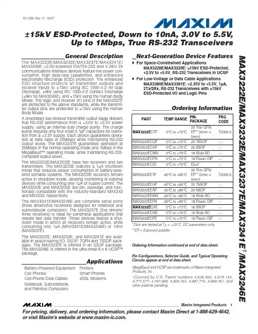
For pricing, delivery, and ordering information, please contact Maxim Direct at 1-888-629-4642,or visit Maxim's website at .General DescriptionThe MAX3222E/MAX3232E/MAX3237E/MAX3241E/MAX3246E +3.0V-powered EIA/TIA-232 and V.28/V.24communications interface devices feature low power con-sumption, high data-rate capabilities, and enhanced electrostatic-discharge (ESD) protection. The enhanced ESD structure protects all transmitter outputs and receiver inputs to ±15kV using IEC 1000-4-2 Air-G ap Discharge, ±8kV using IEC 1000-4-2 Contact Discharge (±9kV for MAX3246E), and ±15kV using the Human Body Model. The logic and receiver I/O pins of the MAX3237E are protected to the above standards, while the transmit-ter output pins are protected to ±15kV using the Human Body Model.A proprietary low-dropout transmitter output stage delivers true RS-232 performance from a +3.0V to +5.5V power supply, using an internal dual charge pump. The charge pump requires only four small 0.1µF capacitors for opera-tion from a +3.3V supply. Each device guarantees opera-tion at data rates of 250kbps while maintaining RS-232output levels. The MAX3237E guarantees operation at 250kbps in the normal operating mode and 1Mbps in the MegaBaud™ operating mode, while maintaining RS-232-compliant output levels.The MAX3222E/MAX3232E have two receivers and two transmitters. The MAX3222E features a 1µA shutdown mode that reduces power consumption in battery-pow-ered portable systems. The MAX3222E receivers remain active in shutdown mode, allowing monitoring of external devices while consuming only 1µA of supply current. The MAX3222E and MAX3232E are pin, package, and func-tionally compatible with the industry-standard MAX242and MAX232, respectively.The MAX3241E/MAX3246E are complete serial ports (three drivers/five receivers) designed for notebook and subnotebook computers. The MAX3237E (five drivers/three receivers) is ideal for peripheral applications that require fast data transfer. These devices feature a shut-down mode in which all receivers remain active, while consuming only 1µA (MAX3241E/MAX3246E) or 10nA (MAX3237E).The MAX3222E, MAX3232E, and MAX3241E are avail-able in space-saving SO, SSOP, TQFN and TSSOP pack-ages. The MAX3237E is offered in an SSOP package.The MAX3246E is offered in the ultra-small 6 x 6 UCSP™package.ApplicationsBattery-Powered Equipment PrintersCell PhonesSmart Phones Cell-Phone Data Cables xDSL ModemsNotebook, Subnotebook,and Palmtop ComputersNext-Generation Device Features♦For Space-Constrained ApplicationsMAX3228E/MAX3229E: ±15kV ESD-Protected, +2.5V to +5.5V, RS-232 Transceivers in UCSP ♦For Low-Voltage or Data Cable ApplicationsMAX3380E/MAX3381E: +2.35V to +5.5V, 1µA, 2Tx/2Rx, RS-232 Transceivers with ±15kV ESD-Protected I/O and Logic PinsMAX3222E/MAX3232E/MAX3237E/MAX3241E †/MAX3246E±15kV ESD-Protected, Down to 10nA, 3.0V to 5.5V ,Up to 1Mbps, True RS-232 Transceivers________________________________________________________________Maxim Integrated Products 119-1298; Rev 11; 10/07Ordering Information continued at end of data sheet.*Dice are tested at T A = +25°C, DC parameters only.**EP = Exposed paddle.Pin Configurations, Selector Guide, and Typical Operating Circuits appear at end of data sheet.MegaBaud and UCSP are trademarks of Maxim Integrated Products, Inc.†Covered by U.S. Patent numbers 4,636,930; 4,679,134;4,777,577; 4,797,899; 4,809,152; 4,897,774; 4,999,761; and other patents pending.M A X 3222E /M A X 3232E /M A X 3237E /M A X 3241E †/M A X 3246EUp to 1Mbps, True RS-232 TransceiversABSOLUTE MAXIMUM RATINGSELECTRICAL CHARACTERISTICS(V CC = +3V to +5.5V, C1–C4 = 0.1µF, T A = T MIN to T MAX , unless otherwise noted. Typical values are at T A = +25°C.) (Notes 3, 4)Stresses beyond those listed under “Absolute Maximum Ratings” may cause permanent damage to the device. These are stress ratings only, and functional operation of the device at these or any other conditions beyond those indicated in the operational sections of the specifications is not implied. Exposure to absolute maximum rating conditions for extended periods may affect device reliability.V CC to GND..............................................................-0.3V to +6V V+ to GND (Note 1)..................................................-0.3V to +7V V- to GND (Note 1)...................................................+0.3V to -7V V+ + |V-| (Note 1).................................................................+13V Input Voltages T_IN, EN , SHDN , MBAUD to GND ........................-0.3V to +6V R_IN to GND.....................................................................±25V Output Voltages T_OUT to GND...............................................................±13.2V R_OUT, R_OUTB (MAX3241E)................-0.3V to (V CC + 0.3V)Short-Circuit Duration, T_OUT to GND.......................Continuous Continuous Power Dissipation (T A = +70°C)16-Pin SSOP (derate 7.14mW/°C above +70°C)..........571mW 16-Pin TSSOP (derate 9.4mW/°C above +70°C).......754.7mW 16-Pin TQFN (derate 20.8mW/°C above +70°C).....1666.7mW 16-Pin Wide SO (derate 9.52mW/°C above +70°C).....762mW 18-Pin Wide SO (derate 9.52mW/°C above +70°C).....762mW 18-Pin PDIP (derate 11.11mW/°C above +70°C)..........889mW 20-Pin TQFN (derate 21.3mW/°C above +70°C)........1702mW 20-Pin TSSOP (derate 10.9mW/°C above +70°C)........879mW 20-Pin SSOP (derate 8.00mW/°C above +70°C)..........640mW 28-Pin SSOP (derate 9.52mW/°C above +70°C)..........762mW 28-Pin Wide SO (derate 12.50mW/°C above +70°C).............1W 28-Pin TSSOP (derate 12.8mW/°C above +70°C)......1026mW 32-Lead Thin QFN (derate 33.3mW/°C above +70°C)..2666mW 6 x 6 UCSP (derate 12.6mW/°C above +70°C).............1010mW Operating Temperature Ranges MAX32_ _EC_ _...................................................0°C to +70°C MAX32_ _EE_ _.................................................-40°C to +85°C Storage Temperature Range.............................-65°C to +150°C Lead Temperature (soldering, 10s).................................+300°C Bump Reflow Temperature (Note 2)Infrared, 15s..................................................................+200°C Vapor Phase, 20s..........................................................+215°C Note 1:V+ and V- can have maximum magnitudes of 7V, but their absolute difference cannot exceed 13V.Note 2:This device is constructed using a unique set of packaging techniques that impose a limit on the thermal profile the devicecan be exposed to during board-level solder attach and rework. This limit permits only the use of the solder profiles recom-mended in the industry-standard specification, JEDEC 020A, paragraph 7.6, Table 3 for IR/VPR and convection reflow.Preheating is required. Hand or wave soldering is not allowed.MAX3222E/MAX3232E/MAX3237E/MAX3241E †/MAX3246EUp to 1Mbps, True RS-232 Transceivers_______________________________________________________________________________________3M A X 3222E /M A X 3232E /M A X 3237E /M A X 3241E †/M A X 3246EUp to 1Mbps, True RS-232 Transceivers4_______________________________________________________________________________________TIMING CHARACTERISTICS—MAX3237E(V CC = +3V to +5.5V, C1–C4 = 0.1µF, T A = T MIN to T MAX , unless otherwise noted. Typical values are at T A = +25°C.) (Note 3)±10%. MAX3237E: C1–C4 = 0.1µF tested at +3.3V ±5%, C1–C4 = 0.22µF tested at +3.3V ±10%; C1 = 0.047µF, C2, C3, C4 =0.33µF tested at +5.0V ±10%. MAX3246E; C1-C4 = 0.22µF tested at +3.3V ±10%; C1 = 0.22µF, C2, C3, C4 = 0.54µF tested at 5.0V ±10%.Note 4:MAX3246E devices are production tested at +25°C. All limits are guaranteed by design over the operating temperature range.Note 5:The MAX3237E logic inputs have an active positive feedback resistor. The input current goes to zero when the inputs are atthe supply rails.Note 6:MAX3241EEUI is specified at T A = +25°C.Note 7:Transmitter skew is measured at the transmitter zero crosspoints.TIMING CHARACTERISTICS—MAX3222E/MAX3232E/MAX3241E/MAX3246EMAX3222E/MAX3232E/MAX3237E/MAX3241E †/MAX3246EUp to 1Mbps, True RS-232 Transceivers_______________________________________________________________________________________5-6-4-202460MAX3237ETRANSMITTER OUTPUT VOLTAGE vs. LOAD CAPACITANCE (MBAUD = GND)LOAD CAPACITANCE (pF)T R A N S M I T T E R O U T P U T V O L T A G E (V )10001500500200025003000531-1-3-5-6-2-42046-5-31-135010001500500200025003000LOAD CAPACITANCE (pF)T R A N S M I T T E R O U T P U T V O L T A G E (V )MAX3237ETRANSMITTER OUTPUT VOLTAGEvs. LOAD CAPACITANCE-7.5-5.0-2.502.55.07.5MAX3237ETRANSMITTER OUTPUT VOLTAGE vs. LOAD CAPACITANCE (MBAUD = V CC )LOAD CAPACITANCE (pF)T R A N S M I T T E R O U T P U T V O L T A G E (V )500100015002000__________________________________________Typical Operating Characteristics(V CC = +3.3V, 250kbps data rate, 0.1µF capacitors, all transmitters loaded with 3k Ωand C L , T A = +25°C, unless otherwise noted.)-6-5-4-3-2-10123456010002000300040005000MAX3241ETRANSMITTER OUTPUT VOLTAGEvs. LOAD CAPACITANCELOAD CAPACITANCE (pF)T R A N S M I T T E R O U T P U T V O L T A G E (V)302010405060020001000300040005000MAX3241EOPERATING SUPPLY CURRENT vs. LOAD CAPACITANCELOAD CAPACITANCE (pF)S U P P L Y C U R R E N T (m A )04286121014010002000300040005000MAX3241ESLEW RATE vs. LOAD CAPACITANCEM A X 3237E t o c 05LOAD CAPACITANCE (pF)S L E W R A T E (V /μs )-6-5-4-3-2-10123456010002000300040005000MAX3222E/MAX3232ETRANSMITTER OUTPUT VOLTAGEvs. LOAD CAPACITANCELOAD CAPACITANCE (pF)T R A N S M I T T E R O U T P UT V O L T A G E (V )624108141216010002000300040005000MAX3222E/MAX3232ESLEW RATE vs. LOAD CAPACITANCELOAD CAPACITANCE (pF)S L E W R A T E (V /μs)2520155103530404520001000300040005000MAX3222E/MAX3232E OPERATING SUPPLY CURRENT vs. LOAD CAPACITANCELOAD CAPACITANCE (pF)S U P P L Y C U R R E N T (m A )M A X 3222E /M A X 3232E /M A X 3237E /M A X 3241E †/M A X 3246EUp to 1Mbps, True RS-232 Transceivers6_______________________________________________________________________________________Typical Operating Characteristics (continued)(V CC = +3.3V, 250kbps data rate, 0.1µF capacitors, all transmitters loaded with 3k Ωand C L , T A = +25°C, unless otherwise noted.)20604080100MAX3237ETRANSMITTER SKEW vs. LOAD CAPACITANCE(MBAUD = V CC )LOAD CAPACITANCE (pF)100015005002000T R A N S M I T T E R S K E W (n s )-6-2-42046-3-51-1352.03.03.52.54.04.55.0SUPPLY VOLTAGE (V)T R A N S M I T T E R O U T P U T V O L T A G E (V )MAX3237ETRANSMITTER OUTPUT VOLTAGE vs. SUPPLY VOLTAGE (MBAUD = GND)10203040502.0MAX3237E SUPPLY CURRENT vs. SUPPLY VOLTAGE (MBAUD = GND)SUPPLY VOLTAGE (V)S U P P L Y C U R R E N T (m A )3.03.52.54.04.55.0MAX3246ETRANSMITTER OUTPUT VOLTAGEvs. LOAD CAPACITANCELOAD CAPACITANCE (pF)T R A N S M I T T E R O U T P U T V O L T A G E (V )4000300010002000-5-4-3-2-101234567-65000468101214160MAX3246ESLEW RATE vs. LOAD CAPACITANCELOAD CAPACITANCE (pF)S L EW R A T E (V /μs )200030001000400050001020304050600MAX3246EOPERATING SUPPLY CURRENT vs. LOAD CAPACITANCEM A X 3237E t o c 17LOAD CAPACITANCE (pF)S U P P L Y C U R R EN T (m A )1000200030004000500055453525155024681012MAX3237ESLEW RATE vs. LOAD CAPACITANCE(MBAUD = GND)LOAD CAPACITANCE (pF)S L E W R A T E (V /μs )10001500500200025003000010203050406070MAX3237ESLEW RATE vs. LOAD CAPACITANCE(MBAUD = V CC )LOAD CAPACITANCE (pF)S L E W R A T E (V /μs )5001000150020001020304050MAX3237ESUPPLY CURRENT vs. LOAD CAPACITANCE WHEN TRANSMITTING DATA (MBAUD = GND)LOAD CAPACITANCE (pF)S U P P L Y C U R R E N T (m A )10001500500200025003000MAX3222E/MAX3232E/MAX3237E/MAX3241E †/MAX3246EUp to 1Mbps, True RS-232 Transceivers_______________________________________________________________________________________7Pin DescriptionM A X 3222E /M A X 3232E /M A X 3237E /M A X 3241E †/M A X 3246EUp to 1Mbps, True RS-232 Transceivers8_______________________________________________________________________________________MAX3222E/MAX3232E/MAX3237E/MAX3241E †/MAX3246EUp to 1Mbps, True RS-232 Transceivers_______________________________________________________________________________________9Detailed DescriptionDual Charge-Pump Voltage ConverterThe MAX3222E/MAX3232E/MAX3237E/MAX3241E/MAX3246Es’ internal power supply consists of a regu-lated dual charge pump that provides output voltages of +5.5V (doubling charge pump) and -5.5V (inverting charge pump) over the +3.0V to +5.5V V CC range. The charge pump operates in discontinuous mode; if the output voltages are less than 5.5V, the charge pump is enabled, and if the output voltages exceed 5.5V, the charge pump is disabled. Each charge pump requires a flying capacitor (C1, C2) and a reservoir capacitor (C3, C4) to generate the V+ and V- supplies (Figure 1).RS-232 TransmittersThe transmitters are inverting level translators that con-vert TTL/CMOS-logic levels to ±5V EIA/TIA-232-compli-ant levels.The MAX3222E/MAX3232E/MAX3237E/MAX3241E/MAX3246E transmitters guarantee a 250kbps data rate with worst-case loads of 3k Ωin parallel with 1000pF,providing compatibility with PC-to-PC communication software (such as LapLink™). Transmitters can be par-alleled to drive multiple receivers or mice.The MAX3222E/MAX3237E/MAX3241E/MAX3246E transmitters are disabled and the outputs are forcedinto a high-impedance state when the device is in shut-down mode (SHDN = G ND). The MAX3222E/MAX3232E/MAX3237E/MAX3241E/MAX3246E permit the outputs to be driven up to ±12V in shutdown.The MAX3222E/MAX3232E/MAX3241E/MAX3246E transmitter inputs do not have pullup resistors. Connect unused inputs to GND or V CC . The MAX3237E’s trans-mitter inputs have a 400k Ωactive positive-feedback resistor, allowing unused inputs to be left unconnected.MAX3237E MegaBaud OperationFor higher-speed serial communications, the MAX3237E features MegaBaud operation. In MegaBaud operating mode (MBAUD = V CC ), the MAX3237E transmitters guarantee a 1Mbps data rate with worst-case loads of 3k Ωin parallel with 250pF for +3.0V < V CC < +4.5V. For +5V ±10% operation, the MAX3237E transmitters guarantee a 1Mbps data rate into worst-case loads of 3k Ωin parallel with 1000pF.RS-232 ReceiversThe receivers convert RS-232 signals to CMOS-logic output levels. The MAX3222E/MAX3237E/MAX3241E/MAX3246E receivers have inverting three-state outputs.Drive EN high to place the receiver(s) into a high-impedance state. Receivers can be either active or inactive in shutdown (Table 1).Figure 1. Slew-Rate Test CircuitsLapLink is a trademark of Traveling Software.M A X 3222E /M A X 3232E /M A X 3237E /M A X 3241E †/M A X 3246EUp to 1Mbps, True RS-232 Transceivers10______________________________________________________________________________________The complementary outputs on the MAX3237E/MAX3241E (R_OUTB) are always active, regardless of the state of EN or SHDN . This allows the device to be used for ring indicator applications without forward biasing other devices connected to the receiver outputs. This is ideal for systems where V CC drops to zero in shutdown to accommodate peripherals such as UARTs (Figure 2).MAX3222E/MAX3237E/MAX3241E/MAX3246E Shutdown ModeSupply current falls to less than 1µA in shutdown mode (SHDN = low). The MAX3237E’s supply current falls to10nA (typ) when all receiver inputs are in the invalid range (-0.3V < R_IN < +0.3). When shut down, the device’s charge pumps are shut off, V+ is pulled down to V CC , V- is pulled to ground, and the transmitter out-puts are disabled (high impedance). The time required to recover from shutdown is typically 100µs, as shown in Figure 3. Connect SHDN to V CC if shutdown mode is not used. SHDN has no effect on R_OUT or R_OUTB (MAX3237E/MAX3241E).±15kV ESD ProtectionAs with all Maxim devices, ESD-protection structures are incorporated to protect against electrostatic dis-charges encountered during handling and assembly.The driver outputs and receiver inputs of the MAX3222E/MAX3232E/MAX3237E/MAX3241E/MAX3246E have extra protection against static electricity. Maxim’s engineers have developed state-of-the-art structures to protect these pins against ESD of ±15kV without damage.The ESD structures withstand high ESD in all states:normal operation, shutdown, and powered down. After an ESD event, Maxim’s E versions keep working without latchup, whereas competing RS-232 products can latch and must be powered down to remove latchup.Furthermore, the MAX3237E logic I/O pins also have ±15kV ESD protection. Protecting the logic I/O pins to ±15kV makes the MAX3237E ideal for data cable applications.SHDN T2OUTT1OUT5V/div2V/divV CC = 3.3V C1–C4 = 0.1μFFigure 3. Transmitter Outputs Recovering from Shutdown or Powering UpMAX3222E/MAX3232E/MAX3237E/MAX3241E †/MAX3246EUp to 1Mbps, True RS-232 TransceiversESD protection can be tested in various ways; the transmitter outputs and receiver inputs for the MAX3222E/MAX3232E/MAX3241E/MAX3246E are characterized for protection to the following limits:•±15kV using the Human Body Model•±8kV using the Contact Discharge method specified in IEC 1000-4-2•±9kV (MAX3246E only) using the Contact Discharge method specified in IEC 1000-4-2•±15kV using the Air-G ap Discharge method speci-fied in IEC 1000-4-2Figure 4a. Human Body ESD Test ModelFigure 4b. Human Body Model Current WaveformFigure 5a. IEC 1000-4-2 ESD Test Model Figure 5b. IEC 1000-4-2 ESD Generator Current WaveformM A X 3222E /M A X 3232E /M A X 3237E /M A X 3241E †/M A X 3246EUp to 1Mbps, True RS-232 Transceiverscharacterized for protection to ±15kV per the Human Body Model.ESD Test ConditionsESD performance depends on a variety of conditions.Contact Maxim for a reliability report that documents test setup, test methodology, and test results.Human Body ModelFigure 4a shows the Human Body Model, and Figure 4b shows the current waveform it generates when dis-charged into a low impedance. This model consists of a 100pF capacitor charged to the ESD voltage of interest,which is then discharged into the test device through a 1.5k Ωresistor.IEC 1000-4-2The IEC 1000-4-2 standard covers ESD testing and performance of finished equipment; it does not specifi-cally refer to integrated circuits. The MAX3222E/MAX3232E/MAX3237E/MAX3241E/MAX3246E help you design equipment that meets level 4 (the highest level)of IEC 1000-4-2, without the need for additional ESD-protection components.The major difference between tests done using the Human Body Model and IEC 1000-4-2 is higher peak current in IEC 1000-4-2, because series resistance is lower in the IEC 1000-4-2 model. Hence, the ESD with-stand voltage measured to IEC 1000-4-2 is generally lower than that measured using the Human Body Model. Figure 5a shows the IEC 1000-4-2 model, and Figure 5b shows the current waveform for the ±8kV IEC 1000-4-2 level 4 ESD Contact Discharge test. The Air-G ap Discharge test involves approaching the device with a charged probe. The Contact Discharge method connects the probe to the device before the probe is energized.Machine ModelThe Machine Model for ESD tests all pins using a 200pF storage capacitor and zero discharge resis-tance. Its objective is to emulate the stress caused by contact that occurs with handling and assembly during manufacturing. All pins require this protection during manufacturing, not just RS-232 inputs and outputs.Therefore, after PC board assembly, the Machine Model is less relevant to I/O ports.Table 2. Required Minimum Capacitor ValuesFigure 6a. MAX3241E Transmitter Output Voltage vs. Load Current Per TransmitterTable 3. Logic-Family Compatibility with Various Supply VoltagesMAX3222E/MAX3232E/MAX3237E/MAX3241E †/MAX3246EUp to 1Mbps, True RS-232 TransceiversApplications InformationCapacitor SelectionThe capacitor type used for C1–C4 is not critical for proper operation; polarized or nonpolarized capacitors can be used. The charge pump requires 0.1µF capaci-tors for 3.3V operation. For other supply voltages, see Table 2 for required capacitor values. Do not use val-ues smaller than those listed in Table 2. Increasing the capacitor values (e.g., by a factor of 2) reduces ripple on the transmitter outputs and slightly reduces power consumption. C2, C3, and C4 can be increased without changing C1’s value. However, do not increase C1without also increasing the values of C2, C3, C4,and C BYPASS to maintain the proper ratios (C1 to the other capacitors).When using the minimum required capacitor values,make sure the capacitor value does not degradeexcessively with temperature. If in doubt, use capaci-tors with a larger nominal value. The capacitor’s equiv-alent series resistance (ESR), which usually rises at low temperatures, influences the amount of ripple on V+and V-.Power-Supply DecouplingIn most circumstances, a 0.1µF V CC bypass capacitor is adequate. In applications sensitive to power-supply noise, use a capacitor of the same value as charge-pump capacitor C1. Connect bypass capacitors as close to the IC as possible.Operation Down to 2.7VTransmitter outputs meet EIA/TIA-562 levels of ±3.7V with supply voltages as low as 2.7V.Figure 6b. Mouse Driver Test CircuitM A X 3222E /M A X 3232E /M A X 3237E /M A X 3241E †/M A X 3246EUp to 1Mbps, True RS-232 TransceiversFigure 7. Loopback Test CircuitT1IN T1OUTR1OUT5V/div5V/div5V/divV CC = 3.3V C1–C4 = 0.1μFFigure 8. MAX3241E Loopback Test Result at 120kbps T1INT1OUTR1OUT5V/div5V/div5V/divV CC = 3.3V, C1–C4 = 0.1μFFigure 9. MAX3241E Loopback Test Result at 250kbps+5V 0+5V 0-5V +5VT_INT_OUT5k Ω + 250pFR_OUTV CC = 3.3V C1–C4 = 0.1μFFigure 10. MAX3237E Loopback Test Result at 1000kbps (MBAUD = V CC )Transmitter Outputs Recoveringfrom ShutdownFigure 3 shows two transmitter outputs recovering from shutdown mode. As they become active, the two trans-mitter outputs are shown going to opposite RS-232 levels (one transmitter input is high; the other is low). Each transmitter is loaded with 3k Ωin parallel with 2500pF.The transmitter outputs display no ringing or undesir-able transients as they come out of shutdown. Note thatthe transmitters are enabled only when the magnitude of V- exceeds approximately -3.0V.Mouse DrivabilityThe MAX3241E is designed to power serial mice while operating from low-voltage power supplies. It has been tested with leading mouse brands from manu-facturers such as Microsoft and Logitech. The MAX3241E successfully drove all serial mice tested and met their current and voltage requirements.MAX3222E/MAX3232E/MAX3237E/MAX3241E †/MAX3246EUp to 1Mbps, True RS-232 TransceiversFigure 6a shows the transmitter output voltages under increasing load current at +3.0V. Figure 6b shows a typical mouse connection using the MAX3241E.High Data RatesThe MAX3222E/MAX3232E/MAX3237E/MAX3241E/MAX3246E maintain the RS-232 ±5V minimum transmit-ter output voltage even at high data rates. Figure 7shows a transmitter loopback test circuit. Figure 8shows a loopback test result at 120kbps, and Figure 9shows the same test at 250kbps. For Figure 8, all trans-mitters were driven simultaneously at 120kbps into RS-232 loads in parallel with 1000pF. For Figure 9, a single transmitter was driven at 250kbps, and all transmitters were loaded with an RS-232 receiver in parallel with 1000pF.The MAX3237E maintains the RS-232 ±5.0V minimum transmitter output voltage at data rates up to 1Mbps.Figure 10 shows a loopback test result at 1Mbps with MBAUD = V CC . For Figure 10, all transmitters were loaded with an RS-232 receiver in parallel with 250pF.Interconnection with 3V and 5V LogicThe MAX3222E/MAX3232E/MAX3237E/MAX3241E/MAX3246E can directly interface with various 5V logic families, including ACT and HCT CMOS. See Table 3for more information on possible combinations of inter-connections.UCSP ReliabilityThe UCSP represents a unique packaging form factor that may not perform equally to a packaged product through traditional mechanical reliability tests. UCSP reliability is integrally linked to the user’s assembly methods, circuit board material, and usage environ-ment. The user should closely review these areas when considering use of a UCSP package. Performance through Operating Life Test and Moisture Resistance remains uncompromised as the wafer-fabrication process primarily determines it.Mechanical stress performance is a greater considera-tion for a UCSP package. UCSPs are attached through direct solder contact to the user’s PC board, foregoing the inherent stress relief of a packaged product lead frame. Solder joint contact integrity must be consid-ered. Table 4 shows the testing done to characterize the UCSP reliability performance. In conclusion, the UCSP is capable of performing reliably through envi-ronmental stresses as indicated by the results in the table. Additional usage data and recommendations are detailed in the UCSP application note, which can be found on Maxim’s website at .Table 4. Reliability Test DataM A X 3222E /M A X 3232E /M A X 3237E /M A X 3241E †/M A X 3246EUp to 1Mbps, True RS-232 Transceivers__________________________________________________________Pin ConfigurationsMAX3222E/MAX3232E/MAX3237E/MAX3241E †/MAX3246EUp to 1Mbps, True RS-232 TransceiversPin Configurations (continued)M A X 3222E /M A X 3232E /M A X 3237E /M A X 3241E †/M A X 3246EUp to 1Mbps, True RS-232 Transceivers__________________________________________________Typical Operating CircuitsMAX3222E/MAX3232E/MAX3237E/MAX3241E †/MAX3246EUp to 1Mbps, True RS-232 Transceivers_____________________________________Typical Operating Circuits (continued)M A X 3222E /M A X 3232E /M A X 3237E /M A X 3241E †/M A X 3246EUp to 1Mbps, True RS-232 Transceivers_____________________________________Typical Operating Circuits (continued)MAX3222E/MAX3232E/MAX3237E/MAX3241E †/MAX3246EUp to 1Mbps, True RS-232 Transceivers______________________________________________________________________________________21Selector Guide___________________Chip InformationTRANSISTOR COUNT:MAX3222E/MAX3232E: 1129MAX3237E: 2110MAX3241E: 1335MAX3246E: 842PROCESS: BICMOSOrdering Information (continued)†Requires solder temperature profile described in the AbsoluteMaximum Ratings section. UCSP Reliability is integrally linked to the user’s assembly methods, circuit board material, and environment. Refer to the UCSP Reliability Notice in the UCSP Reliability section of this datasheet for more information.**EP = Exposed paddle.。
高频函数信号发生器MAX038及其应用高频函数信号发生器MAX038及其应用作者:李琳来源:网络目前广泛应用的函数发生器芯片是ICL8038(国产5G8038),他的主要技术指标是最高振荡频率仅为100 kHz,而且三种输出波形从不同的引脚输出,使用很不方便。
MAX038是ICL8038的升级产品,他的最高振荡频率可达40 MHz,而且由于在芯片内采用了多路选择器,使得三种输出波形可通过编程从同一个引脚输出,输出波形的切换时间可在0.3μs内完成,使用更加方便。
1 MAX038芯片介绍MAX038是MAXIM公司生产的一个只需要很少外部元件的精密高频波形产生器,在适当调整其外部控制条件时,它可以产生准确的高频方波、正弦波、三角波、锯齿波等信号,这些信号的峰峰值精确地固定在2V,频率从0.1Hz~20MHz连续可调,方波的占空比从10%~90%连续可调。
通过MAX038的A0、A1引脚上电平的不同组合,可以选择不同的输出波形类型。
其性能特点如下:(1) 0.1 Hz~20 MHz工作频率范围;(2) 15%~85%可变的占空比;(3) 低阻抗输出缓冲器:0.1;(4) 低失真正弦波:0.75%;(5) 低温度漂移:200 ppm/℃。
MAX038引脚排列如图所示各引脚功能如图所示:Max038内部电路,如图:2 MAX038芯片使用方法2.1 波形选择MAX038可以产生正弦波、方波或三角波。
具体的输出波形由地址A0和A1的输入数据进行设置,如表1所示。
波形切换可通过程序控制在任意时刻进行,而不必考虑输出信号当时的相位。
2.2 波形调整2.2.1 输出频率的调整输出频率调整方式分为粗调和细调两种方法:粗调取决于IIN引脚的输入电流IIN,COSC引脚的电容量CF(对地)以及FADJ引脚上的电压。
当VFADJ=0 V时,输出的中心频率f0为:fo(MHz)=Iin(μA)÷COSC (pF)。
授课计划:基于max038的函数信号发生器1.MAX038简介MAX038是美国马克希姆公司研制的单片高频精密函数波形发生器。
(1)它能产生精确的高频正弦波、矩形波(含方波)、三角波和锯齿波。
(2)频率范围宽,从0.1Hz直到20MHz,最高可达40MHz。
(3)占空比调节范围宽,且占空比与频率均可单独调节,相互影响小。
(4)波形失真小。
正弦波总谐波失真度仅为0.75%,占空比调节的非线性度只有2%。
(5)可由内部提供2.50V±0.02V的基准电压去设定频率、占空比等。
(6)采用±5V双供电,电源电压是±4.75~±5.25V,允许变化±5%,电流约80mA。
2.74LS138简介74LS138是数字电路中的译码器件,在一定的控制条件下能将输入的3种不同状态译成8种不同的输出状态来作为控制信号调节MAX038的工作状态。
3.PS9518简介由武汉力源公司生产的PS9518是一个可取代机械电位器的8位非易失性器件,它内含一个单位增益放大器来缓冲输出并使VOUT的摆幅能达到电源幅度,该器件电源电压为2.7V~5.5V。
其简单按钮输入为操作者调整设备提供理想的接口。
其/UP和/DWN的内部有50kΩ上拉电阻省去了按键控制所需要的外部电阻。
当/STR保持低电平时,只要芯片检测到VDD掉电,计数器的值(当前电阻值)便会自动存储到内部EEPROM中,在下次上电时,可以回到掉电前的状态。
4.U7及LM324U7要求是一个能从DC至40MHz都能正常工作的+5V单电源运算放大器。
由于MAX038的输出信号幅度为2V的峰值,放大器的放大倍数设为220倍,所以U7输出为TTL电平的方波信号。
在这里将其接为闭环工作状态,其目的是利用负反馈来减小放大电路对外界干扰的敏感程度。
LM324为常见的双电压运算放大器。
5.电路整体说明电路由图1和图2将相应相同名字的端口连接构成。
General DescriptionDevices in the MAX3483E family (MAX3483E/MAX3485E/MAX3486E/MAX3488E/MAX3490E/MAX3491E) are ±15kV ESD-protected, +3.3V, low-power transceivers for RS-485 and RS-422 communications. Each device con-tains one driver and one receiver. The MAX3483E and MAX3488E feature slew-rate-limited drivers that minimize EMI and reduce reflections caused by improperly termi-nated cables, allowing error-free data transmission at data rates up to 250kbps. The partially slew-rate-limited MAX3486E transmits up to 2.5Mbps. The MAX3485E,MAX3490E, and MAX3491E transmit at up to 12Mbps.All devices feature enhanced electrostatic discharge (ESD) protection. All transmitter outputs and receiver inputs are protected to ±15kV using IEC 1000-4-2 Air-Gap Discharge, ±8kV using IEC 1000-4-2 Contact Discharge, and ±15kV using the Human Body Model.Drivers are short-circuit current limited and are protect-ed against excessive power dissipation by thermal shutdown circuitry that places the driver outputs into a high-impedance state. The receiver input has a fail-safe feature that guarantees a logic-high output if both inputs are open circuit.The MAX3488E, MAX3490E, and MAX3491E feature full-duplex communication, while the MAX3483E,MAX3485E, and MAX3486E are designed for half-duplex communication.ApplicationsTelecommunicationsIndustrial-Control Local Area Networks Transceivers for EMI-Sensitive Applications Integrated Services Digital Networks Packet SwitchingFeatureso ESD Protection for RS-485 I/O Pins±15kV—Human Body Model±8kV—IEC 1000-4-2, Contact Discharge ±15kV—IEC 1000-4-2, Air-Gap Discharge o Operate from a Single +3.3V Supply—No Charge Pump Required o Interoperable with +5V Logic o Guaranteed 12Mbps Data Rate (MAX3485E/MAX3490E/MAX3491E)o Slew-Rate Limited for Errorless Data Transmission (MAX3483E/MAX3488E) o 2nA Low-Current Shutdown Mode(MAX3483E/MAX3485E/MAX3486E/MAX3491E)o -7V to +12V Common-Mode Input Voltage Range o Full-Duplex and Half-Duplex Versions Available o Industry-Standard 75176 Pinout (MAX3483E/MAX3485E/MAX3486E)o Current-Limiting and Thermal Shutdown for Driver Overload ProtectionMAX3483E/MAX3485E/MAX3486E/MAX3488E/MAX3490E/MAX3491E3.3V-Powered, ±15kV ESD-Protected, 12Mbps and Slew-Rate-Limited T rue RS-485/RS-422 T ransceivers________________________________________________________________Maxim Integrated Products119-1474; Rev 0; 4/99Selector GuideOrdering InformationOrdering Information continued at end of data sheet.For free samples & the latest literature: , or phone 1-800-998-8800.For small orders, phone 1-800-835-8769.M A X 3483E /M A X 3485E /M A X 3486E /M A X 3488E /M A X 3490E /M A X 3491E3.3V-Powered, ±15kV ESD-Protected, 12Mbps and Slew-Rate-Limited T rue RS-485/RS-422 T ransceiversABSOLUTE MAXIMUM RATINGSDC ELECTRICAL CHARACTERISTICS(V = +3.3V ±0.3V, T = T to T , unless otherwise noted. Typical values are at T = +25°C.)Stresses beyond those listed under “Absolute Maximum Ratings” may cause permanent damage to the device. These are stress ratings only, and functional operation of the device at these or any other conditions beyond those indicated in the operational sections of the specifications is not implied. Exposure to absolute maximum rating conditions for extended periods may affect device reliability.Supply Voltage (V CC ).............................................................+7V Control Input Voltage (RE , DE).................................-0.3V to +7V Driver Input Voltage (DI)...........................................-0.3V to +7V Driver Output Voltage (A, B, Y, Z).......................-7.5V to +12.5V Receiver Input Voltage (A, B)..............................-7.5V to +12.5V Receiver Output Voltage (RO)....................-0.3V to (V CC + 0.3V)Continuous Power Dissipation (T A = +70°C)8-Pin SO (derate 5.88mW/°C above +70°C)..................471mW 8-Pin Plastic DIP (derate 9.09mW/°C above +70°C).....727mW14-Pin SO (derate 8.33mW/°C above +70°C)................667mW 14-Pin Plastic DIP (derate 10mW/°C above +70°C)......800mW Operating Temperature RangesMAX34_ _ EC_ _...................................................0°C to +70°C MAX34_ _ EE_ _.................................................-40°C to +85°C Storage Temperature Range.............................-65°C to +150°C Lead Temperature (soldering, 10sec).............................+300°CMAX3483E/MAX3485E/MAX3486E/MAX3488E/MAX3490E/MAX3491E3.3V-Powered, ±15kV ESD-Protected, 12Mbps and Slew-Rate-Limited T rue RS-485/RS-422 T ransceiversDC ELECTRICAL CHARACTERISTICS (continued)(V CC = +3.3V ±0.3V, T A = T MIN to T MAX , unless otherwise noted. Typical values are at T A = +25°C.)DRIVER SWITCHING CHARACTERISTICS—MAX3485E/MAX3490E/MAX3491E(V = +3.3V, T = +25°C.)DRIVER SWITCHING CHARACTERISTICS—MAX3486E(V = +3.3V, T = +25°C.)*MAX3488E and MAX3491E will be compliant to ±8kV per IEC 1000-4-2 Contact Discharge by September 1999.M A X 3483E /M A X 3485E /M A X 3486E /M A X 3488E /M A X 3490E /M A X 3491E3.3V-Powered, ±15kV ESD-Protected, 12Mbps and Slew-Rate-Limited T rue RS-485/RS-422 T ransceivers4_______________________________________________________________________________________DRIVER SWITCHING CHARACTERISTICS—MAX3483E/MAX3488E(V CC = +3.3V, T A = +25°C.)RECEIVER SWITCHING CHARACTERISTICS(V CC = +3.3V, T A = +25°C.)Note 1:∆V OD and ∆V OC are the changes in V OD and V OC , respectively, when the DI input changes state.Note 2:Measured on |t PLH (Y) - t PHL (Y)|and |t PLH (Z) - t PHL (Z)|.Note 3:The transceivers are put into shutdown by bringing RE high and DE low. If the inputs are in this state for less than 80ns, thedevices are guaranteed not to enter shutdown. If the inputs are in this state for at least 300ns, the devices are guaranteed to have entered shutdown. See Low-Power Shutdown Mode section.MAX3483E/MAX3485E/MAX3486E/MAX3488E/MAX3490E/MAX3491E3.3V-Powered, ±15kV ESD-Protected, 12Mbps and Slew-Rate-Limited T rue RS-485/RS-422 T ransceivers_______________________________________________________________________________________5Typical Operating Characteristics(V CC = +3.3V, T A = +25°C, unless otherwise noted.)252015105000.51.01.52.02.53.53.0OUTPUT CURRENT vs.RECEIVER OUTPUT LOW VOLTAGEM A X 3483E -01OUTPUT LOW VOLTAGE (V)O U T P U T C U R R E N T (m A )-20-18-16-14-12-10-8-6-4-2000.51.01.52.02.53.53.0OUTPUT CURRENT vs.RECEIVER OUTPUT HIGH VOLTAGEM A X 3483E -02OUTPUT HIGH VOLTAGE (V)O U T P U T C U R R E N T (m A )3.003.053.103.153.203.253.30-40-20020406010080RECEIVER OUTPUT HIGH VOLTAGEvs. TEMPERATURETEMPERATURE (°C)O U T P U T H I G H V O L T A G E (V )00.10.20.30.40.50.60.70.8-40-2020406010080RECEIVER OUTPUT LOW VOLTAGEvs. TEMPERATURETEMPERATURE (°C)O U T P U T L O W V O L T A G E (V )2505075100125150175024681012OUTPUT CURRENT vs.DRIVER OUTPUT LOW VOLTAGEM A X 3483E -07OUTPUT LOW VOLTAGE (V)O U T P U T C U R R E N T (m A )100908070605040302010000.5 1.0 1.5 2.0 2.5 3.53.0DRIVER OUTPUT CURRENT vs.DIFFERENTIAL OUTPUT VOLTAGEM A X 3483E -05DIFFERENTIAL OUTPUT VOLTAGE (V)O U T P U T C U R R E N T (m A )1.61.71.81.92.02.12.22.32.42.62.5-40-20020406010080DRIVER DIFFERENTIAL OUTPUT VOLTAGE vs. TEMPERATURETEMPERATURE (°C)D I F FE R E N T I A L O U T P U T V O L T A G E (V )-100-80-60-40-20543210-7-6-3-4-5-2-1OUTPUT CURRENT vs.DRIVER OUTPUT HIGH VOLTAGEM A X 3483E -08OUTPUT HIGH VOLTAGE (V)O U T P U T C U R R E N T (m A )M A X 3483E /M A X 3485E /M A X 3486E /M A X 3488E /M A X 3490E /M A X 3491E3.3V-Powered, ±15kV ESD-Protected, 12Mbps and Slew-Rate-Limited T rue RS-485/RS-422 T ransceivers0.80.70.91.01.11.2-40-2020406010080SUPPLY CURRENT vs. TEMPERATURETEMPERATURE (°C)S U P P L Y C U R R E N T (m A )Typical Operating Characteristics (continued)(V CC = +3.3V, T A = +25°C, unless otherwise noted.)0102030405060708010090-40-2020406010080SHUTDOWN CURRENT vs. TEMPERATUREM A X 3483E -10TEMPERATURE (°C)S H U T D O W N C U R R E N T (n A )Pin DescriptionMAX3483E/MAX3485E/MAX3486E/MAX3488E/MAX3490E/MAX3491E3.3V-Powered, ±15kV ESD-Protected, 12Mbps and Slew-Rate-Limited T rue RS-485/RS-422 T ransceivers_______________________________________________________________________________________7Figure 2. MAX3488E/MAX3490E Pin Configuration and Typical Operating CircuitFigure 3. MAX3491E Pin Configuration and Typical Operating CircuitFigure 1. MAX3483E/MAX3485E/MAX3486E Pin Configuration and Typical Operating CircuitM A X 3483E /M A X 3485E /M A X 3486E /M A X 3488E /M A X 3490E /M A X 3491E3.3V-Powered, ±15kV ESD-Protected, 12Mbps and Slew-Rate-Limited T rue RS-485/RS-422 T ransceivers8_______________________________________________________________________________________Figure 4. Driver V OD and V OC Figure 7. Driver Differential Output Delay and Transition TimesFigure 6. Receiver V OH and V OLFigure 5. Driver V OD with Varying Common-Mode VoltageMAX3483E/MAX3485E/MAX3486E/MAX3488E/MAX3490E/MAX3491E3.3V-Powered, ±15kV ESD-Protected, 12Mbps and Slew-Rate-Limited T rue RS-485/RS-422 T ransceivers_______________________________________________________________________________________9Figure 8. Driver Propagation TimesFigure 9. Driver Enable and Disable Times (t PZH , t PSH , t PHZ )Figure 10. Driver Enable and Disable Times (t PZL , t PSL , t PLZ )M A X 3483E /M A X 3485E /M A X 3486E /M A X 3488E /M A X 3490E /M A X 3491E3.3V-Powered, ±15kV ESD-Protected, 12Mbps and Slew-Rate-Limited T rue RS-485/RS-422 T ransceivers10______________________________________________________________________________________Figure 11. Receiver Propagation DelayFigure 12. Receiver Enable and Disable TimesNote 4: The input pulse is supplied by a generator with the following characteristics: f = 250kHz, 50% duty cycle, t r ≤6.0ns, Z O = 50Ω.Note 5: C L includes probe and stray capacitance._____________________Function TablesDevices with Receiver/Driver Enable(MAX3483E/MAX3485E/MAX3486E/MAX3491E)Table 1. Transmitting* B and A outputs are Z and Y, respectively, for full-duplex part (MAX3491E).X = Don’t care; High-Z = High impedanceTable 2. Receiving* DE is a “don’t care” (x) for the full-duplex part (MAX3491E).X = Don’t care; High-Z = High impedanceDevices without Receiver/Driver Enable(MAX3488E/MAX3490E)Table 3. TransmittingTable 4. Receiving___________Applications InformationThe MAX3483E/MAX3485E/MAX3486E/MAX3488E/MAX3490E/MAX3491E are low-power transceivers for RS-485 and RS-422 communications. The MAX3483E and MAX3488E can transmit and receive at data rates up to 250kbps, the MAX3486E at up to 2.5Mbps, and the MAX3485E/MAX3490E/MAX3491E at up to 12Mbps. The MAX3488E/MAX3490E/MAX3491E are full-duplex trans-ceivers, while the MAX3483E/MAX3485E/MAX3486E are half-duplex. Driver Enable (DE) and Receiver Enable (RE ) pins are included on the MAX3483E/MAX3485E/MAX3486E/MAX3491E. When disabled, the driver and receiver outputs are high impedance.Reduced EMI and Reflections (MAX3483E/MAX3486E/MAX3488E)The MAX3483E/MAX3488E are slew-rate limited, mini-mizing EMI and reducing reflections caused by improp-erly terminated cables. Figure 13 shows the driver output waveform of a MAX3485E/MAX3490E/MAX3491E transmitting a 125kHz signal, as well as the Fourier analysis of that waveform. High-frequency harmonics with large amplitudes are evident. Figure 14 shows the same information, but for the slew-rate-limited MAX3483E/MAX3488E transmitting the same signal. The high-frequency harmonics have much lower amplitudes,and the potential for EMI is significantly reduced.Low-Power Shutdown Mode(MAX3483E/MAX3485E/MAX3486E/MAX3491E)A low-power shutdown mode is initiated by bringing both RE high and DE low. The devices will not shut down unless both the driver and receiver are disabled (high impedance). In shutdown, the devices typically draw only 2nA of supply current.For these devices, the t PSH and t PSL enable times assume the part was in the low-power shutdown mode;the t PZH and t PZL enable times assume the receiver or driver was disabled, but the part was not shut down.MAX3483E/MAX3485E/MAX3486E/MAX3488E/MAX3490E/MAX3491E3.3V-Powered, ±15kV ESD-Protected, 12Mbps and Slew-Rate-Limited T rue RS-485/RS-422 T ransceivers______________________________________________________________________________________11INPUTS OUTPUT A, B RO ≥+0.2V 1≤-0.2V 0Inputs Open1INPUT OUTPUTS DI Z Y 101015MHz 500kHz/div 05MHz500kHz/div Figure 13. Driver Output Waveform and FFT Plot of MAX3485E/MAX3490E/MAX3491E Transmitting a 125kHz Signal Figure 14. Driver Output Waveform and FFT Plot of MAX3483E/ MAX3488E Transmitting a 125kHz SignalM A X 3483E /M A X 3485E /M A X 3486E /M A X 3488E /M A X 3490E /M A X 3491E3.3V-Powered, ±15kV ESD-Protected, 12Mbps and Slew-Rate-Limited T rue RS-485/RS-422 T ransceivers12______________________________________________________________________________________Figure 17. MAX3483E/MAX3488E Driver Propagation Delay Figure 19. MAX3483E/MAX3488E System Differential Voltage at 125kHz Driving 4000 Feet of Cable Figure 20. MAX3485E/MAX3490E/MAX3491E System Differential Voltage at 125kHz Driving 4000 Feet of CableDriver-Output Protection Excessive output current and power dissipation caused by faults or by bus contention are prevented by two mechanisms. A foldback current limit on the output stage provides immediate protection against short circuits over the whole common-mode voltage range (see Typical Operating Characteristics). In addition, a thermal shut-down circuit forces the driver outputs into a high-imped-ance state if the die temperature rises excessively.Propagation Delay Figures 15–18 show the typical propagation delays. Skew time is simply the difference between the low-to-high and high-to-low propagation delay. Small driver/receiver skew times help maintain a symmetrical mark-space ratio (50% duty cycle).The receiver skew time, |t PRLH- t PRHL|, is under 10ns (20ns for the MAX3483E/MAX3488E). The driver skew times are 8ns for the MAX3485E/MAX3490E/MAX3491E, 12ns for the MAX3486E, and typically under 50ns for the MAX3483E/MAX3488E.Line Length vs. Data Rate The RS-485/RS-422 standard covers line lengths up to 4000 feet. For line lengths greater than 4000 feet, see Figure 21 for an example of a line repeater.Figures 19 and 20 show the system differential voltage for parts driving 4000 feet of 26AWG twisted-pair wire at 125kHz into 120Ωloads.For faster data rate transmission, please consult the fac-tory.±15kV ESD Protection As with all Maxim devices, ESD-protection structures are incorporated on all pins to protect against electrostatic discharges encountered during handling and assembly. The driver outputs and receiver inputs of the MAX3483E family of devices have extra protection against static electricity. Maxim’s engineers have developed state-of-the-art structures to protect these pins against ESD of ±15kV without damage. The ESD structures withstand high ESD in all states: normal operation, shutdown, and powered down. After an ESD event, Maxim’s E versions keep working without latchup or damage.ESD protection can be tested in various ways; the transmitter outputs and receiver inputs of this product family are characterized for protection to the following limits:1)±15kV using the Human Body Model2)±8kV using the Contact-Discharge method specifiedin IEC 1000-4-23)±15kV using IEC 1000-4-2’s Air-Gap method.ESD Test Conditions ESD performance depends on a variety of conditions. Contact Maxim for a reliability report that documents test setup, test methodology, and test results.Human Body Model Figure 22a shows the Human Body Model and Figure 22b shows the current waveform it generates when dis-charged into a low impedance. This model consists of a 100pF capacitor charged to the ESD voltage of inter-est, which is then discharged into the test device through a 1.5kΩresistor.IEC 1000-4-2 The IEC 1000-4-2 standard covers ESD testing and performance of finished equipment; it does not specifi-cally refer to integrated circuits. The MAX3483E family of devices helps you design equipment that meets Level 4 (the highest level) of IEC 1000-4-2, without the need for additional ESD-protection components.The major difference between tests done using the Human Body Model and IEC 1000-4-2 is higher peak current in IEC 1000-4-2, because series resistance is lower in the IEC 1000-4-2 model. Hence, the ESD with-stand voltage measured to IEC 1000-4-2 is generally lower than that measured using the Human Body Model. Figure 23a shows the IEC 1000-4-2 model, and Figure 23b shows the current waveform for the ±8kV IEC 1000-4-2, Level 4 ESD contact-discharge test.Figure 21. Line Repeater for MAX3488E/MAX3490E/MAX3491EMAX3483E/MAX3485E/MAX3486E/MAX3488E/MAX3490E/MAX3491E3.3V-Powered, ±15kV ESD-Protected, 12Mbps and Slew-Rate-Limited T rue RS-485/RS-422 T ransceivers ______________________________________________________________________________________13M A X 3483E /M A X 3485E /M A X 3486E /M A X 3488E /M A X 3490E /M A X 3491EThe air-gap test involves approaching the device with a charged probe. The contact-discharge method connects the probe to the device before the probe is energized.Machine ModelThe Machine Model for ESD tests all pins using a 200pF storage capacitor and zero discharge resis-tance. Its objective is to emulate the stress caused when I/O pins are contacted by handling equipment during test and assembly. Of course, all pins require this protection, not just RS-485 inputs and outputs.Typical ApplicationsThe MAX3483E/MAX3485E/MAX3486E/MAX3488E/MAX3490E/MAX3491E transceivers are designed for bidirectional data communications on multipoint bus transmission lines. Figures 24 and 25 show typical net-work applications circuits. These parts can also be used as line repeaters, with cable lengths longer than 4000 feet, as shown in Figure 21.To minimize reflections, the line should be terminated at both ends in its characteristic impedance, and stub lengths off the main line should be kept as short as possible. The slew-rate-limited MAX3483E/MAX3488E and the partially slew-rate-limited MAX3486E are more tolerant of imperfect termination.3.3V-Powered, ±15kV ESD-Protected, 12Mbps and Slew-Rate-Limited T rue RS-485/RS-422 T ransceivers14______________________________________________________________________________________Figure 22a. Human Body ESD Test ModelFigure 22b. Human Body Current WaveformFigure 23a. IEC 1000-4-2 ESD Test ModelFigure 23b. IEC 1000-4-2 ESD Generator Current WaveformMAX3483E/MAX3485E/MAX3486E/MAX3488E/MAX3490E/MAX3491E3.3V-Powered, ±15kV ESD-Protected, 12Mbps and Slew-Rate-Limited T rue RS-485/RS-422 T ransceivers______________________________________________________________________________________15Figure 25. MAX3488E/MAX3490E/MAX3491E Full-Duplex RS-485 NetworkFigure 24. MAX3483E/MAX3485E/MAX3486E Typical RS-485 NetworkM A X 3483E /M A X 3485E /M A X 3486E /M A X 3488E /M A X 3490E /M A X 3491E3.3V-Powered, ±15kV ESD-Protected, 12Mbps and Slew-Rate-Limited T rue RS-485/RS-422 T ransceiversTRANSISTOR COUNT: 761Chip InformationOrdering Information (continued)Maxim cannot assume responsibility for use of any circuitry other than circuitry entirely embodied in a Maxim product. No circuit patent licenses are implied. Maxim reserves the right to change the circuitry and specifications without notice at any time.16____________________Maxim Integrated Products, 120 San Gabriel Drive, Sunnyvale, CA 94086 408-737-7600©1999 Maxim Integrated ProductsPrinted USAis a registered trademark of Maxim Integrated Products.。
General DescriptionThe MAX3372E–MAX3379E and MAX3390E–MAX3393E ±15kV ESD-protected level translators provide the level shifting necessary to allow data transfer in a multivoltage system. Externally applied voltages, V CC and V L , set the logic levels on either side of the device. A low-voltage logic signal present on the V L side of the device appears as a high-voltage logic signal on the V CC side of the device, and vice-versa. The MAX3374E/MAX3375E/MAX3376E/MAX3379E and MAX3390E–MAX3393E unidi-rectional level translators level shift data in one direction (V L →V CC or V CC →V L ) on any single data line. The MAX3372E/MAX3373E and MAX3377E/MAX3378E bidi-rectional level translators utilize a transmission-gate-based design (Figure 2) to allow data translation in either direction (V L ↔V CC ) on any single data line. The MAX3372E–MAX3379E and MAX3390E–MAX3393E accept V L from +1.2V to +5.5V and V CC from +1.65V to +5.5V, making them ideal for data transfer between low-voltage ASICs/PLDs and higher voltage systems.All devices in the MAX3372E –MAX3379E , MAX3390E –MAX3393E family feature a three-state output mode that reduces supply current to less than 1µA, thermal short-circuit protection, and ±15kV ESD protection on the V CC side for greater protection in applications that route sig-nals externally. The MAX3372E /MAX3377E operate at a guaranteed data rate of 230kbps. Slew-rate limiting reduces E MI emissions in all 230kbps devices. The MAX3373E –MAX3376E /MAX3378E /MAX3379E and MAX3390E–MAX3393E operate at a guaranteed data rate of 8Mbps over the entire specified operating voltage range. Within specific voltage domains, higher data rates are possible. (See the Timing Characteristics table.)The MAX3372E –MAX3376E are dual level shifters available in 3 x 3 UCSP™, 8-pin TDFN, and 8-pin SOT23-8 packages. The MAX3377E /MAX3378E /MAX3379E and MAX3390E–MAX3393E are quad level shifters available in 3 x 4 UCSP, 14-pin TDFN, and 14-pin TSSOP packages.________________________ApplicationsSPI™, MICROWIRE™, and I 2C Level TranslationLow-Voltage ASIC Level Translation Smart Card Readers Cell-Phone Cradles Portable POS SystemsPortable Communication Devices Low-Cost Serial Interfaces Cell Phones GPSTelecommunications EquipmentFeatures♦Guaranteed Data Rate Options230kbps8Mbps (+1.2V ≤V L ≤V CC ≤+5.5V)10Mbps (+1.2V ≤V L ≤V CC ≤+3.3V)16Mbps (+1.8V ≤V L ≤V CC ≤+2.5V and +2.5V ≤V L ≤V CC ≤+3.3V)♦Bidirectional Level Translation (MAX3372E/MAX3373E and MAX3377E/MAX3378E)♦Operation Down to +1.2V on V L♦±15kV ESD Protection on I/O V CC Lines ♦Ultra-Low 1µA Supply Current in Three-State Output Mode♦Low-Quiescent Current (130µA typ)♦UCSP, TDFN, SOT23, and TSSOP Packages ♦Thermal Short-Circuit ProtectionMAX3372E–MAX3379E/MAX3390E–MAX3393E±15kV ESD-Protected, 1µA, 16Mbps, Dual/QuadLow-Voltage Level Translators in UCSP________________________________________________________________Maxim Integrated Products119-2328; Rev 2; 11/07For pricing, delivery, and ordering information,please contact Maxim Direct at 1-888-629-4642,or visit Maxim’s website at .Ordering InformationUCSP is a trademark of Maxim Integrated Products, Inc.SPI is a trademark of Motorola, Inc.MICROWIRE is a trademark of National Semiconductor Corp.Ordering Information continued at end of data sheet.Selector Guide appears at end of data sheet.+Denotes a lead-free package.T = Tape and reel.M A X 3372E –M A X 3379E /M A X 3390E –M A X 3393ELow-Voltage Level Translators in UCSP 2_______________________________________________________________________________________ABSOLUTE MAXIMUM RATINGSELECTRICAL CHARACTERISTICSStresses beyond those listed under “Absolute Maximum Ratings” may cause permanent damage to the device. These are stress ratings only, and functional operation of the device at these or any other conditions beyond those indicated in the operational sections of the specifications is not implied. Exposure to absolute maximum rating conditions for extended periods may affect device reliability.(All voltages referenced to GND.)V CC ...........................................................................-0.3V to +6V I/O V CC_......................................................-0.3V to (V CC + 0.3V)I/O V L_...........................................................-0.3V to (V L + 0.3V)THREE-STATE ...............................................-0.3V to (V L + 0.3V)Short-Circuit Duration I/O V L , I/O V CC to GND...........Continuous Short-Circuit Duration I/O V L or I/O V CC to GND Driven from 40mA Source(except MAX3372E and MAX3377E).....................ContinuousContinuous Power Dissipation (T A = +70°C)8-Pin SOT23 (derate 8.9mW/°C above +70°C)...........714mW 8-Pin TDFN (derate 18.2mW/°C above +70°C)........1455mW 3 x 3 UCSP (derate 4.7mW/°C above +70°C)............379mW 3 x 4 UCSP (derate 6.5mW/°C above +70°C)............579mW 14-Pin TSSOP (derate 9.1mW/°C above +70°C)........727mW 14-Pin TDFN (derate 18.2mW/°C above +70°C)......1454mW Operating Temperature Range ...........................-40°C to +85°C Storage Temperature Range.............................-65°C to +150°C Lead Temperature (soldering, 10s).................................+300°CELECTRICAL CHARACTERISTICS (continued)MAX3372E–MAX3379E/MAX3390E–MAX3393E Low-Voltage Level Translators in UCSP(V CC= +1.65V to +5.5V, V L= +1.2V to (V CC+ 0.3V), GND = 0, I/O V L_and I/O V CC_unconnected, T A= T MIN to T MAX, unless other-M A X 3372E –M A X 3379E /M A X 3390E –M A X 3393ELow-Voltage Level Translators in UCSP 4_______________________________________________________________________________________TIMING CHARACTERISTICS(V CC = +1.65V to +5.5V, V L = +1.2V to (V CC + 0.3V), GND = 0, R LOAD = 1M Ω, I/O test signal of Figure 1, T A = T MIN to T MAX , unless otherwise noted. Typical values are at V CC = +3.3V, V L = +1.8V, T A = +25°C, unless otherwise noted.) (Notes 1, 2)MAX3372E–MAX3379E/MAX3390E–MAX3393ELow-Voltage Level Translators in UCSP_______________________________________________________________________________________5and not production tested.Note 2:For normal operation, ensure V L < (V CC + 0.3V). During power-up, V L > (V CC + 0.3V) will not damage the device. Note 3:To ensure maximum ESD protection, place a 1µF capacitor between V CC and GND. See Applications Circuits .Note 4:10% to 90% Note 5:90% to 10%TIMING CHARACTERISTICS (continued)(V = +1.65V to +5.5V, V = +1.2V to (V + 0.3V), GND = 0, R = 1M Ω, I/O test signal of Figure 1, T = T to T , unlessM A X 3372E –M A X 3379E /M A X 3390E –M A X 3393ELow-Voltage Level Translators in UCSP 6_______________________________________________________________________________________Typical Operating Characteristics(R LOAD = 1M Ω, T A = +25°C, unless otherwise noted. All 230kbps TOCs apply to MAX3372E/MAX3377E only. All 8Mbps and 500kbps TOCs apply to MAX3373E–MAX3376E/MAX3378E/MAX3379E and MAX3390E–MAX3393E only.)V L SUPPLY CURRENT vs. SUPPLY VOLTAGE (DRIVING I/O V L , V CC = +3.3V, V L = +1.8V)V CC (V)S U P P L Y C U R R E N T (μA )4.954.403.853.302.752.2010020030040050060001.655.50V CC SUPPLY CURRENT vs. SUPPLY VOLTAGE (DRIVING I/O V L , V CC = +3.3V, V L = +1.8V)V CC (V)S U P P L Y C U R R E N T (m A )4.954.403.853.302.752.200.51.01.52.02.53.03.501.65 5.50V L SUPPLY CURRENT vs. TEMPERATURE (DRIVING I/O V CC , V CC = +3.3V, V L = +1.8V)TEMPERATURE (°C)S U P P L Y C U R R E N T (μA )6035-151050100150200250300350400-4085V CC SUPPLY CURRENT vs. TEMPERATURE(DRIVING I/O V CC , V CC = +3.3V, V L = +1.8V)TEMPERATURE (°C)S U P P L Y C U R R E N T (μA )6035-151020040060080010001200140016000-4085V L SUPPLY CURRENT vs. CAPACITIVE LOAD (DRIVING I/O V L , V CC = +3.3V, V L= +1.8V)CAPACITIVE LOAD (pF)S U P P L Y C U R R E N T (μA )857055402550100150200250300350010100V CC SUPPLY CURRENT vs. CAPACITIVE LOAD (DRIVING I/O V L , V CC = +3.3V, V L = +1.8V)CAPACITIVE LOAD (pF)S U P P L Y C U R R E N T (μA )8570554025500100015002000250010100RISE/FALL TIME vs. CAPACITIVE LOAD (DRIVING I/O V L , V CC = +3.3V, V L = +1.8V)CAPACITIVE LOAD (pF)R I S E /F A L L T I M E (n s )908070605040305001000150020002500020100RISE/FALL TIME vs. CAPACITIVE LOAD (DRIVING I/O V L , V CC = +3.3V, V L = +1.8V)CAPACITIVE LOAD (pF)R I S E /F A L L T I M E (n s )454030352025152468101214161801050RISE/FALL TIME vs. CAPACITIVE LOAD (DRIVING I/O V L , V CC = +3.3V, V L = +1.8V)CAPACITIVE LOAD (pF)R I S E /F A L L T I M E (n s )454035302520155010015020025001050MAX3372E–MAX3379E/MAX3390E–MAX3393ELow-Voltage Level Translators in UCSP_______________________________________________________________________________________7PROPAGATION DELAY vs. CAPACITIVE LOAD (DRIVING I/O V L , V CC = +3.3V, V L = +1.8V)CAPACITIVE LOAD (pF)P R O P A G A T I O N D E L A Y (n s )90807060504030100200300400500600700020100PROPAGATION DELAY vs. CAPACITIVE LOAD (DRIVING I/O V L , V CC = +3.3V, V L = +1.8V)CAPACITIVE LOAD (pF)P R O P A G A T I O N D E L A Y (n s )4540353025201536912151050PROPAGATION DELAY vs. CAPACITIVE LOAD (DRIVING I/O V L , V CC = +3.3V, V L = +1.8V)CAPACITIVE LOAD (pF)P R O P A G A T I O N D E L A Y (n s )454035302520155010015020025030001050RISE/FALL TIME vs. CAPACITIVE LOAD(DRIVING I/O V L , V CC = +2.5V, V L = +1.8V)CAPACITIVE LOAD (pF)R I S E /F A L L T I M E (n s )908070605040305001000150020002500020100RISE/FALL TIME vs. CAPACITIVE LOAD (DRIVING I/O VL , V CC = +2.5V, V L = +1.8V)CAPACITIVE LOAD (pF)R I S E /F A L L T I M E (n s )4540353025201524681012141050RISE/FALL TIME vs. CAPACITIVE LOAD (DRIVING I/O V CC , V CC = +2.5V, V L = +1.8V)CAPACITIVE LOAD (pF)R I S E /F A L L T I M E (n s )45403530252015501001502002503001050RISE/FALL TIME vs. CAPACITIVE LOAD (DRIVING I/O V CC , VCC = +3.3V, V L = +1.8V)CAPACITIVE LOAD (pF)R I S E /F A L L T I M E (n s )908070605040305001000150020002500020100RISE/FALL TIME vs. CAPACITIVE LOAD (DRIVING I/O V CC, V CC = +3.3V, V L = +1.8V)CAPACITIVE LOAD (pF)R I S E /F A L L T I M E (n s )454035302520152468101201050RISE/FALL TIME vs. CAPACITIVE LOAD (DRIVING I/O V CC , V CC = +3.3V, V L = +1.8V)CAPACITIVE LOAD (pF)R I S E /F A L L T I M E (n s )454035302520155010015020025030001050Typical Operating Characteristics (continued)(R LOAD = 1M Ω, T A = +25°C, unless otherwise noted. All 230kbps TOCs apply to MAX3372E/MAX3377E only. All 8Mbps and 500kbps TOCs apply to MAX3373E–MAX3376E/MAX3378E/MAX3379E and MAX3390E–MAX3393E only.)M A X 3372E –M A X 3379E /M A X 3390E –M A X 3393ELow-Voltage Level Translators in UCSP 8_______________________________________________________________________________________Typical Operating Characteristics (continued)(R LOAD = 1M Ω, T A = +25°C, unless otherwise noted. All 230kbps TOCs apply to MAX3372E/MAX3377E only. All 8Mbps and 500kbps TOCs apply to MAX3373E–MAX3376E/MAX3378E/MAX3379E and MAX3390E–MAX3393E only.)PROPAGATION DELAY vs. CAPACITIVE LOAD (DRIVING I/O V CC , V CC = +3.3V, V L = +1.8V)CAPACITIVE LOAD (pF)P R O P A G A T I O N D E L A Y (n s )90807060504030100200300400500600700020100PROPAGATION DELAY vs. CAPACITIVE LOAD (DRIVING I/O V CC , V CC = +3.3V, V L = +1.8V)CAPACITIVE LOAD (pF)P R O P A G A T I O N D E L A Y (n s )4540353025201512345601050PROPAGATION DELAY vs. CAPACITIVE LOAD (DRIVING I/O V CC , V CC = +3.3V, V L = +1.8V)CAPACITIVE LOAD (pF)P R O P A G A T I O N D E L A Y (n s )454035302520155010015020025030001050RISE/FALL TIME vs. CAPACITIVE LOAD (DRIVING I/O V CC , V CC = +2.5V, V L = +1.8V)CAPACITIVE LOAD (pF)R I S E /F A L L T I M E (n s )908070605040305001000150020002500020100RISE/FALL TIME vs. CAPACITIVE LOAD (DRIVING I/O V CC , V CC = +2.5V, V L = +1.8V)CAPACITIVE LOAD (pF)R I S E /F A L L T I M E (n s )403020246810121050RISE/FALL TIME vs. CAPACITIVE LOAD (DRIVING I/O V CC , V CC = +2.5V, V L = +1.8V)CAPACITIVE LOAD (pF)RI S E /F A L l T I M E (n s )403020501001502002503003501050RAIL-TO-RAIL DRIVING(DRIVING I/O V L , V CC = +3.3V, V L = +1.8V,C LOAD = 50pF, DATA RATE = 230kbps)M A X 3372E t o c 25I/O V L_I/O V CC_1V/div 2V/div 1μs/div RAIL-TO-RAIL DRIVING(DRIVING I/O V L , V CC = +3.3V, V L = +1.8V,C LOAD = 15pF, DATA RATE = 8Mbps)M A X 3372E t o c 26I/O V L_I/O V CC_1V/div2V/div200ns/divMAX3372E–MAX3379E/MAX3390E–MAX3393ELow-Voltage Level Translators in UCSP_______________________________________________________________________________________9Typical Operating Characteristics (continued)(R LOAD = 1M Ω, T A = +25°C, unless otherwise noted. All 230kbps TOCs apply to MAX3372E/MAX3377E only. All 8Mbps and 500kbps TOCs apply to MAX3373E–MAX3376E/MAX3378E/MAX3379E and MAX3390E–MAX3393E only.)EXITING THREE-STATE OUTPUT MODE (V CC = +3.3V, V L = +1.8V, C LOAD = 50pF)MAX3372E toc28I/O V L_I/O V CC_2μs/divTHREE-STATE2V/div1V/div1V/divPin DescriptionOPEN-DRAIN DRIVING(DRIVING I/O V L , V CC = +3.3V, V L = +1.8V,C LOAD = 15pF, DATA RATE = 500kbps)M A X 3372E t o c 27I/O V L_I/O V CC_1V/div2V/div200ns/divM A X 3372E –M A X 3379E /M A X 3390E –M A X 3393ELow-Voltage Level Translators in UCSP 10______________________________________________________________________________________Detailed DescriptionThe MAX3372E –MAX3379E and MAX3390E –MAX3393E E SD-protected level translators provide the level shifting necessary to allow data transfer in a multivoltage system.Externally applied voltages, V CC and V L , set the logic lev-els on either side of the device. A low-voltage logic signal present on the V L side of the device appears as a high-voltage logic signal on the V CC side of the device, and vice-versa. The MAX3374E /MAX3375E /MAX3376E /MAX3379E and MAX3390E –MAX3393E unidirectional level translators level shift data in one direction (V L →V CC or V CC →V L ) on any single data line. The MAX3372E /MAX3373E and MAX3377E /MAX3378E bidi-rectional level translators utilize a transmission-gate-based design (see Figure 2) to allow data translation in either direction (V L ↔V CC ) on any single data line. The MAX3372E –MAX3379E and MAX3390E –MAX3393Eaccept V L from +1.2V to +5.5V and V CC from +1.65V to +5.5V, making them ideal for data transfer between low-voltage ASICs/PLDs and higher voltage systems.All devices in the MAX3372E –MAX3379E , MAX3390E –MAX3393E family feature a three-state output mode that reduces supply current to less than 1µA, thermal short-circuit protection, and ±15kV ESD protection on the V CC side for greater protection in applications that route sig-nals externally. The MAX3372E /MAX3377E operate at a guaranteed data rate of 230kbps. Slew-rate limiting reduces E MI emissions in all 230kbps devices. The MAX3373E –MAX3376E /MAX3378E /MAX3379E and MAX3390E–MAX3393E operate at a guaranteed data rate of 8Mbps over the entire specified operating voltage range. Within specific voltage domains, higher data rates are possible. (See the Timing Characteristics table.)Figure 1a. Rail-to-Rail Driving I/O V LFigure 1b. Rail-to-Rail Driving I/O V CCMAX3372E–MAX3379E/MAX3390E–MAX3393ELow-Voltage Level Translators in UCSPLevel TranslationFor proper operation ensure that +1.65V ≤V CC ≤+5.5V, +1.2V ≤V L ≤+5.5V, and V L ≤(V CC + 0.3V).During power-up sequencing, V L ≥(V CC + 0.3V) will not damage the device. During power-supply sequenc-ing, when V CC is floating and V L is powering up, a cur-rent may be sourced, yet the device will not latch up.The speed-up circuitry limits the maximum data rate for devices in the MAX3372E –MAX3379E , MAX3390E –MAX3393E family to 16Mbps. The maximum data rate also depends heavily on the load capacitance (see the Typical Operating Characteristics ), output impedance of the driver, and the operational voltage range (see the Timing Characteristics table).Speed-Up CircuitryThe MAX3373E –MAX3376E /MAX3378E /MAX3379E and MAX3390E–MAX3393E feature a one-shot generator that decreases the rise time of the output. When triggered,MOSFETs PU1 and PU2 turn on for a short time to pull upI/O V L_and I/O V CC_to their respective supplies (see Figure 2b). This greatly reduces the rise time and propa-gation delay for the low-to-high transition. The scope photo of Rail-to-Rail Driving for 8Mbps Operation in the Typical Operating Characteristics shows the speed-up circuitry in operation.Rise-Time AcceleratorsThe MAX3373E–MAX3376E/MAX3378E/MAX3379E and the MAX3390E –MAX3393E have internal rise-time accelerators allowing operation up to 16Mbps. The rise-time accelerators are present on both sides of the device and act to speed up the rise time of the input and output of the device, regardless of the direction of the data. The triggering mechanism for these accelera-tors is both level and edge sensitive. To prevent false triggering of the rise-time accelerators, signal fall times of less than 20ns/V are recommended for both the inputs and outputs of the device. Under less noisy con-ditions, longer signal fall times may be acceptable.Figure 1c. Open-Drain Driving I/O V CCFigure 1d. Open-Drain Driving I/O V LM A X 3372E –M A X 3379E /M A X 3390E –M A X 3393ELow-Voltage Level Translators in UCSP Three-State Output ModePull THREE-STATE low to place the MAX3372E –MAX3379E and MAX3390E–MAX3393E in three-state out-put mode. Connect THREE-STATE to V L (logic-high) for normal operation. Activating the three-state output mode disconnects the internal 10k Ωpullup resistors on the I/O V CC and I/O V L lines. This forces the I/O lines to a high-impedance state, and decreases the supply current to less than 1µA. The high-impedance I/O lines in three-state output mode allow for use in a multidrop network.When in three-state output mode, do not allow the voltageat I/O V L_to exceed (V L + 0.3V), or the voltage at I/O V CC_to exceed (V CC + 0.3V).Thermal Short-Circuit ProtectionThermal overload detection protects the MAX3372E –MAX3379E and MAX3390E–MAX3393E from short-circuit fault conditions. In the event of a short-circuit fault, when the junction temperature (T J ) reaches +152°C, a thermal sensor signals the three-state output mode logic to force the device into three-state output mode. When T J has cooled to +142°C, normal operation resumes.Figure 2a. Functional Diagram, MAX3372E/MAX3377E (1 I/O line)Figure 2b. Functional Diagram, MAX3373E/MAX3378E (1 I/O line)±15kV ESD Protection As with all Maxim devices, ESD-protection structures are incorporated on all pins to protect against electrostatic discharges encountered during handling and assembly. The I/O V CC lines have extra protection against static electricity. Maxim’s engineers have developed state-of-the-art structures to protect these pins against E SD of ±15kV without damage. The E SD structures withstand high E SD in all states: normal operation, three-state output mode, and powered down. After an ESD event, Maxim’s E versions keep working without latchup, whereas competing products can latch and must be powered down to remove latchup.ESD protection can be tested in various ways. The I/O V CC lines of this product family are characterized for protection to the following limits:1)±15kV using the Human Body Model2)±8kV using the Contact Discharge method specifiedin IEC 1000-4-23)±10kV using IE C 1000-4-2’s Air-Gap DischargemethodESD Test Conditions E SD performance depends on a variety of conditions. Contact Maxim for a reliability report that documents test setup, test methodology, and test results.Human Body Model Figure 3a shows the Human Body Model and Figure 3b shows the current waveform it generates when dis-charged into a low impedance. This model consists of a 100pF capacitor charged to the ESD voltage of inter-est, which is then discharged into the test device through a 1.5kΩresistor.IEC 1000-4-2 The IE C 1000-4-2 standard covers E SD testing and performance of finished equipment; it does not specifi-cally refer to integrated circuits. The MAX3372E–MAX3379E and MAX3390E–MAX3393E help to design equipment that meets Level 3 of IEC 1000-4-2, without the need for additional ESD-protection components. The major difference between tests done using the Human Body Model and IE C 1000-4-2 is higher peak current in IE C 1000-4-2, because series resistance is lower in the IE C 1000-4-2 model. Hence, the E SD with-stand voltage measured to IE C 1000-4-2 is generally lower than that measured using the Human Body Model. Figure 4a shows the IEC 1000-4-2 model, and Figure 4b shows the current waveform for the ±8kV, IEC 1000-4-2, Level 4, ESD contact-discharge test.The air-gap test involves approaching the device with a charged probe. The contact-discharge method con-nects the probe to the device before the probe is energized.Machine Model The Machine Model for E SD tests all pins using a 200pF storage capacitor and zero discharge resis-tance. Its objective is to emulate the stress caused by contact that occurs with handling and assembly during manufacturing. Of course, all pins require this protec-tion during manufacturing, not just inputs and outputs. Therefore, after PCB assembly, the Machine Model is less relevant to I/O ports.MAX3372E–MAX3379E/MAX3390E–MAX3393E Low-Voltage Level Translators in UCSPFigure 3a. Human Body ESD Test ModelFigure 3b. Human Body Current WaveformM A X 3372E –M A X 3379E /M A X 3390E –M A X 3393EApplications InformationPower-Supply DecouplingTo reduce ripple and the chance of transmitting incor-rect data, bypass V L and V CC to ground with a 0.1µF capacitor. See the Typical Operating Circuit. To ensure full ±15kV ESD protection, bypass V CC to ground with a 1µF capacitor. Place all capacitors as close to the power-supply inputs as possible.I 2C Level TranslationThe MAX3373E –MAX3376E , MAX3378E /MAX3379E and MAX3390E–MAX3393E level-shift the data present on the I/O lines between +1.2V and +5.5V, making them ideal for level translation between a low-voltageASIC and an I 2C device. A typical application involves interfacing a low-voltage microprocessor to a 3V or 5V D/A converter, such as the MAX517.Push-Pull vs. Open-Drain DrivingAll devices in the MAX3372E –MAX3379E and MAX3390E–MAX3393E family may be driven in a push-pull configuration. The MAX3373E –MAX3376E /MAX3378E /MAX3379E and MAX3390E –MAX3393E include internal 10k Ωresistors that pull up I/O V L_and I/O V CC_to their respective power supplies, allowing operation of the I/O lines with open-drain devices. See the Timing Characteristics table for maximum data rates when using open-drain drivers.Low-Voltage Level Translators in UCSPFigure 4b. IEC 1000-4-2 ESD Generator Current WaveformFigure 4a. IEC 1000-4-2 ESD Test Model Typical Operating CircuitMAX3372E–MAX3379E/MAX3390E–MAX3393ELow-Voltage Level Translators in UCSPApplications CircuitsM A X 3372E –M A X 3379E /M A X 3390E –M A X 3393ELow-Voltage Level Translators in UCSP Applications Circuits (continued)MAX3372E–MAX3379E/MAX3390E–MAX3393E Low-Voltage Level Translators in UCSP Applications Circuits (continued)M A X 3372E –M A X 3379E /M A X 3390E –M A X 3393ELow-Voltage Level Translators in UCSPApplications Circuits (continued)MAX3372E–MAX3379E/MAX3390E–MAX3393ELow-Voltage Level Translators in UCSPApplications Circuits (continued)M A X 3372E –M A X 3379E /M A X 3390E –M A X 3393ELow-Voltage Level Translators in UCSP Selector Guide*Higher data rates are possible (see the Timing Characteristics table).Ordering Information (continued)+Denotes a lead-free package.**EP = Exposed pad.T = Tape and reel.Ordering Information (continued)MAX3372E–MAX3379E/MAX3390E–MAX3393E Low-Voltage Level Translators in UCSP**EP = Exposed pad.T = Tape and reel.†Future product—contact factory for availability.M A X 3372E –M A X 3379E /M A X 3390E –M A X 3393ELow-Voltage Level Translators in UCSPPin Configurations (continued)Pin Configurations (continued)MAX3372E–MAX3379E/MAX3390E–MAX3393E Low-Voltage Level Translators in UCSPM A X 3372E –M A X 3379E /M A X 3390E –M A X 3393ELow-Voltage Level Translators in UCSPPin Configurations (continued)MAX3372E–MAX3379E/MAX3390E–MAX3393ELow-Voltage Level Translators in UCSPChip InformationTRANSISTOR COUNT:MAX3372E–MAX3376E: 189MAX3377E–MAX3379E, MAX3390E–MAX3393E:295PROCESS: BiCMOSPackage Information(The package drawing(s) in this data sheet may not reflect the most current specifications. For the latest package outline information go to /packages .)M A X 3372E –M A X 3379E /M A X 3390E –M A X 3393ELow-Voltage Level Translators in UCSPPackage Information (continued)(The package drawing(s) in this data sheet may not reflect the most current specifications. For the latest package outline information go to /packages .)Package Information (continued)MAX3372E–MAX3379E/MAX3390E–MAX3393E Low-Voltage Level Translators in UCSP (The package drawing(s) in this data sheet may not reflect the most current specifications. For the latest package outline informationgo to /packages.)M A X 3372E –M A X 3379E /M A X 3390E –M A X 3393ELow-Voltage Level Translators in UCSPPackage Information (continued)(The package drawing(s) in this data sheet may not reflect the most current specifications. For the latest package outline information go to /packages .)Package Information (continued)MAX3372E–MAX3379E/MAX3390E–MAX3393E Low-Voltage Level Translators in UCSP (The package drawing(s) in this data sheet may not reflect the most current specifications. For the latest package outline informationgo to /packages.)Package Information (continued)(The package drawing(s) in this data sheet may not reflect the most current specifications. For the latest package outline information go to /packages .)M A X 3372E –M A X 3379E /M A X 3390E –M A X 3393ELow-Voltage Level Translators in UCSPMAX3372E–MAX3379E/MAX3390E–MAX3393E ±15kV ESD-Protected, 1µA, 16Mbps, Dual/Quad Low-Voltage Level Translators in UCSPMaxim cannot assume responsibility for use of any circuitry other than circuitry entirely embodied in a Maxim product. No circuit patent licenses are implied. Maxim reserves the right to change the circuitry and specifications without notice at any time.Maxim Integrated Products, 120 San Gabriel Drive, Sunnyvale, CA 94086 408-737-7600 ____________________31©2007 Maxim Integrated Productsis a registered trademark of Maxim Integrated Products, Inc.Revision History元器件交易网。
General DescriptionThe MAX3301E fully integrated USB On-the-Go (OTG)transceiver and charge pump allows mobile devices such as PDAs, cellular phones, and digital cameras to interface directly with USB peripherals and each other without the need of a host PC. Use the MAX3301E with an embedded USB host to directly connect to peripher-als such as printers or external hard drives.The MAX3301E integrates a USB OTG transceiver, a V BUS charge pump, a linear regulator, and an I 2C™-compatible, 2-wire serial interface. An internal level shifter allows the MAX3301E to interface with logic sup-ply voltages from +1.65V to +3.6V. The MAX3301E’s OTG-compliant charge pump operates with +3V to +4.5V input supply voltages, and supplies an OTG-com-patible output on V BUS while sourcing more than 8mA of output current.The MAX3301E enables USB OTG communication from highly integrated digital devices that cannot supply or tol-erate the +5V V BUS levels that USB OTG requires. The device supports USB OTG session-request protocol (SRP) and host-negotiation protocol (HNP) by controlling and measuring V BUS using internal comparators.The MAX3301E provides built-in ±15kV electrostatic-discharge (ESD) protection for the V BUS , ID_IN, D+,and D- terminals. The MAX3301E is available in 5 x 5chip-scale (UCSP™) and 32-pin (5mm x 5mm x 0.8mm)thin QF N packages and operates over the extended -40°C to +85°C temperature range.ApplicationsMobile Phones PDAsDigital Cameras MP3 Players Photo PrintersFeatures♦USB 2.0-Compliant Full-/Low-Speed OTG Transceivers♦Ideal for USB On-the-Go, Embedded Host, or Peripheral Devices♦±15kV ESD Protection on ID_IN, V BUS , D+, and D-Terminals♦Charge Pumps for V BUS Signaling and Operation Down to 3V♦Internal V BUS and ID Comparators♦Internal Switchable Pullup and Pulldown Resistors for Host/Peripheral Functionality ♦I 2C Bus Interface with Command and Status Registers♦Linear Regulator Powers Internal Circuitry and D+/D- Pullup Resistors♦Supports Car Kit Interrupts and Audio-Mode Operation♦Supports SRP and HNP♦Low-Power Shutdown Mode♦Available in 32-Pin Thin QFN and 5 x 5 UCSP PackagesMAX3301EUSB On-the-Go Transceiver and Charge Pump________________________________________________________________Maxim Integrated Products 1Ordering Information19-3275; Rev 0; 5/04For pricing, delivery, and ordering information,please contact Maxim/Dallas Direct!at 1-888-629-4642, or visit Maxim’s website at .I 2C is a trademark of Philips Corp.Purchase of I 2C components from Maxim Integrated Products,Inc. or one of its sublicensed Associated Companies, conveys a license under the Philips I 2C Patent Rights to use these compo-nents in an I 2C system, provided that the system conforms to the I 2C Standard Specification as defined by Philips. UCSP is a trademark of Maxim Integrated Products, Inc.Typical Operating Circuit and Pin Configurations appear at end of data sheet.*EP = Exposed paddle.**Requires solder temperature profile described in the Absolute Maximum Ratings section. UCSP reliability is integrally linked to the user’s assembly methods, circuit board material, and environ-ment. See the UCSP Reliability Notice in the UCSP Applications Information section of this data sheet for more information.M A X 3301EUSB On-the-Go Transceiver and Charge PumpABSOLUTE MAXIMUM RATINGSDC ELECTRICAL CHARACTERISTICS(V CC = +3V to +4.5V, V L = +1.65V to +3.6V, C FLYING = 100nF, C VBUS = 1µF, ESR CVBUS = 0.1Ω(max), T A = T MIN to T MAX , unless otherwise noted. Typical values are at V CC = +3.7V, V L = +2.5V, T A = +25°C.) (Note 2)Note 1:The UCSP package is constructed using a unique set of packaging techniques that impose a limit on the thermal profile the device can be exposed to during board-level solder attach and rework. This limit permits only the use of the solder profiles recom-mended in the industry-standard specification, JEDEC 020A, paragraph 7.6, Table 3 for IR/VPR and convection reflow. Preheating is required. Hand or wave soldering is not allowed.Stresses beyond those listed under “Absolute Maximum Ratings” may cause permanent damage to the device. These are stress ratings only, and functional operation of the device at these or any other conditions beyond those indicated in the operational sections of the specifications is not implied. Exposure to absolute maximum rating conditions for extended periods may affect device reliability.All voltages are referenced to GND.V CC , V L .....................................................................-0.3V to +6V TRM (regulator off or supplied by V BUS )..-0.3V to (V BUS + 0.3V)TRM (regulator supplied by V CC )...............-0.3V to (V CC + 0.3V)D+, D- (transmitter tri-stated)...................................-0.3V to +6V D+, D- (transmitter functional)....................-0.3V to (V CC + 0.3V)V BUS .........................................................................-0.3V to +6V ID_IN, SCL, SDA.......................................................-0.3V to +6V INT , SPD, RESET , ADD, OE/INT , RCV, VP,VM, SUS, DAT_VP, SE0_VM ......................-0.3V to (V L + 0.3V)C+.............................................................-0.3V to (V BUS + 0.3V)C-................................................................-0.3V to (V CC + 0.3V)Short-Circuit Duration, V BUS to GND .........................ContinuousContinuous Power Dissipation (T A = +70°C)5 x 5 UCSP (derate 12.2mW/°C above +70°C)...........976mW 32-Pin Thin QFN (5mm x 5mm x 0.8mm) (derate 21.3mW/°C above +70°C).............................................................1702mW Operating Temperature Range ...........................-40°C to +85°C Junction Temperature......................................................+150°C Storage Temperature Range.............................-65°C to +150°C Lead Temperature (soldering, 10s).................................+300°C Bump Reflow Temperature (Note 1)Infrared (15s)...............................................................+200°C Vapor Phase (20s).......................................................+215°CMAX3301EUSB On-the-Go Transceiver and Charge Pump_______________________________________________________________________________________3DC ELECTRICAL CHARACTERISTICS (continued)(V CC = +3V to +4.5V, V L = +1.65V to +3.6V, C FLYING = 100nF, C VBUS = 1µF, ESR CVBUS = 0.1Ω(max), T A = T MIN to T MAX , unless otherwise noted. Typical values are at V CC = +3.7V, V L = +2.5V, T A = +25°C.) (Note 2)M A X 3301EUSB On-the-Go Transceiver and Charge Pump 4_______________________________________________________________________________________DC ELECTRICAL CHARACTERISTICS (continued)(V CC = +3V to +4.5V, V L = +1.65V to +3.6V, C FLYING = 100nF, C VBUS = 1µF, ESR CVBUS = 0.1Ω(max), T A = T MIN to T MAX , unless otherwise noted. Typical values are at V CC = +3.7V, V L = +2.5V, T A = +25°C.) (Note 2)MAX3301EUSB On-the-Go Transceiver and Charge Pump_______________________________________________________________________________________5TIMING CHARACTERISTICSM A X 3301EUSB On-the-Go Transceiver and Charge Pump 6_______________________________________________________________________________________I 2C-/SMBus™- COMPATIBLE TIMING SPECIFICATIONSNote 3:Guaranteed by bench characterization. Limits are not production tested.Note 4:A master device must provide a hold time of at least 300ns for the SDA signal to bridge the undefined region of SCL’s fallingedge.Note 5:C B is the total capacitance of one bus line in pF, tested with C B = 400pF.Note 6:Input filters on SDA, SCL, and ADD suppress noise spikes of less than 50ns.SMBus™ is a trademark of Intel Corporation.DRIVER PROPAGATION DELAY HIGH-TO-LOW(FULL-SPEED MODE)MAX3301E toc094ns/divD+1V/divD-1V/divDAT_VP 1V/divDRIVER PROPAGATION DELAY LOW-TO-HIGH(LOW-SPEED MODE)MAX3301E toc08100ns/divD-1V/divD+1V/div DAT_VP 1V/div DRIVER PROPAGATION DELAY HIGH-TO-LOW(LOW-SPEED MODE)MAX3301E toc07100ns/divD+1V/divD-1V/divDAT_VP 1V/div TIME TO EXIT SHUTDOWNMAX3301E toc054µs/div D-1V/divD+1V/divSCL 1V/divV BUS DURING SRP20ns/divV BUS 1V/divV BUS 1V/divC VBUS > 96µFC VBUS > 13µFTIME TO ENTER SHUTDOWNMAX3301E toc04100ns/div D+1V/div D-1V/div SCL 2V/div V BUS OUTPUT VOLTAGE vs. INPUT VOLTAGE (V CC )INPUT VOLTAGE (V CC ) (V)V B U S O U T P U T V O L T A G E (V )5.55.04.54.03.53.04.755.005.255.505.754.502.56.0V BUS OUTPUT VOLTAGE vs. VBUS OUTPUT CURRENTV BUS OUTPUT CURRENT (mA)V B U S O U T P U T V O L T A G E (V )2520151054.254.504.755.005.255.504.0030INPUT CURRENT (I CC)vs. V BUS OUTPUT CURRENTV BUS OUTPUT CURRENT (mA)I N P U T C U R R E N T (I C C ) (m A )16128410203040500020MAX3301EUSB On-the-Go Transceiver and Charge Pump_______________________________________________________________________________________7Typical Operating Characteristics(Typical operating circuit, V CC = +3.7V, V L = +2.5V, C FLYING = 100nF, T A = +25°C, unless otherwise noted.)SUPPLY CURRENT vs. TEMPERATURETEMPERATURE (°C)S U P P L Y C U R R E N T (m A )603510-150.20.40.60.81.00-4085DRIVER DISABLE DELAY (LOW-SPEED MODE)MAX3301E toc1410ns/divD+1V/divD-1V/divOE/INT 1V/divDRIVER ENABLE DELAY (LOW-SPEED MODE)100ns/divD-1V/divD+1V/div C D+ = C D- = 400pFOE/INT 1V/divDRIVER DISABLE DELAY (FULL-SPEED MODE)MAX3301E toc1210ns/divD+1V/divD-1V/div1V/divDRIVER ENABLE DELAY (FULL-SPEED MODE)MAX3301E toc1110ns/divD-1V/divD+1V/div OE/INT 1V/divDRIVER PROPAGATION DELAY LOW-TO-HIGH(FULL-SPEED MODE)MAX3301E toc104ns/divD-1V/divD+1V/divDAT_VP 1V/div M A X 3301EUSB On-the-Go Transceiver and Charge Pump 8_______________________________________________________________________________________Typical Operating Characteristics (continued)(Typical operating circuit, V CC = +3.7V, V L = +2.5V, C FLYING = 100nF, T A = +25°C, unless otherwise noted.)MAX3301EUSB On-the-Go Transceiver and Charge Pump_______________________________________________________________________________________9Pin DescriptionM A X 3301EUSB On-the-Go Transceiver and Charge Pump 10______________________________________________________________________________________Pin Description (continued)Test Circuits and Timing DiagramsFigure 1. Load for Disable Time MeasurementFigure 2. Load for Enable Time, Transmitter Propagation Delay,and Transmitter Rise/Fall Times Figure 3. Load for Receiver Propagation Delay and Receiver Rise/Fall TimesFigure 4. Load for DAT_VP, SE0_VM Enable/Disable Time MeasurementsMAX3301ETest Circuits and Timing Diagrams (continued)Figure 6. Timing of DAT_VP, SE0_VM to D+, D- in VP_VM Mode (dat_se0 = 0)Figure 7. Timing of DAT_VP, SE0_VM to D+/D- in DAT_SE0Mode (dat_se0 = 1)Figure 8. Enable and Disable TimingFigure 9. D+/D- to RCV, DAT_VP, SE0_VM Propagation Delays (VP_VM Mode)Figure 10. D+/D- to DAT_VP, SE0_VM Propagation Delays (DAT_SE0 Mode)M A X 3301EBlock DiagramFigure 11. Block DiagramMAX3301EDetailed DescriptionThe USB OTG specification defines a dual-role USB device that acts either as an A device or as a B device.The A device supplies power on V BUS and initially serves as the USB host. The B device serves as the ini-tial peripheral and requires circuitry to monitor and pulse V BUS . These initial roles can be reversed using HNP.The MAX3301E combines a low- and full-speed USB transceiver with additional circuitry required by a dual-role device. The MAX3301E employs flexible switching circuitry to enable the device to act as a dedicated host or peripheral USB transceiver. For example, the charge pump can be turned off and the internal regulator can be powered from V BUS for bus-powered peripheral applications.TransceiverThe MAX3301E transceiver complies with the USB ver-sion 2.0 specification, and operates at full-speed (12Mbps) and low-speed (1.5Mbps) data rates. Set the data rate with the SPD input. Set the direction of data transfer with the OE/INT input. Alternatively, control trans-ceiver operation with control register 1 (Table 7) and spe-cial-function registers 1 and 2 (see Tables 14 and 15).Level ShiftersInternal level shifters allow the system-side interface to run at logic-supply voltages as low as +1.65V. Interface logic signals are referenced to the voltage applied to the logic-supply voltage, V L .Charge PumpThe MAX3301E’s OTG-compliant charge pump oper-ates with +3V to +4.5V input supply voltages (V CC ) and supplies a +4.8V to +5.25V OTG-compatible output on V BUS while sourcing the 8mA or greater output current that an A device is required to supply. Connect a 0.1µF flying capacitor between C+ and C-. Bypass V BUS to GND with a 1µF to 6.5µF capacitor, in accordance with USB OTG specifications. The charge pump can be turned off to conserve power when not used. Control of the charge pump is set through the vbus_drv bit (bit 5)of control register 2 (see Table 8).Linear Regulator (TRM)An internal 3.3V linear regulator powers the transceiver and the internal 1.5k ΩD+/D- pullup resistor. Under the control of internal register bits, the linear regulator can be powered from V CC or V BUS . The regulator power-supply settings are controlled by the reg_sel bit (bit 3) in special-function register 2 (see Table 15). This flexibilityallows the system designer to configure the MAX3301E for virtually any USB power situation.The output of the TRM is not a power supply. Do not use as a power source for any external circuitry. Connect a 1.0µF (or greater) ceramic or plastic capacitor from TRM to GND, as close to the device as possible.V BUS Level-Detection ComparatorsComparators drive interrupt source register bits 0, 1,and 7 (Table 10) to indicate important USB OTG V BUS voltage levels:•V BUS is valid (vbus_vld)•USB session is valid (sess_vld)•USB session has ended (sess_end)The vbus_valid comparator sets vbus_vld to 1 if V BUS is higher than the V BUS valid comparator threshold. The V BUS valid status bit (vbus_vld) is used by the A device to determine if the B device is sinking too much current (i.e., is not supported). The session_valid comparator sets sess_vld to 1 if V BUS is higher than the session valid comparator threshold. This status bit indicates that a data transfer session is valid. The session_end com-parator sets sess_end to 1 if V BUS is higher than the session end comparator threshold. Figure 12shows the level-detector comparators. The interrupt-enable regis-ters (Tables 12 and 13) determine whether a falling or rising edge of V BUS asserts these status bits.Figure 12. Comparator Network DiagramM A X 3301EID_INThe USB OTG specification defines an ID input that determines which dual-role device is the default host.An OTG cable connects ID to ground in the connector of one end and is left unconnected in the other end.Whichever dual-role device receives the grounded end becomes the A device. The MAX3301E provides an internal pullup resistor on ID_IN. Internal comparators detect if ID_IN is grounded or left floating.Interrupt LogicWhen OTG events require action, the MAX3301E pro-vides an interrupt output signal on INT . Alternatively,OE/INT can be configured to act as an interrupt output while the device operates in USB suspend mode.Program INT and OE/INT as open-drain or push-pull interrupts with irq_mode (bit 1 of special-function regis-ter 2, see Table 15).V BUS Power ControlV BUS is a dual-function port that powers the USB bus and/or provides a power source for the internal linear reg-ulator. The V BUS power-control block performs the various switching functions required by an OTG dual-role device.These actions are programmed by the system logic using bits 5 to 7 of control register 2 (see Table 8) to: •Discharge V BUS through a resistor •Provide power-on or receive power from V BUS •Charge V BUS through a resistorThe OTG supplement allows an A device to turn V BUS off when the bus is not being used to conserve power.The B device can issue a request that a new session be started using SRP. The B device must discharge V BUS to a level below the session-end threshold (0.8V) toensure that no session is in progress before initiating SRP. Setting bit 6 of control register 2 to a 1, discharges V BUS to GND through a 5k Ωcurrent-limiting resistor.When V BUS has discharged, the resistor is removed from the circuit by resetting bit 6 of control register 2. An OTG A device is required to supply power on V BUS .The MAX3301E provides power to V BUS from V CC or from the internal charge pump. Set bit 5 in control regis-ter 2 to a 1 in both cases. Bit 5 in control register 2 con-trols a current-limited switch, preventing damage to the device in the event of a V BUS short circuit.An OTG B device (peripheral mode) can request a ses-sion using SRP. One of the steps in implementing SRP requires pulsing V BUS high for a controlled time. A 930Ωresistor limits the current according to the OTG specifi-cation. Pulse V BUS through the pullup resistor by assert-ing bit 7 of control register 2. Prior to pulsing V BUS (bit 7), a B device first connects an internal pulldown resis-tor to discharge V BUS below the session-end threshold.The discharge current is limited by the 5k Ωresistor and set by bit 6 of control register 2. An OTG A device must supply 5V power and at least 8mA on V BUS . Setting bit 5 of control register 2 turns on the V BUS charge pump.Operating ModesThe MAX3301E has four operating modes to optimize power consumption. Only the I 2C interface remains active in shutdown mode, reducing supply current to 1µA. The I 2C interface, the ID_IN port, and the session-valid com-parator all remain active in interrupt shutdown mode. RCV asserts low in suspend mode; however, all other circuitry remains active. Table 1lists the active blocks’ power in each of the operating modes.MAX3301EApplications InformationData TransferTransmitting Data to the USBThe MAX3301E transceiver features two modes of trans-mission: DAT_SE0 or VP_VM (see Table 3). Set the transmitting mode with dat_se0 (bit 2 in control register 1, see Table 7). In DAT_SE0 mode with OE/INT low,DAT_VP specifies data for the differential transceiver,and SE0_VM forces D+/D- to the single-ended zero (SE0) state. In VP_VM mode with OE/INT low, DAT_VP drives D+, and SE0_VM drives D-. The differential receiver determines the state of RCV.Receiving Data from the USBThe MAX3301E transceiver features two modes of receiving data: DAT_SE0 or VP_VM (see Table 4). Set the receiving mode with dat_se0 (bit 2 in control register 1, see Table 7). In DAT_SE0 mode with OE/INT high,DAT_VP is the output of the differential receiver and SE0_VM indicates that D+ and D- are both logic-low. In VP_VM mode with OE/INT high, DAT_VP provides the input logic level of D+ and SE0_VM provides the input logic level of D-. The differential receiver determines the state of RCV. VP and VM echo D+ and D-, respectively.OE/INTOE/INT controls the direction of communication. OE/INT can also be programmed to act as an interrupt output when in suspend mode. The output enable portion con-trols the input or output status of DAT_VP/SE0_VM and D+/D-. When OE/INT is a logic 0, DAT_VP and SE0_VM function as inputs to the D+ and D- outputs in a method depending on the status of dat_se0 (bit 2 in control reg-ister 1). When OE/INT is a logic 1, DAT_VP and SE0_VM indicate the activity of D+ and D-.OE/INT functions as an interrupt output when the MAX3301E is in suspend mode and oe_int_en = 1 (bit 5in control register 1, see Table 7). In this mode, OE/INT detects the same interrupts as INT . Set irq_mode (bit 1in special-function register 2, see Table 15) to a 0 to program OE/INT as an open-drain interrupt output. Set irq_mode to a 1 to configure OE/INT as a push-pull interrupt output.RCVRCV monitors D+ and D- when receiving data. RCV is a logic 1 for D+ high and D- low. RCV is a logic 0 for D+low and D- high. RCV retains its last valid state when D+and D- are both low (single-ended zero, or SE0). RCV asserts low in suspend mode. Table 4shows the state of RCV.SPDUse hardware or software to control the slew rate of the D+ and D- terminals. The SPD input sets the slew rate of the MAX3301E when spd_susp_ctl (bit 1 in special-func-tion register 1, see Table 14) is 0. Drive SPD low to select low-speed mode (1.5Mbps). Drive SPD high to select full-speed mode (12Mbps). Alternatively, when spd_susp_ctl (bit 1 of special-function register 1) is a 1,software controls the slew rate. The SPD input is ignored when using software to control the data rate. The speed bit (bit 0 of control register 1, see Table 7) sets the slew rate when spd_susp_ctl = 1.SUSUse hardware or software to control the suspend mode of the MAX3301E. Set spd_susp_ctl (bit 1 of special-function register 1, see Table 14) to 0 to allow the SUS input to enable and disable the suspend mode of the MAX3301E. Drive SUS low for normal operation. Drive SUS high to enable suspend mode. RCV asserts low in suspend mode while all other circuitry remains active. Alternatively, when the spd_susp_ctl bit (bit 1 of special-function register 1) is set to a 1, software controls the suspend mode. Set the suspend bit (bit 1 of control reg-ister 1, see Table 7) to a 1 to enable suspend mode. Set the suspend bit to zero to resume normal operation. The SUS input is ignored when using software to control sus-pend mode. The MAX3301E must be in full-speed mode (SPD = high or speed = 1) to issue a remote wake-up from the device when in suspend mode.RESETThe active-low RESET input allows the MAX3301E to be asynchronously reset without cycling the power supply.Drive RESET low to reset the internal registers (see Tables 7–15for the default power-up states). Drive RESET high for normal operation.2-Wire I 2C-Compatible Serial InterfaceA register file controls the various internal switches and operating modes of the MAX3301E through a simple 2-wire interface operating at clock rates up to 400kHz.This interface supports data bursting, where multiple data phases can follow a single address phase.UART ModeSet uart_en (bit 6 in control register 1) to 1 to place the MAX3301E in UART mode. D+ transfers data to DAT_VP and SE0_VM transfers data to D- in UART mode.M A X 3301EGeneral-Purpose Buffer ModeSet gp_en (bit 7 in special-function register 1) and dat_se0 (bit 2 in control register 1) to 1, set uart_en (bit 6in control register 1) to zero, and drive OE/INT low to place the MAX3301E in general-purpose buffer mode.Control the direction of data transfer with dminus_dir and dplus_dir (bits 3 and 4 of special-function register 1, see Tables 2 and 14).Serial AddressingThe MAX3301E operates as a slave device that sends and receives control and status signals through an I 2C-compatible 2-wire interface. The interface uses a serial data line (SDA) and a serial clock line (SCL) to achieve bidirectional communication between master(s) and slave(s). A master (typically a microcontroller) initiates all data transfers to and from the MAX3301E and gener-ates the SCL clock that synchronizes the data transfer (Figure 13).The MAX3301E SDA line operates as both an input and as an open-drain output. SDA requires a pullup resistor,typically 4.7k Ω. The MAX3301E SCL line only operates as an input. SCL requires a pullup resistor if there are multiple masters on the 2-wire interface, or if the master in a single-master system has an open-drain SCL output.Each transmission consists of a start condition (see Figure 14) sent by a master device, the MAX3301E 7-bit slave address (determined by the state of ADD), plus an R/W bit (see Figure 15), a register address byte, one or more data bytes, and a stop condition (see Figure 14).Both SCL and SDA assert high when the interface is not busy. A master device signals the beginning of a trans-mission with a start (S) condition by transitioning SDA from high to low while SCL is high. The master issues a stop (P) condition by transitioning SDA from low to high while SCL is high. The bus is then free for another trans-mission (see Figure 14).Bit TransferOne data bit is transferred during each clock pulse. The data on SDA must remain stable while SCL is high (see Figure 16).Figure 13. 2-Wire Serial Interface Timing DetailsMAX3301EFigure 14. Start and Stop ConditionsM A X 3301ENote 7:Enter suspend mode by driving SUS high or by writing a 1 to suspend (bit 1 in control register 1), depending on the status of spd_susp_ctl in special-function register 1.X = Don’t care.MAX3301EAcknowledgeThe acknowledge bit (ACK) is the 9th bit attached to any 8-bit data word. ACK is always generated by the receiving device. The MAX3301E generates an ACK when receiving an address or data by pulling SDA low during the ninth clock period. When transmitting data,the MAX3301E waits for the receiving device to gener-ate an ACK. Monitoring ACK allows for detection of unsuccessful data transfers. An unsuccessful data transfer occurs if a receiving device is busy or if a sys-tem fault has occurred. In the event of an unsuccessful data transfer, the bus master should reattempt commu-nication at a later time.Slave AddressA bus master initiates communication with a slave device by issuing a START condition followed by the 7-bit slave address (see F igure 15). When idle, theMAX3301E waits for a START condition followed by its slave address. The LSB of the address word is the read/write (R/W ) bit. R/W indicates whether the master is writing to or reading from the MAX3301E (R/W = 0selects the write condition, R/W = 1 selects the read condition). After receiving the proper address, the MAX3301E issues an ACK.The MAX3301E has two possible addresses (see Table 5). Address bits A6 through A1 are preset, while a reset condition or an I 2C general call address loads the value of A0 from ADD. Connect ADD to GND to set A0 to 0.Connect ADD to V L to set A0 to 1. This allows up to two MAX3301Es to share the same bus.Write Byte FormatWriting data to the MAX3301E requires the transmission of at least 3 bytes. The first byte consists of the MAX3301E’s 7-bit slave address, followed by a 0 (R/W bit). The second byte determines which register is to be written to. The third byte is the new data for the selected register. Subsequent bytes are data for sequential reg-isters. Figure 18shows the typical write byte format.Read Byte FormatReading data from the MAX3301E requires the trans-mission of at least 3 bytes. The first byte consists of the MAX3301E’s slave address, followed by a zero (R/W bit). The second byte selects the register from which data is read. The third byte consists of the MAX3301’s slave address, followed by a one (R/W bit). The master then reads one or more bytes of data. Figure 19shows the typical read byte format.Burst-Mode Write Byte FormatThe MAX3301E allows a master device to write to sequential registers without repeatedly sending the slave address and register address each time. The master first sends the slave address, followed by a zero to write data to the MAX3301E. The MAX3301E sends an acknowledge bit back to the master. The master sends the 8-bit register address and the MAX3301E returns an acknowledge bit. The master writes a data byte to the selected register and receives an acknowl-edge bit if a supported register address has been cho-sen. The register address increments and is ready forFigure 16. Bit TransferFigure 17. Acknowledge。
General DescriptionThe MAX3380E/MAX3381E are +2.35V to +5.5V-pow-ered EI A/TI A-232 and V.28/V.24 communication inter-faces with low power requirements, high data-rate capabilities, and enhanced electrostatic discharge (ESD) protection on both the TTL and RS-232 sides.The MAX3380E/MAX3381E have two receivers and two transmitters. All RS-232 inputs, outputs, and logic input pins are protected to ±15kV using I EC 1000-4-2 Air-Gap Discharge method and the Human Body Model,and ±8kV using I EC 1000-4-2 Contact Discharge method.The proprietary low-dropout transmitter output stage enables true RS-232 performance from a +3.1V to +5.5V supply with a dual charge pump. The parts reduce the transmitter output levels to RS-232-compati-ble levels with no increase in supply current for sup-plies less than +3.1V and greater than +2.35V. The +2.35V to +5.5V operating range is fully compatible with lithium-ion (Li+) batteries. The charge pump requires only four small 0.1µF capacitors for operation. The MAX3380E/MAX3381E transceivers use Maxim’s revolutionary AutoShutdown Plus™ feature to auto-matically enter a 1µA shutdown mode. These devices shut down the on-board power supply and drivers when they do not sense a valid signal transi-tion for 30 seconds on either the receiver or trans-mitter inputs.The MAX3380E is capable of transmitting data at rates of 460kbps while maintaining RS-232 output levels, and the MAX3381E operates at data rates up to 250kbps. The MAX3381E offers a slower slew rate for applications where noise and EMI are issues. The MAX3380E/MAX3381E have a unique V L pin that allows interoperation in mixed-logic voltage systems down to +1.65V. Both input and output logic levels are referenced to the V L pin. The MAX3380E/MAX3381E are available in a space-saving TSSOP package.ApplicationsCell Phone Data Lump Cables PDA Data Lump Cables GPS Receivers Digital CamerasFeatures♦±15kV ESD Protection on All CMOS and RS-232Inputs and Outputs (Except INVALID )±15kV Human Body Model±15kV IEC 1000-4-2 Air-Gap Discharge ±8kV IEC 1000-4-2 Contact Discharge ♦Operates Over Entire Li+ Battery Range♦Low Logic Threshold Down to +1.65V forCompatibility with Cell Phone Logic Supply Voltages ♦1µA Low-Power AutoShutdown Plus Mode ♦Compatible with Next-Generation GSM Data Rates ♦20-Pin TSSOP PackageMAX3380E/MAX3381E+2.35V to +5.5V , 1µA, 2Tx/2Rx RS-232 Transceiverswith ±15kV ESD-Protected I/O and Logic Pins________________________________________________________________Maxim Integrated Products 119-2128; Rev 0; 8/01Ordering InformationPin Configuration appears at end of data sheet.Typical Operating CircuitFor pricing, delivery, and ordering information,please contact Maxim/Dallas Direct!at 1-888-629-4642, or visit Maxim’s website at .AutoShutdown Plus is a trademark of Maxim Integrated ProductsM A X 3380E /M A X 3381E+2.35V to +5.5V , 1µA, 2Tx/2Rx RS-232 Transceivers with ±15kV ESD-Protected I/O and Logic PinsABSOLUTE MAXIMUM RATINGSELECTRICAL CHARACTERISTICS(V CC = +2.35V to +5.5V, V L = +1.65V to +5.5V. When V CC < +4.5V, C1 = C2 = C3 = C4 = 0.1µF; when V CC ≥+4.5V, C1 = 0.047µF, C2 = C3 = C4 = 0.33µF; T A = T MIN to T MAX , unless otherwise noted. Typical values are at V CC = V L = +3.3V, T A = +25°C.)Stresses beyond those listed under “Absolute Maximum Ratings” may cause permanent damage to the device. These are stress ratings only, and functional operation of the device at these or any other conditions beyond those indicated in the operational sections of the specifications is not implied. Exposure to absolute maximum rating conditions for extended periods may affect device reliability.Note 1:V+ and V- can have maximum magnitudes of +7V, but their absolute difference cannot exceed +13V.V CC to GND...........................................................-0.3V to +6.0V V L to GND..............................................................-0.3V to +6.0V V+ to GND.............................................................-0.3V to +7.0V V- to GND..............................................................+0.3V to -7.0V V+ + |V-| (Note 1).................................................................+13V Input VoltagesT_IN, FORCEON, FORCEOFF to GND...............-0.3V to +6.0V R_IN to GND.....................................................................±25V Output VoltagesT_OUT to GND...............................................................±13.2V R_OUT, INVALID to GND...........................-0.3V to (V L + 0.3V)Short-Circuit Duration T_OUT to GND........................Continuous Continuous Power Dissipation (T A = +70°C)20-Pin TSSOP (derate 10.9mW/°C over +70°C).........879mW Operating Temperature RangesMAX3380ECUP/MAX3381ECUP........................0°C to +70°C MAX3380EEUP/MAX3381EEUP.....................-40°C to +85°C Junction Temperature......................................................+150°C Storage Temperature Range.............................-65°C to +150°C Lead Temperature (soldering, 10s).................................+300°CMAX3380E/MAX3381E+2.35V to +5.5V , 1µA, 2Tx/2Rx RS-232 Transceiverswith ±15kV ESD-Protected I/O and Logic Pins_______________________________________________________________________________________3ELECTRICAL CHARACTERISTICS (continued)(V CC = +2.35V to +5.5V, V L = +1.65V to +5.5V. When V CC < +4.5V, C1 = C2 = C3 = C4 = 0.1µF; when V CC ≥+4.5V, C1 = 0.047µF,-6-2-42064810001500500200025003000TRANSMITTER OUTPUT VOLTAGEvs. LOAD CAPACITANCELOAD CAPACITANCE (pF)T R A N S M I T T E R O U T P U T V O L T A G E (V )-6-2-42064810001500500200025003000TRANSMITTER OUTPUT VOLTAGEvs. LOAD CAPACITANCELOAD CAPACITANCE (pF)T R A N S M I T T E R O U T P U T V O L T A G E (V )510152025303540010005001500200025003000MAX3380ESLEW RATE vs. LOAD CAPACITANCELOAD CAPACITANCE (pF)S L E W R A T E (V /μs )Typical Operating Characteristics(V CC = V L = +4.2V, C1 = 0.22µF, C2 = C3 = C4 = 1µF, C5 = 0.1µF parallel with 47µF, R L = 3k Ω, C L = 1000pF, data rate is 250kbps, T A = +25°C, unless otherwise noted.)M A X 3380E /M A X 3381E+2.35V to +5.5V , 1µA, 2Tx/2Rx RS-232 Transceivers with ±15kV ESD-Protected I/O and Logic Pins 4_______________________________________________________________________________________TIMING CHARACTERISTICSMAX3380E/MAX3381E+2.35V to +5.5V , 1µA, 2Tx/2Rx RS-232 Transceiverswith ±15kV ESD-Protected I/O and Logic Pins_______________________________________________________________________________________567891011121314010005001500200025003000MAX3381ESLEW RATE vs. LOAD CAPACITANCELOAD CAPACITANCE (pF)S L E W R A T E (V /μs )1020304050607080010005001500200025003000SUPPLY CURRENT vs. LOAD CAPACITANCEWHEN TRANSMITTING DATAM A X 3381E t o c 05LOAD CAPACITANCE (pF)S U P P L Y C U R R E N T (m A )-6-2-420648TRANSMITTER OUTPUT VOLTAGE vs. SUPPLY VOLTAGE (V CC FALLING)SUPPLY VOLTAGE (V)T R A N S M I T T E R O U T P U T V O L T A G E (V )2.53.54.55.5-6-2-420648TRANSMITTER OUTPUT VOLTAGE vs. SUPPLY VOLTAGE (V CC RISING)SUPPLY VOLTAGE (V)T R A N S M I T T E R O U T P U T V O L T A G E (V )2.53.54.55.55101520252.53.54.55.5SUPPLY CURRENTvs. SUPPLY VOLTAGE (V CC FALLING)SUPPLY VOLTAGE (V)S U P P L Y C U R R E N T (m A )1μs/divT_IN 5V/divT_OUT 5V/divMAX3380E toc09MAX3380EDATASTREAM V CC = +4.2V5V 05V0-5VV CC = V L = +2.5V1μs/divT_IN 5V/divT_OUT 5V/divMAX3380EDATASTREAM V CC = +2.5V5V 05V 0-5VTypical Operating Characteristics (continued)(V CC = V L = +4.2V, C1 = 0.22µF, C2 = C3 = C4 = 1µF, C5 = 0.1µF parallel with 47µF, R L = 3k Ω, C L = 1000pF, data rate is 250kbps, T A = +25°C, unless otherwise noted.)M A X 3380E /M A X 3381E+2.35V to +5.5V , 1µA, 2Tx/2Rx RS-232 Transceivers with ±15kV ESD-Protected I/O and Logic Pins 6_______________________________________________________________________________________Detailed DescriptionThe MAX3380E/MAX3381E are RS-232 transceivers that maximize battery life by reducing current consumption at low battery levels. When the supply voltage is above +3.7V, the RS-232 outputs are at ±5.5V, which is com-pliant with the RS-232 standard. As the supply voltage drops below the +3.1V set point, the RS-232 outputs change to ±3.7V, which is compatible with the RS-232standard. The outputs will remain at the compatible lev-els until the supply voltage rises above +3.5V, where they return to compliant levels. 400mV of hysteresis pro-tects against power-supply bounce that may cause numerous mode changes.Most devices that use charge pumps to double and invert voltages consume higher current when the supply voltage is less than half of the required output voltage.This is due to the fact that the charge pump is constant-ly operating because the output voltage is below the regulation voltage. This requires more supply current because the output will never reach the regulation volt-age and switch off. The MAX3380E/MAX3381E reducethe output voltage requirement allowing the charge pump to operate with supply voltages down to +2.35V.Dual-Mode Regulated Charge-PumpVoltage ConverterThe MAX3380E/MAX3381Es’ internal power supply is a dual-mode regulated charge pump. The output regula-tion point depends on V CC and the direction in which V CC moves through the switchover region of +2.95V <V CC < +3.7V.For supply voltages above +3.7V, the charge pump will generate +5.5V at V+ and -5.5V at V-. The charge pumps operate in a discontinuous mode. I f the output voltages are less than ±5.5V, the charge pumps are enabled; if the output voltages exceed ±5.5V, the charge pumps are disabled.For supply voltages below +2.95V, the charge pump will generate +4.0V at V+ and -4.0V at V-. The charge pumps operate in a discontinuous mode.Each charge pump requires a flying capacitor (C1, C2)and a reservoir capacitor (C3, C4) to generate the V+and V- supplies (see Typical Operating Circuit ).Pin DescriptionMAX3380E/MAX3381E+2.35V to +5.5V , 1µA, 2Tx/2Rx RS-232 Transceiverswith ±15kV ESD-Protected I/O and Logic Pins_______________________________________________________________________________________7Voltage Generation in theSwitchover RegionThe MAX3380E/MAX3381E include a switchover circuit between RS-232-compliant and RS-232-compatible modes that has approximately 400mV of hysteresis around the switchover point. The hysteresis is shown in Figure 1. This large hysteresis helps to avoid mode change under battery or power-supply bounce.Under a decaying V CC , the charge pump will generate an output voltage of ±5.5V with a V CC input range between +3.1V and +5.5V. When V CC drops below the switchover point of +3.1V, the charge pump switches into RS-232-compatible mode generating ±4V.When V CC is rising, the charge pump will generate an output voltage of ±4.0V, while V CC is between +2.5V and +3.5V. When V CC rises above the switchover volt-age of +3.5V, the charge pump switches to RS-232-compliant mode to generate an output voltage of ±5.5V.RS-232 TransmittersThe transmitters are inverting level translators that con-vert CMOS-logic levels to RS-232-compatible levels.The MAX3380E/MAX3381E will automatically reduce the RS-232-compliant levels from ±5.5V to ±3.7V when V CC falls below approximately +3.1V. The reduced lev-els are RS-232-compatible and reduce supply current requirements that help preserve the battery. Built-in hysteresis of approximately 400mV for V CC ensures that the RS-232 output levels do not change if V CC is noisy or has a sudden current draw causing the supply voltage to drop slightly. The outputs will return to RS-232-compliant levels (±5.5V) when V CC rises above approximately +3.5V.The MAX3380E/MAX3381E transmitters guarantee a data rate of 460kbps/250kbps, respectively, with worst-case loads of 3k Ωin parallel with 1000pF. Transmitters can be paralleled to drive multiple receivers.When FORCEOFF is driven to ground, the transmitters are disabled and the outputs go into high impedance;receivers remain active. When the AutoShutdown Plus circuitry senses that all receiver and transmitter inputs are inactive for more than 30s, the transmitters are dis-abled and the outputs go into a high-impedance state,and the receivers remain active. When the power is off,the MAX3380E/MAX3381E permit the outputs to be dri-ven up to ±12V.The transmitter inputs have a 400k Ωactive positive feedback resistor. They will retain a valid logic level if the driving signal is removed or goes high impedance.Connect unused transmitter inputs to V CC or ground.RS-232 ReceiversThe receivers convert RS-232 signals to logic levels referred to V L . Both receivers are active in shutdown (Table 1).AutoShutdown Plus ModeThe MAX3380E/MAX3381E achieve a 1µA supply current with Maxim’s AutoShutdown Plus feature, which operates when FORCEOFF is high and FORCEON is low. When these devices do not sense a valid signal transition on any receiver and transmitter input for 30s, the on-board charge pumps are shut down, reducing supply current to 1µA. This occurs if the RS-232 cable is disconnected or if the connected peripheral transmitters are turned off,and if the UART driving the transmitter inputs is inactive.The system turns on again when a valid transition is applied to any RS-232 receiver or transmitter input. As a result, the system saves power without changes to the existing BIOS or operating system.Figures 2a and 2b show valid and invalid RS-232receiver voltage levels. INVALID indicates the receiver input’s condition, and is independent of the FORCEON and FORCEOFF states. Figure 2 and Table 1 summa-rize the MAX3380E/MAX3381E’s operating modes.FORCEON and FORCEOFF override AutoShutdown Plus circuitry. When neither control is asserted, the I C selects between these states automatically based on the last receiver or transmitter input edge received.By connecting FORCEON to INVALID , the MAX3380E/MAX3381E is shut down when no valid receiver level and no receiver or transmitter edge is detected for 30s, and wakes up when a receiver or transmitter edge is detect-ed (Figure 2c).20ms/divV CC 2V/divV+2V/div+4.5V +2.5V+5.8V +4.4VFigure 1. V+ Switchover for Changing VccM A X 3380E /M A X 3381E+2.35V to +5.5V , 1µA, 2Tx/2Rx RS-232 Transceivers with ±15kV ESD-Protected I/O and Logic Pins 8_______________________________________________________________________________________Figure 2a. I NVALID Functional Diagram, I NVALID Low Figure 2b. I NVALID Functional Diagram, I NVALID HighMAX3380E/MAX3381E+2.35V to +5.5V , 1µA, 2Tx/2Rx RS-232 Transceiverswith ±15kV ESD-Protected I/O and Logic Pins_______________________________________________________________________________________9By connecting FORCEON and FORCEOFF to INVALID ,the MAX3380E/MAX3381E are shut down when no valid receiver level is detected.V L Logic Supply InputUnlike other RS-232 interface devices where the receiv-er outputs swing between 0 and V CC , the MAX3380E/MAX3381E feature a separate logic supply input (V L )that sets V OH for the receiver and INVALID outputs. V L also sets the threshold for the transmitter inputs,FORCEON and FORCEOFF . This feature allows a great deal of flexibility in interfacing to many different types of systems with different logic levels. Connect this input toFigure 2d. Power-Down LogicFigure 2c. AutoShutdown Plus Logic Figure 4. AutoShutdown Plus/INVALID Timing DiagramFigure 3. AutoShutdown Trip LevelsM A X 3380E /M A X 3381Ethe host logic supply (+1.65V to +5.5V). The V L input will draw a maximum current of 20µA with receiver out-puts unloaded.±15kV ESD ProtectionMaxim has developed state-of-the-art structures to pro-tect these pins against an ESD of ±15kV without dam-age. The ESD structures withstand high ESD in all states:normal operation, shutdown, and power-down. After an ESD event, Maxim’s “E” version devices keep working without latch-up, whereas competing RS-232 products can latch and must be powered down to remove latch-up. ESD protection can be tested in various ways. The transmitter and receiver outputs and receiver and logic inputs of this product family are characterized for protec-tion to the following limits:•±15kV using the Human Body Model•±8kV using the Contact Discharge method speci-fied in IEC 1000-4-2•±15kV using I EC 1000-4-2’s Air-Gap DischargemethodESD Test ConditionsESD performance depends on a variety of conditions.Contact Maxim for a reliability report that documents test setup, methodology, and results.Human Body ModelFigure 5a shows the Human Body Model, and Figure 5b shows the current waveform it generates when dis-charged into a low impedance. This model consists of a 100pF capacitor charged to the ESD voltage of inter-est, which is then discharged into the test device through a 1.5k Ωresistor.IEC 1000-4-2The I EC 1000-4-2 standard covers ESD testing and performance of finished equipment; it does not specifi-cally refer to I Cs. The MAX3380E/MAX3381E help you design equipment that meets Level 4, the highest level of I EC 1000-4-2 without the need for additional ESD-protection components. The major difference between tests done using the Human Body Model and I EC 1000-4-2 is higher peak current in I EC 1000-4-2,because series resistance is lower in the IEC 1000-4-2model. Hence, the ESD withstand voltages measured+2.35V to +5.5V , 1µA, 2Tx/2Rx RS-232 Transceivers with ±15kV ESD-Protected I/O and Logic Pins 10______________________________________________________________________________________Figure 5a. Human Body ESD Test Model Figure 6a. IEC 1000-4-2 ESD Test ModelFigure 5b. Human Body Current Waveform Figure 6b. IEC 1000-4-2 ESD Generator Current WaveformMAX3380E/MAX3381Ewith ±15kV ESD-Protected I/O and Logic Pins______________________________________________________________________________________11to IEC 1000-4-2 are generally lower than that measured using the Human Body Model. Figure 6a shows the IEC 1000-4-2 model, and Figure 6b shows the current waveform for the ±8kV I EC 1000-4-2 Level 4 ESD Contact Discharge test.The Air-Gap test involves approaching the device with a charged probe. The Contact Discharge method con-nects the probe to the device before the probe is ener-gized.Machine ModelThe Machine Model for ESD tests all pins using a 200pF storage capacitor and zero discharge resis-tance. Its objective is to emulate the stress caused by contact that occurs with handling and assembly during manufacturing. All pins require this protection during manufacturing, not just RS-232 inputs and outputs.Therefore, after PC board assembly, the Machine Model is less relevant to I/O ports.Applications InformationCapacitor SelectionThe capacitor type used for C1–C4 is not critical for proper operation. Polarized or nonpolarized capacitors can be used. The charge pump requires 0.1µF capaci-tors for +3.3V operation. For other supply voltages, see Table 2 for required capacitor values. Do not use val-ues smaller than those listed in Table 2. Increasing the capacitor values (e.g., by a factor of 2) reduces ripple on the transmitter outputs and slightly reduces power consumption. C2, C3, and C4 can be increased without changing C1’s value. However, do not increase C1without also increasing the values of C2, C3, C4, and C5 to maintain the proper ratios (C1 to the other capac-itors).When using the minimum required capacitor values,make sure the capacitor value does not degrade excessively with temperature. I f in doubt, use capaci-tors with a large nominal value. The capacitor’s equiva-lent series resistance (ESR) usually rises at low temperatures and influences the amount of ripple on V+ and V-.Power-Supply DecouplingIn most circumstances, connect a 0.1µF capacitor from V CC to GND. This capacitor is for noise reduction. If the MAX3380E/MAX3381E are used in a data cable appli-cation, add a 47µF capacitor from V CC to ground. The 47µF capacitor is used to ensure that the current need-ed during power-up is supplied to the device. In appli-cations that are sensitive to power-supply noise,decouple V CC to ground with a capacitor of the same value as charge-pump capacitor C1. Connect bypass capacitors as close to the IC as possible.Transmitter Outputs when Recoveringfrom ShutdownFigure 7 shows two transmitter outputs when exiting shutdown mode. As they become active, the two trans-mitter outputs are shown going to opposite RS-232 lev-els (one transmitter input is high, the other is low). Each transmitter is loaded with 3k Ωin parallel with 1000pF.The transmitter outputs display no ringing or undesir-able transients as they come out of shutdown. Note that the transmitters are enabled only when the magnitude of V- exceeds approximately 3V.High Data RatesThe MAX3380E/MAX3381E maintain the RS-232 ±5.0V minimum transmitter output voltage even at high data rates. Figure 8 shows a transmitter loopback test cir-cuit. Figure 9 shows a loopback test result for the MAX3380E at 460kbps with true RS-232 output voltage levels (V CC = +4.2V). Figure 10 shows the same test with RS-232-compatible levels (V CC = +2.5V). With data rates as high as 460kbps, the MAX3380E is com-patible with 2.5-Generation GSM standards.V CC = 3.3V, C1–C4 = 0.1μF, C LOAD = 1000pF4μs/div5V/div2V/divT2OUTT1OUT FORCEON = FORCEOFF 5V 6V 6V00Figure 7. Transmitter Outputs when Recovering from Shutdown or Powering UpM A X 3380E /M A X 3381Ewith ±15kV ESD-Protected I/O and Logic Pins 12______________________________________________________________________________________For Figure 9 and Figure 10, a single transmitter was dri-ven at 460kbps, and all transmitters were loaded with an RS-232 receiver in parallel with 1000pF.Data Cable ApplicationsThe MAX3380E/MAX3381Es’ ±15kV ESD protection on both the RS-232 I /Os as well as the logic I /Os makes them ideal candidates for data cable applications. A data cable is both an electrical connection and a level translator, allowing ultra-miniaturization of cell phones and other small portable devices.Previous data cable approaches suffered from com-plexity due to the required protection circuits on both the logic side of the cable, as well as on the RS-232connections. The example shown in Figure 11 shows the ease of using the MAX3380E/MAX3381E in data cable applications. For best performance, keep the logic level lines short and use the RS-232 level lines to span any distance.V CC = V L = +2.5V, C1 = 0.1μF, C2 = C3 = C4 = 1μF, C LOAD = 1000pFTIME (1μs/div)T1IN 2V/divT1OUT 5V/divR1OUT 2V/div05V0-5V 2V 02V Figure 10. Loopback Test Results at 460kbps (V CC = +2.5V)V CC = V L = +4.2V, C1 = 0.1μF, C2 = C3 = C4 = 1μF, C LOAD = 1000pF1μs/divT1IN 5V/divT1OUT 5V/divR1OUT 5V/div5V 05V0-5V5V 0Figure 9. Loopback Test Results at 460kbps (V CC = +4.2V)Figure 8. Loopback Test CircuitMAX3380E/MAX3381Ewith ±15kV ESD-Protected I/O and Logic Pins______________________________________________________________________________________13Figure 11. Typical Application CircuitChip InformationTRANSISTOR COUNT: 1467PROCESS: BiCMOSPin ConfigurationM A X 3380E /M A X 3381Ewith ±15kV ESD-Protected I/O and Logic Pins M axim cannot assume responsibility for use of any circuitry other than circuitry entirely embodied in a M axim product. No circuit patent licenses are implied. Maxim reserves the right to change the circuitry and specifications without notice at any time.14____________________Maxim Integrated Products, 120 San Gabriel Drive, Sunnyvale, CA 94086 408-737-7600©2001 Maxim Integrated Productsis a registered trademark of Maxim Integrated Products.T S S O P 4.40m m .E P SPackage Information (continued)(The package drawing(s) in this data sheet may not reflect the most current specifications. For the latest package outline information,go to /packages .)。