电子论文-程控闪光BICMOS集成电路
- 格式:doc
- 大小:29.50 KB
- 文档页数:5

CMOS集成电路摘要:CMOS(Complementary Metal Oxide Semiconductor),互补金属氧化物半导体,电压控制的一种放大器件,是组成CMOS数字集成电路的基本单元。
CMOS 集成电路是目前大规模(LSI)和超大规模(VLSI)集成电路中广泛应用的一种电路结构,相对于传统的双极型、NMOS和PMOS集成电路而言,其在功率消耗、噪声抑制等方面具有明显的优势。
关键词:CMOS 集成电路优势工作原理防护措施一、CMOS集成电路简介CMOS(Complementary Metal Oxide Semiconductor),互补金属氧化物半导体,电压控制的一种放大器件,是组成CMOS数字集成电路的基本单元。
在计算机领域,CMOS常指保存计算机基本启动信息(如日期、时间、启动设置等)的芯片。
有时人们会把CMOS和BIOS混称,其实CMOS是主板上的一块可读写的RAM 芯片,是用来保存BIOS的硬件配置和用户对某些参数的设定。
CMOS可由主板的电池供电,即使系统掉电,信息也不会丢失。
CMOS ROM本身只是一块存储器,只有数据保存功能。
而对BIOS中各项参数的设定要通过专门的程序。
BIOS设置程序一般都被厂商整合在芯片中,在开机时通过特定的按键就可进入BIOS设置程序,方便地对系统进行设置。
因此BIOS设置有时也被叫做CMOS设置。
早期的CMOS是一块单独的芯片MC146818A(DIP封装),共有64个字节存放系统信息。
386以后的微机一般将 MC146818A芯片集成到其它的IC芯片中(如82C206,PQFP封装),586以后主板上更是将CMOS与系统实时时钟和后备电池集成到一块叫做DALLDA DS1287的芯片中。
随着微机的发展、可设置参数的增多,现在的CMOS ROM一般都有128字节及至256字节的容量。
为保持兼容性,各BIOS 厂商都将自己的BIOS中关于CMOS ROM的前64字节内容的设置统一与MC146818A 的CMOS ROM格式一致,而在扩展出来的部分加入自己的特殊设置,所以不同厂家的BIOS芯片一般不能互换,即使是能互换的,互换后也要对CMOS信息重新设置以确保系统正常运行。

集成电路自动测试技术综述陈华成0812002193 电087摘要:随着经济发展和技术的进步,集成电路(Integrated Circuit,IC)产业取得了突飞猛进的发展。
集成电路测试是集成电路产业链中的一个重要环节,是保证集成电路性能、质量的关键环节之一。
集成电路测试是集成电路产业的一门支撑技术,而集成电路自动测试设备(Automatic Test Equipment,A TE)是实现集成电路测试必不可少的工具。
本文首先介绍了集成电路自动测试系统的国内外研究现状,接着介绍了数字集成电路的测试技术,包括逻辑功能测试技术和直流参数测试技术。
逻辑功能测试技术介绍了测试向量的格式化作为输入激励和对输出结果的采样,最后讨论了集成电路测试面临的技术难题。
关键词:集成电路;测试技术;IC1 引言随着经济的发展,人们生活质量的提高,生活中遍布着各类电子消费产品。
电脑﹑手机和mp3播放器等电子产品和人们的生活息息相关,这些都为集成电路产业的发展带来了巨大的市场空间。
2007年世界半导体营业额高达2.740亿美元,2008世界半导体产业营业额增至2.850亿美元,专家预测今后的几年随着消费的增长,对集成电路的需求必然强劲。
因此,世界集成电路产业正在处于高速发展的阶段。
集成电路产业是衡量一个国家综合实力的重要重要指标。
而这个庞大的产业主要由集成电路的设计、芯片、封装和测试构成。
在这个集成电路生产的整个过程中,集成电路测试是惟一一个贯穿集成电路生产和应用全过程的产业。
如:集成电路设计原型的验证测试、晶圆片测试、封装成品测试,只有通过了全部测试合格的集成电路才可能作为合格产品出厂,测试是保证产品质量的重要环节。
集成电路测试是伴随着集成电路的发展而发展的,它为集成电路的进步做出了巨大贡献。
我国的集成电路自动测试系统起步较晚,虽有一定的发展,但与国外的同类产品相比技术水平上还有很大的差距,特别是在一些关键技术上难以实现突破。


毕业设计(论文)外文文献翻译文献、资料中文题目:一种新型的集成电路片上CMOS 温度传感器文献、资料英文题目:文献、资料来源:文献、资料发表(出版)日期:院(部):专业:电子信息工程班级:姓名:学号:指导教师:翻译日期: 2017.02.14普通本科毕业设计(论文)外文翻译文献题目一种新型的集成电路片上CMOS 温度传感器A Novel Built- in CMOS Temperature Sen sor for VLSICircuitsWang Nailong, Zhang Sheng and Zhou Runde( Institu te of M icroelectronics, T sing hua U niversity , B eij ing 100084, Ch ina)Abstract: A novel temperature sensor is developed and presented especially for the purpose of online the rmalmoni to ring of VLSI chips. This sensor requires very small silicon area and low power consumption, and the simulation results show that its accuracy is in the o rder of 018℃. The proposed sensor can be easily implemented using regular CMOS process techno logies, and can be easily integrated to any VLS I circuits to increase their reliability.Key words: temperature sensor; thermal testability; frequency output. EEACC: 1265A; 2560; 2570DCLC number: TN 47Document code: A Article ID: 025324177 (2004) 03202522051IntroductionDue to the advances in the fabricaion process field of in tegrated circu its, the component den sityand the overall power dissipat ion of the high per fo rmance VLSI chips increase cont inuously. At the beginning of this century, the power dissipated in asingle ch ip has exceeded 100W , and tightly packed chip assemblies as themultichip modules can even dissipate thou sandswatts. Therefore, the thermalstate of integrated circu its has been always a great prob lem concerned and is considered as a bottle neck in increasing the in tegrat ion of elect ron ic system s.To overcome this problem , many researchers developed low 2power design techn iques for VLS Isystems. In order to avoid thermal damages,continuous thermal monitoring should be appliedduring both the production reliability testing and the field operation. An eff icient way is to buildtemperatu resensors in to all VLSI chips, with theapp ropriate circuitry p roviding easy readout. Insome earlier works , the researchers used theparasitic, lateral or sub strate bipolartran sistors,which can be realized in mo st of the CMOS processes, as thermal sen so rs. These are u sually PTAT sensors. The weakness of these senors is that the bipolar structu resare not well characterized in a MOS process. Thus, although they canp rovide a sat isf iect solution for a given process, thecircu its can not be regarded as a general CMOS approach and can not be widely used.2Problem formulationThere are various temperature sensors suitable for the rmalstate verification of in tegrated circuit microstructures such as the rmoresistors, pnjunctions, and the exploitation of the weakinversion of MOS transistors. Our objective is to convert the temperature to an oscillat ing signal to make it compat ib le to digital circu it design method and facilitate the evaluat ion of the temperature sensed. A temperatu re sen so r based on a ringo scillator is introduced in Ref., this cell guarantees a accuracy of 3℃that is marginally accep table as a chiptem perature sensor but the silicon area required is rather big. AMOS temperature controlled oscilla to risused as asensor to monitor the thermal state of microelectronic structu res in Ref. How ever, this sensor requires about 10 to 15mW power to drive the thermal delay line and the dissipatertran sistor.To overcome these inconven iences, w e th inkthat the temperature sensors to be used as builtinun its for VLSI circuits online the rmalmoni to ring should meet some special requirements as follows:( 1 ) Nearly linearity in a temperatu rerange(usually 0~ 100℃) ;( 2 ) Low power consumption (no more than 1 mW ) ;( 3 ) Simple structure and small silicon area(usually no more than 40 transistors) ; ( 4 ) Easy read out results with favorably digital output signal (e. g. , the frequency of asquare wave which carries the temperature information) ;( 5 ) Easy (one point) calib rat ion;( 6 ) High accu racy ( in the order of 2℃ or less) ;( 7 ) Compat ib ility w ith the p resen t CMO Sp rocess;Con sidering the given requ irements, we present a new builtin temperatu resensor meeting all the above requirements3 Built- in thermal mon itor ing sensorOur new temperature sensoris a voltage controlled relaxation o scillato rbasedtemperature sensor shown in Fig. 1. The circuit consists of two parts, a voltageout put sensor and a relaxation oscillator.F ig. 1 Temperature sensor designed based on avoltage2cont ro lled relaxation oscillator3.1Voltage-output sen sorOur voltage output sensor circuit exploits the temperature dependence of the mosimportant parameter of the MOS transistor, namely, the thresh old voltage (V T ). The thresh old voltage has a negative temperature coeff icient as:V T (T ) = V T (T 0) + a (T - T 0) (1)where a is the temperature coeff icient with atypical value of - 118mVöK in CMOS 0135Lm 5V technology; V T (T 0 ) is the value of the th reshold voltage attemperatu re T0.As shown in Fig. 1, the voltage output sensor is a th reshold voltage reference cell. The pchannelt ransistors P1, P2 constitu teacurrent mirror. The current of transist or N1 is mirrored to tansistors N 2,N 3, and N 4. The vo ltage drop on these t ran sistors isfed back to the gate of N 1. Fo r easy calculat ing,we choose asame size of the transistors N 2,N 3, and N 4 (BN 2= BN 3= BN 4) , and we choose approp riatesize of the other transistors to ensure that the transisto rs P1, P2, N 1, N 2, N 3, and N4 are all in the state of saturation. Then the out put voltages of th is sen so r are in direct proportion to the thresh old voltage and linear with temperature and their values are:V H = V T (1 +2K P12K P12 - 3K N 12) = k1V T (2)V L = V T (1 +2K N 12K P12 - 3K N 12) = k2V T (3)where is determined by the ratio between the gatesizes of the nchannel t ransistor N 1 and N 2, and is the ratio of the gate sizes of the pchannel transistor P1 and P2.By adju st ing the sizes of the t ran sisto rs, w efound shou ld be b igger than threetimes of,when the transistors P1, P2, N 1, N 2, N 3, and N 4 are all in the state of saturat ion.The advantages of th is circuit arrangeme t arethe simplicity and the stable outpu t. A n important feature is that the output voltages of V H and V L arepractically independen t of the supply voltage (V DD ).3. 2Voltage-con trolled relaxa t ion osc illa torThe quick in terfacing of the analogue, current output sensor with the digital environmen t is not asimple task. To overcome this problem we usea voltage controlled relaxat ion oscillato r as the voltage frequency converter. The output signal of th isconverter is asquare w ave, the frequency of which carries the temperatu re info rmation. This frequency can be easily turned in to adigital number bycoun tingthe square wave pulses in a prescribedt ime window.As shown in F ig. 1, the curren t of the resisto rism irro red using thet ran sisto rs P3, P4, P5,N5,N6 to provide the same sou rce and sink current s to charge and discharge thecapacitor C. Assum ing thein it ial value of the f o sc is logic 0, then the t ran sistor P6 is on and the t ran sisto rN 7 is off cau sing the capacitor C to be charged using the source curren t I un t il V cexceeds the upper th resho ld V H. W hen th isoccu rs, the output latchtoggles and the logic valueof f o sc becomes logic 1, w hich in turn makes thet ran sistor P6 off and the tran sistor N 7 on. Th ismakes the capacitor C to be discharged by the sinkcu rren t until the capacit r voltage falls below alowerthreshold V L at w h ich t ime the en t ire cyclerepeats. N eglecting the delay of the comparators,latch and transistors P6 and N 7, the oscillation cycle time should be:As the current is small and the W öL rat io of the transistor P3 is chosen to be big in this design,the V gsp can be appro ximated to the th reshold voltage of the transistor P1 and therefo e the currentcan be approximated byAnd the temperature dependence of the resistor R s iswhere k is the temperatu re coeficien t of the resistor,with typical value k= 255×10- 6ö℃fo r polysilicon sheet resistor in the CMOS 0135Lm 5V technology.Therefore, the oscillation cycle time is foundto beThis equation implies that the cycle t ime ofthe relaxation oscillator is nearly linear with temperature, and then the f requency of the o scillator is4Simulation results and discuss ionThe simulation result of the voltage output the rmalsen sorisillustrated in F ig. 2, and the varia ion of the relaxat ion oscillator based sensor oscillation cycle t ime and f requency versus the ch iptemperatu re is shown in Fig. 3.To evaluate a buildin thermal sensor, thereare three important characterist ics: accu racy, sili2con area ( transistor number ) , and powerdissipation. The characterist ics of our voltage cont rolled relaxation oscillator based sensor is shown in Table 1:5ConclusionIn this paper, apractical and efficient built intemperatu resensor for thermalmonito ring of the integrated circuits is in troduced. The main advantages of the presented chip temperature sensors are low silicon area, low power dissipation, digital output inform of oscillation frequency, high accuracy,and easily implemented using regular CMOS process techno logies. Therefore, this sensor can beeasily in tegrated to any VLS I circu it s to increasecircu it sreliab ility.References[ 1 ]Chandrakasan A , ShengS, Broderson R. Low 2power CMOS digital design. IEEE J So lid2State Circuits, 1992, 27 (4) : 473[ 2 ]NebelW , Mermet J. Low power design in deep subm icronelectronics. Boston: Kluwer A cadem ic Publishers, 1997,Chap ter 4. 1[ 3 ]Montane E,Bo ta S A , Sam itier J. A compact temperature sen2so r of a 110Lm CMOStechno logy using lateral PN P transis to rs. In: P roc THERM IN IC’96Wo rk shop, 1996: 45[ 4 ]Bianch i R A , Karam J M , Courto is B. CMOS compatible tem2perature senso r based on the lateral bipo lar transisto r fo rvery w ide temperature range app lications. Senso rs andA ctua2to rs A: Physical, 1998, 71 (1ö2) : 3[ 5 ] Quenot G M , Paris N. A temperature and voltage measurement cell for VLSI circuits. In: Euro2A sic’91, 1991: 334[ 6 ]SzekelyV , RenczM. Thermal test andmonito ring. Proceeding of the European Design and Test Conference, 1995: 601[ 7 ] A rabi K, Kam inska B. Built2in temperature senso rs fo r online thermal monito ringof m icroelectronic structures. IEEEInternational Conference on Computer Design, 1997:[ 8 ]BoschB. A thermal o scillato rusing the thermoelectronic ( seeback) effect in silicon. Solid2State Electron, 1976, 12: 372[ 9 ]Szekely V ,M arta C, Kohari Z, etal. CMOS sensors for online thermal monito ring of VL S I circuits. IEEE T rans VLSISyst, 1997, 5 (3) : 270[ 10 ]Huang Yip ing, Zhu Shiyang, LiAizhen, et al. High temperature pressuresensor fabricated with smartcut SO Imaterials.Chinese Journal of Sem iconductors, 2001, 22 (7) : 924 ( in Chinese)一种新型的集成电路片上CMOS 温度传感器摘要: 介绍了一种可以用于片上温度监控的CMO S 温度传感器, 该传感器具有面积小、功耗低、精度高、易于实现等优点, 可以比较容易地集成到芯片上实现温度监测功能.关键词: 温度传感器; 热可测性; 频率输出EEACC: 1265A; 2560; 2570D中图分类号: TN 47文献标识码: A文章编号: 025324177 (2004) 03202522051引言由于集成电路制造工艺领域的先进性,该组件密度和高表现所整体功耗超大规模集成电路芯片不断增加。

程控放大器的设计与实现摘要本文介绍了一种可通过程序改变增益的放大器。
它与ADC相配合,可以自动适应大范围变化的模拟信号电平。
系统以89S51单片机作微处理器,运用NE5532芯片组成运放电路,采用CD4052芯片担任增益切换开关,通过软件控制开关的闭合或断开来达到改变电路的增益。
文章首先对系统方案进行论证,然后对硬件电路和软件设计进行了说明,最后重点阐述了系统的调试过程,并且对调试过程中遇到的问题以及解决方案进行了详细说明。
该系统设计达到了预期要求,实现了最大放大60db的目的。
关键词程控放大器;运算器放大器;单片机;增益The Design and Realization of Program-Controll AmplifierAbstractThis article introduces a amplifier which changes the gain through the software. It coordinates with ADC and adapts the simulated signal level with wide range change automatically. The system uses the 89s51 SCM as the core. The NE5532 chip composes the operational circuit and the CD4052 chip composes the gain switch. The gain of the circuit is changed by software which can control switch closed or disconnect.The article first demonstrates the system plan, then introduces the hardware and the software, finally explains the debugging process of the system with emphasis. It also especially analogizes the problem in the debugging process and the resolutions. This system design has achieved anticipative request and realized enlarged 60db most greatly the goal.Key wordsProgram-controlled amplifier; operational Amplifier; SCM; gain前言在计算机数控系统中,模拟信号在送入计算机进行处理前,必须进行量化,即进行A/D 转换[ 1 ]。
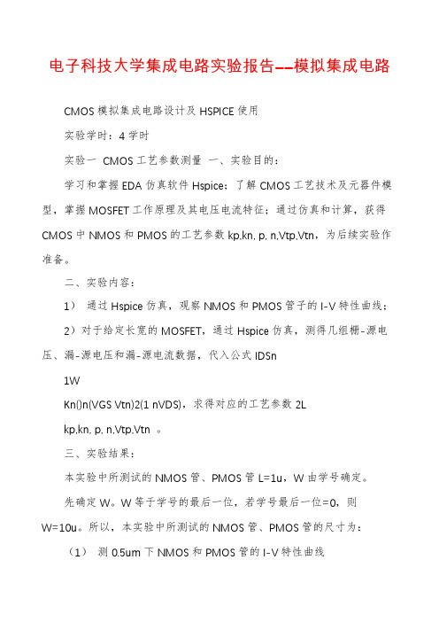
电子科技大学集成电路实验报告――模拟集成电路CMOS模拟集成电路设计及HSPICE使用实验学时:4学时实验一CMOS工艺参数测量一、实验目的:学习和掌握EDA仿真软件Hspice;了解CMOS工艺技术及元器件模型,掌握MOSFET工作原理及其电压电流特征;通过仿真和计算,获得CMOS中NMOS和PMOS的工艺参数kp,kn, p, n,Vtp,Vtn,为后续实验作准备。
二、实验内容:1)通过Hspice仿真,观察NMOS和PMOS管子的I-V特性曲线;2)对于给定长宽的MOSFET,通过Hspice仿真,测得几组栅-源电压、漏-源电压和漏-源电流数据,代入公式IDSn1WKn()n(VGS Vtn)2(1 nVDS),求得对应的工艺参数2Lkp,kn, p, n,Vtp,Vtn 。
三、实验结果:本实验中所测试的NMOS管、PMOS管L=1u,W由学号确定。
先确定W。
W等于学号的最后一位,若学号最后一位=0,则W=10u。
所以,本实验中所测试的NMOS管、PMOS管的尺寸为:(1)测0.5um下NMOS和PMOS管的I-V特性曲线所用工艺模型是TSMC 0.50um。
所测得的Vgs=1V时,NMOS管Vds从0V到2.5V变化时的I-V特性曲线为:所测得的Vds=1.2V时,NMOS管Vgs从0V到2.5V变化时的I-V特性曲线为:所测得的Vsg=1V时,PMOS管Vsd从0V到2.5V变化时的I-V特性曲线为:所测得的Vsd=1.2V时,PMOS管Vsg从0V到2.5V变化时的I-V特性曲线为:(2)计算TSMC 0.50um工艺库下mos管对应的工艺参数测试NMOS管相关参数,Hspice中仿真用源文件(.sp文件)为:NOMS I-V Characteristic M1 OUT IN 0 0 CMOSn L=1U W=8U VIN IN 0 1 VOUT OUT 0 1.2.***** LIST NODE POST *.DC VOUT 0 2.5 0.1 .DC VIN 0 2.5 0.1*.DC VOUT 0 2.5 0.1 VIN 0.8 1.0 0.2 .PRINT DC I(M1).LIB “C:\synopsys\project\tsmc_050um_model.lib"CMOS_MODELS .END所测得的NMOS管电流曲线为:所测的数据如下表:根据公式IDSn1Kn()n(VGS Vtn)2(1 nVDS),计算kn, n,Vtn,分别为:2Lkn 119 10-6, n 0.028,Vtn 1.37测试PMOS管相关参数,Hspice中仿真用源文件(.sp文件)为:POMS I-V CharacteristicM1 OUT IN Vdd Vdd CMOSP L=1U W=8UVIN Vdd IN 1 VOUT Vdd OUT 1.2.***** LIST NODE POST *.DC VOUT 0 2.5 0.1 .DC VIN 0 2.5 0.1*.DC VOUT 0 2.5 0.1 VIN 0.8 1.0 0.2.PRINT DC I(M2).LIB "C:\synopsys\project\tsmc_050um_model.lib"CMOS_MODELS .END所测得的PMOS管电流曲线为:所测的数据如下表:计算TSMC 0.50um 工艺中pmos 参数pptp,分别为:Kp 54.89 10-6, p 0.017,Vtp 0.927综上所述,可得:四、思考题2)不同工艺,p, n不同。

绪论0.1 选题背景当今的灯光艺术已经成为了一门走在时代前沿的时尚艺术。
灯具的种类也由以前构造简单、功能有限的白炽灯、荧光灯、聚光灯等,发展为今天的镜片反射式电脑灯、摇头式电脑灯、变色灯、电脑追光灯、激光灯等构造复杂、精密,功能丰富多样的现代灯具。
像我们经常在电视节目上看到的舞台灯光、城市景观灯、舞厅的各种闪光灯、街道上的霓虹灯等,其艺术性和表现力都产生了质的飞跃。
在基本光满足必要的照度和色调的基础上,根据场景气氛的需要,可以自由地组合出千姿百态、绚丽多彩、变幻无穷的灯光景观。
实现了艺术上的创新与突破,不断创造出令人惊叹、叫绝的视觉艺术效果,给人们带来了美的享受和心灵上的震撼。
就连我们最常见的楼道灯也一改过去那种人不开不亮,不关不灭的形象。
在我们生活的小区和工作的办公楼等地,每到晚上我们上下楼梯时,只要我们用手轻轻一摸开关上的按钮,灯就亮,人走后没一会灯又自动熄灭;或是天黑走过楼梯通道时,当有脚步声或其它声音时,楼道灯会自动点亮,提供照明,当人们进入房内或离开楼梯,楼道灯延时几分钟后会自动熄灭。
在白天,即使有声音。
楼道灯也不会亮。
之所以出现这种效果,这要归功于现代科学技术的发展,其中很重要的一点,就是现代电子技术的发展和创新。
它主要是利用一些电子元件,应用数字电子技术的逻辑器件设计电路进行控制。
像舞台上的灯光就是运用现代数字电子技术,按照场景的需要通过电脑程序进行控制;像楼道的灯就是通过安装一些电子开关进行控制。
社会在不断发展,技术也在不断的进步,电子技术在灯光照明控制中的应用也越来越广泛,越来越突出。
电子技术在电子技术在灯光照明控制中的应用已成为必须研究的课题。
在这里我主要从节能、便捷的角度,简单地介绍一下人们日常生活中经常见到的利用电子技术控制灯光的一些实际应用。
0.2 主要内容及研究意义目前电子技术在灯光控制中的应用已是越来越广泛。
电子技术在LED的通用照明和智能控制中的应用也是越来月明显,LED照明有许多独特的地方,其照明1不仅能实现亮度的调节,还能实现色彩与色温的调节。


Cmos集成电路研究任文娟(西北师范大学)摘要:集成电路的设计与测试是当代计算机技术研究的主要问题之一。
CMOS集成电路测试技术,受到人们的广泛关注。
本文介绍了CMOS集成电路测试技术基本原理和关键问题,探讨了电流测试的研究进展及现状,并提出了该技术的研究方向。
关键词:CMOS电路;电流测试;静态电流(I );动态电流(I ) DDQ DDT1 cmos集成电路的发展绝大多数集成电路是用硅的半导体材料制作的,因此也称为硅集成电路,另有少量的集成电路是用半导体材料砷化镓制造的。
集成电路可以按照不同的标准进行分类。
如果根据功能分类,有数字集成电路和模拟集成电路之分;以组成集成电路的器件来划分,可分为双极型和cmos两大类。
cmos集成电路因为具有功耗低、输入阻抗高、噪声容限高、电源电压范围宽、输出电压幅度与电源电压接近、对称的传输延迟和跃迁时间等优点,所以发展极为迅速。
1963年,国际固体电路会议首先发表了制成cmos集成电路的报告。
l 967年,RcA (美国无线电公司)开始试销cmos产品;20世纪70年代初正式推出比较完整的cmos标准数字电路产品CD4000系列,随后美国MoT0ROLA(摩托罗拉)公司也发表了Mcl4500系列,两者合称为4000系列。
CMOS集成电路的问世开创了微功耗电于学的先河。
在20世纪70年代中期,4000A系列发展为4000B系列,工作电压范围从A系列的3一15v扩展为B系列的3—18v,而且B系列除少量器件为非缓冲输出外,大部分器件都是缓冲输出的,使它的参数和性能比A系列有较大的改进。
1976年,由JEDEC(联合电子器件工程委员会)制定了统一规范,使B系列的功能和管脚排列标淮化,成为全世界各cmos 集成电路制造厂家共同生产的标准系列。
随着个人计算机及电子数据处理设备的普及和推广,特别是袖珍机和便携式电子设备的使用,对高速、低功耗器件的需求越来越迫切,这就促使这些仪器、设备的电源电压下降到3.3土o.3v的标准。

CMOS集成电路基础知识CMOS是ComplementaryMetal-OxideSemiconductor一词的缩写。
在业余电子制作中我们经常会用到它,这里系统、详细的介绍一些CMOS 集成电路基础知识及使用注意事项。
CMOS集成电路的性能及特点功耗低CMOS集成电路采用场效应管,且都是互补结构,工作时两个串联的场效应管总是处于一个管导通,另一个管截止的状态,电路静态功耗理论上为零。
实际上,由于存在漏电流,CMOS电路尚有微量静态功耗。
单个门电路的功耗典型值仅为20mW,动态功耗(在1MHz工作频率时)也仅为几mW。
工作电压范围宽CMOS集成电路供电简单,供电电源体积小,基本上不需稳压。
国产CC4000系列的集成电路,可在3~18V电压下正常工作。
逻辑摆幅大CMOS集成电路的逻辑高电平“1”、逻辑低电平“0”分别接近于电源高电位VDD及电影低电位VSS。
当VDD=15V,VSS=0V时,输出逻辑摆幅近似15V。
因此,CMOS集成电路的电压电压利用系数在各类集成电路中指标是较高的。
抗干扰能力强CMOS集成电路的电压噪声容限的典型值为电源电压的45%,保证值为电源电压的30%。
随着电源电压的增加,噪声容限电压的绝对值将成比例增加。
对于VDD=15V的供电电压(当VSS=0V时),电路将有7V 左右的噪声容限。
输入阻抗高CMOS集成电路的输入端一般都是由保护二极管和串联电阻构成的保护网络,故比一般场效应管的输入电阻稍小,但在正常工作电压范围内,这些保护二极管均处于反向偏置状态,直流输入阻抗取决于这些二极管的泄露电流,通常情况下,等效输入阻抗高达103~1011Ω,因此CMOS集成电路几乎不消耗驱动电路的功率。
温度稳定性能好由于CMOS集成电路的功耗很低,内部发热量少,而且,CMOS电路线路结构和电气参数都具有对称性,在温度环境发生变化时,某些参数能起到自动补偿作用,因而CMOS集成电路的温度特性非常好。

Research and Design of 25 Gb/s CMOS Optical Receiver Front-end Integrated CircuitsThesis Submitted to Nanjing University of Posts andTelecommunications for the Degree ofMaster of EngineeringByXu ChangSupervisor: Prof. Changchun ZhangApril 2020南京邮电大学学位论文原创性声明本人声明所呈交的学位论文是我个人在导师指导下进行的研究工作及取得的研究成果。
尽我所知,除了文中特别加以标注和致谢的地方外,论文中不包含其他人已经发表或撰写过的研究成果,也不包含为获得南京邮电大学或其它教育机构的学位或证书而使用过的材料。
与我一同工作的同志对本研究所做的任何贡献均已在论文中作了明确的说明并表示了谢意。
本人学位论文及涉及相关资料若有不实,愿意承担一切相关的法律责任。
研究生学号:____________ 研究生签名:_____________ 日期:____________南京邮电大学学位论文使用授权声明本人承诺所呈交的学位论文不涉及任何国家秘密,本人及导师为本论文的涉密责任并列第一责任人。
本人授权南京邮电大学可以保留并向国家有关部门或机构送交论文的复印件和电子文档;允许论文被查阅和借阅;可以将学位论文的全部或部分内容编入有关数据库进行检索;可以采用影印、缩印或扫描等复制手段保存、汇编本学位论文。
本文电子文档的内容和纸质论文的内容相一致。
论文的公布(包括刊登)授权南京邮电大学研究生院办理。
非国家秘密类涉密学位论文在解密后适用本授权书。
研究生签名:____________ 导师签名:____________ 日期:_____________摘要随着现今网络通信的快速发展,人们对于通信的容量和质量提出了更高的要求。

摘要开关电源芯片作为电源管理芯片的一个主体部分,因为有着高的转化效率和低的功耗等特点,使得开关电源芯片在便携式设备中有广泛的应用,其芯片的电路集成化、高工作效率及低纹波输出一直是研究的重点。
而其中误差放大器模块是开关电源中一个非常重要部分,它通过将采样反馈电压与基准电压比较,输入到PWM(脉宽调制)模块来控制占空比,从而实现输出电压的稳定,所以误差放大器是芯片电压反馈环路的关键。
本课题正是对于一种基于BiCMOS工艺,应用于开关电源芯片中的误差放大器深入研究,提出一种能用于高性能的开关电源芯片中的误差放大器电路,在保证高的增益和合适的带宽的同时,还具备稳定性高、瞬态响应速度快、对噪声有较强的抑制的特性。
本文从开关电源的工作原理,发展及前景讲起,着重介绍了开关电源中误差放大器的设计思路,工作原理,性能要求。
并对提出的误差放大器电路的差分输入级,共源共栅增益级,交叉耦合负载电路和输出级等设计思路进行了详细的分析。
最后,通过Hspice软件,在各种情况下,对误差放大器进行特性仿真验证。
关键词:DC-DC转换器误差放大器交叉耦合 CMRR PSRRAbstractAs a main part of power management chips, switching power chips have been widely applied to portable electronic fields for their features of high efficiency and low dissipation, and people have always been interested in some characteristics of switching power chips such as circuit integration, high efficiency and low output ripple voltage. Error amplifier is a crucial part in switching power chips; by comparing the sampled feedback voltage with a reference voltage, it generates an error voltage at PWM (Pulse wide Modulation) part to regulate the duty circle, thus realizing the stability of output voltage, so, error amplifier plays a key role in the voltage feedback loop. This paper designed and analyzed an error amplifier based on BiCMOS technology, which can be applied to switching power chips. The error amplifier has excellent performance: it not only fully meets the requirement of high gain and suitable bandwidth, also features with optimum stability, fast transient response and good resistance to noise.This paper begins with the principle, development and foresight of switching power supply, then it gives a particular description of error amplifier from its design guidelines, operation principles and performance requirements, further, it analyzed the differential input stage, common source-common gate gain stage, cross-coupled load circuit and output stage in detail. At last, the performance of the error amplifier is simulated by Hspice EDA software in all conditions and the simulation results are presented.Key Words:DC-DC Converter error amplifier cross-coupled CMRR PSRR目录摘要 (I)Abstract .......................................................... I I 1 选题背景 (1)1.1 本课题来源和意义 (1)1.2 开关电源控制技术 (1)1.3 开关电源的发展现状 (4)1.4 开关电源的前景和发展方向 (7)1.5 本论文章节安排以及主要内容 (8)2 误差放大器 (9)2.1 误差放大器工作原理 (9)2.2 误差放大器主要参数 (9)2.3. 本课题误差放大器性能要求 (11)2.4 本课题误差放大器性能指标小结 (13)3 误差放大器设计思路 (14)3.1 从工艺选择的角度 (14)3.2 工艺选择小结 (17)3.3 从电路选择的角度 (18)4 一种应用于电源管理芯片的误差放大器的设计与分析 (37)4.1 应用于电源管理芯片的误差放大器原理图 (37)4.2 实际仿真线路图 (38)5 总结 (59)致谢 (60)参考文献 (61)附录一直流仿真网表 (63)附录二交流分析增益仿真网表 (65)附录三 CMRR仿真网表 (67)附录四 PSRR仿真网表 (69)附录五延迟时间仿真网表 (71)附录六转换速率(Slew Rate)仿真网表 (73)1 选题背景1.1本课题来源和意义当今的电源管理芯片可从各种输入电源获得工作电压,范围包括从锂离子电池、碱性电池、镍电池到USB。
掛恅蚕襞砑覂翻2010僚瓬
pdf恅紫褫夔婓WAP傷銡擬极桄祥槽﹝膘祜蠟蚥珂恁寁TXTㄛ麼狟婥埭恅璃善掛儂脤艘﹝
Z迵﹛
?? ??? ??? ??? ??? ?? ??? ? ?? ﹛
?? ? ??輊傖萇繚撿衄腴髡瘧﹜ ? 雄脹蚥萸舒萇繚褫﹛蚚ㄢ?
聽諶宒萇喀麼啜ㄢ‵ㄧ?萇峆鼎萇ㄛ掘衄詢ㄛ腴髡瘧﹛凝諷秶羲壽﹛婓妏蚚聽諶宒萇喀奀ㄝ腴髡瘧馱釬夔悵涽萇坻衄誕﹛忭韜ㄛ詢
髡瘧馱釬奀﹛夔怀堤逋劂腔 雄萇霜﹝﹛袘萇繚 ? 峓啋璃屾ㄛ妏
蚚源晞ㄛ褫眕? 挭蚚衾嫘豢ㄛ敃怢﹛ㄛ ? 湍离ㄛ倠豪睿弅囀蚾庉脹源賒﹛
?? ???? 萇繚萇統杅 桶 ?垀尨﹛撓坋撿极睫瘍萇繚腔﹛妗暱茼蚚
婓狟醱賡庄﹝﹛
萇繚腔髡夔摯 茼蚚﹛
K ?? ㄣ﹛ ? ?ㄡ ?粒蚚邧蹈眻脣宒ㄡ鉠猾蚾ㄛ旋褐﹛ ?ㄡ ? ? ㄣㄣ 齬蹈 芞ㄡ垀尨ㄛ跪奪褐腔髡夔 桶ㄡ垀尨﹝ ?? ? ? ﹜ㄡㄛ﹛岆
豪﹛
欴諷秶傷ㄛ? 岆竘赻炵苀囀窒腔珨庌諫疏傷ㄝ絞 ? ﹛ ? 峈﹛ㄣ跺 ? ﹛萇繚埻燴摯 統杅﹛
最諷匢嫖? ? ? ??? 摩傖萇繚腔埻燴嘐 芞 ? 尨﹝垀﹛
萇繚腔馱釬徹最 狟ㄩ ??遠倛淥高莉汜奀笘闕喳ㄝ冪蜈﹛
萇繚莉汜 煦 ﹛
?§奀ㄝ ?? ﹜?ㄡ蠲﹜ ? ﹜ㄣ袨怓摯 怀堤豪欴 桶ㄢ垀蹈﹛ 笢?
﹛ ?? ?? 髡瘧﹜揖類羲壽諷秶傷ㄝ?﹝﹛岆珨 ? 奀峈詢﹛﹛髡瘧ㄛ ? ?祥 釬蚚ㄝ ??ˊㄟㄝ ?? 釬蚚ㄝ﹛※ㄟ§﹛ ?ㄗ﹛髡瘧ㄛ ?? ※?§峈
腴髡瘧﹝ˊ﹛
桶﹛ㄡ﹛
陓瘍﹛ 凝 陓瘍﹛迵俋諉腔擘坋豪﹛諷秶傷 ?? ? ﹜ㄢ﹛ㄡ?
﹛莉汜豪欴諷秶陓﹛瘍ㄛ豪欴諷秶陓瘍﹛冪祒鎢綴蔚 ? ?? 笢湔揣腔軗笱豪欴等啋囀 黍堤ㄛ堤腔陓瘍﹛黍冪 雄萇繚怀堤﹛ㄟㄡ 雄儕堤﹛ㄝ
桶﹛
唗瘍﹛
奪褐靡備狪髡夔﹛
諾﹛
唗瘍﹛
ㄠ﹛ㄢ
奪褐靡備摯髡夔﹛
? ?? 揖類羲 揖類傷﹛
ㄡ﹛ㄢ﹛
諾﹛ㄟㄢ 雄 ? ㄝ袓堤﹛
ㄠ﹛ ?? ㄣㄛ豪欴諷秶傷﹛ ?﹛ ? ㄛ豪欴諷訇傷﹛ㄤㄡ
? ㄝ豪欴諷秶傷﹛ㄢ
?ㄠㄝ 雄怀堤﹛ㄥ﹛ ?﹝勤 ?? ??諷秶﹛ㄛ狪 ?#ㄛ諉淥絕萇 ﹛ ?#ㄝ諉淥絕萇 ﹛ㄨ﹛
ㄠ﹛ㄟ
ㄢ﹛ ? ㄛ豪欴諷秶傷﹛ㄦㄣ ?﹛ㄟㄣㄧㄝ 雄儕堤﹛ㄠ﹛ㄟㄤ 雄怀堤﹛ㄨㄡ﹛ㄟㄥㄟㄝ 雄怀堤﹛ㄡ﹛ㄠ
ㄡ﹛ㄡ
炟﹛
統杅靡 ﹛ㄩ
?瘍敁﹛
渮
彸
沭
璃﹛
萎倰硉 ? 弇﹛等
萇弇 ?﹛埭萇﹛薧
噙怓萇 ? 鍌﹛
噙祩萇勯﹛
ㄤ﹛? ﹛? ﹛
?ㄠㄠ﹛﹛﹛﹛ ??
?ㄡ ? ? ﹛﹛﹛ㄟㄠ﹛※﹛ ?
ㄠㄛ﹛ˊ? ?﹛? ㄢㄛ怀堤羲繚﹛
? ? ﹛ˊ? ? ﹛?? ﹛ ?ㄝ怀堤羲繚﹛ ? ﹛ㄢ‵ㄤ﹛ ?
? ﹛ㄡ? 儕?萇霜﹛ㄝㄠ﹛ㄢ ? ? ﹛
喊雄萇霜﹛
?﹛詢腴髡瘧諷秶傷﹛ㄛ
?﹛ㄗ俋諉ㄘ祥﹛
ㄟㄦ 雄怀堤﹛ㄝ
? ㄝ華﹛﹛
??﹛ ?﹛ ? ? ㄢㄝ﹛ˊ ? ?#ˊㄠㄨㄝ ?﹛
ㄡㄡ ? ?﹛ㄝ﹛
雄萇霜﹛ 雄萇傑﹛
? ? ﹛ˊㄤ ? ? ﹛? ? ? ?ㄝ﹛ ? ? ?? ˊㄤ ? ﹛﹛﹛ㄠ ?ㄛ﹛ ?
ˊㄠㄨ﹛ㄝ? ˊㄢ﹛ ?
? ㄠ﹛
?? ﹛
ㄠㄠ﹛
?﹛ㄡ
? 揖類羲壽萇 ﹛ㄛ
?ㄜㄜ萇抾﹛§ㄝ
ㄡ﹛ㄢ
ㄡ﹛ㄣ
諾﹛
諾﹛
ㄥㄟ ? ? ㄝ﹛﹛
婓腴髡瘧馱釬奀ㄝ奀﹛唗闕喳莉汜珨跺腴髡瘧諷﹛秶闕喳陓瘍ㄛ ?? 怀堤陓﹛ ? 瘍冪腴髡瘧嶺秶闕喳陓瘍﹛
覃秶綴ㄝ倛傖珨坋晜闕喳﹛
陓瘍ㄝ闕遵峈埻懂 ? ??﹛怀堤陓瘍腔匐煦眳ㄝ涴﹛坋晜闕喳陓瘍 諷秶 雄﹛
萇喬ㄝ怀堤腔 歙髡瘧湮﹛
湮蔥腴﹛峈妏蚚源晞ㄛ萇繚笢﹛
扢离賸等傷揖類羲壽ㄝ藩﹛
揖類珨窊ㄝ揖類怀堤陓﹛
※ㄟ§﹜※ㄠ萇 採蛌﹛﹛馴ㄛ衄岍類怀堤 ?﹛ㄟ§硐峈﹛
萇 奀ㄛ符衄匢嫖怀﹛ㄝ﹛
婬陸萇鷇壽敕﹝﹛
ㄠㄗㄠ?﹛ㄣ軞 ?ㄘ
萇
赽
岍
賜﹛
ㄞ﹛
? ? ? 奻ㄜ ? ? ? ? ? ? ? ? ? ? ? ? ? ? ? ? ?﹛ㄟ
迵﹛
?? ㄣ ?ㄡ ?偽巠﹛ ? 隅腔部垀ㄝ瞰 ? 諫齪﹜梯泆﹜緛怢票﹛﹛瘧﹛ ?? ㄥ腔茼蚚 ? 統蕉?? ㄡ ? 蚚妗瞰﹛ ?ㄠ? ◆ ? ?茼
脹﹛※眕俋諉ㄜ諷寡﹜眻諉妏蚚蝠霜﹛ㄟ ? ? ㄦ ?萇埭ㄝ芞ㄢ峈
﹛茼﹛迼萇繚ˊ ? ?ㄡ ?珩夔眻諉﹛ 楷嫖 ? 奪ㄝ ? ? ? 忨▽萇繚 ﹛ㄣ垀﹛
? ﹛﹛﹝
敶﹛ㄢ﹛
ㄠ﹛ㄥ
? ﹛
唗瘍﹛ ?? ? ﹛ ? ﹛ㄧ﹛﹛ㄡㄢㄣ
萇﹛
繚﹛
髡﹛
夔﹛
ㄘ﹛
? ㄠ
? ?﹛ ?ㄥ ??
? ﹛ ?﹛ㄧ
囹萸匢嫖﹛
路匢嫖﹛
桶珨﹛ㄤ
﹝? ﹛
等萸衵唅匢嫖﹛
等萸﹛唅ㄠ嫖﹛﹛皛臻謠肮奀鏢﹛
唗瘍﹛ ? ﹛ ?ㄡ ? ﹛
萇﹛
繚﹛
髡﹛
夔﹛
▽﹛ㄡ﹛ㄢ﹛
? ﹛ ? ﹛﹛ ?
? ﹛
?? ㄢ ?ㄡ ?腔 ?‵ㄡ笱髡夔赻髡蛌遙﹛ ?? ㄣ ?ㄡ ?腔ㄢ‵ㄣ笱髡夔﹛雄蛌遙﹛ ?? ㄣ ?ㄡ ?腔ㄤ‵ㄥ笱髡夔彊髡蛌遙﹛
?? ㄣ ?ㄡ ?腔 ?‵ㄥ笱髡夔赻雄蛌遙﹛
?奀謠﹛甡馴鏢﹛ ? ? ?
ㄛ﹛
﹞﹛
?‵ㄥ笱豪欴赻雄蛌諉﹛ ?‵ㄥ笱豪欴赻雄蛌淂﹛
ㄧ﹛ ? ﹛▽﹛ ? ? ㄟ ?﹛插﹛﹛ㄣㄠ ? ﹛ ?ㄢ﹛ㄣ﹛
?‵ㄡ笱髡夔赻雄蛌遙﹛ㄢ‵ㄣ笱髡夔赻雄蛌遙﹛
? ?? ? ﹛ ?? ㄡ粒蚚 猾蚾ㄝ妏蚚ㄢ ? ㄡ? ?? ? ?聽諶萇喀ㄝ摩﹛ 萇繚睿俋峓萇繚郪蚾婓﹛? ‵ㄡ ? ?腔荂芃啣囀﹞ ? 覛豪﹜ ? ㄟ﹛酕﹛忑庉脹蚾庉 ㄝ 荂芃啣萇繚僗 芞ㄥ垀﹛ㄛ﹛
“﹛
?﹛ˋ
? ﹛ ?﹛?﹛﹛ㄟㄣㄢ
? ?﹛ ? ﹛﹛ㄣㄢ
ㄤ‵ㄥ髡夔赻笱雄蛌遙﹛
▽‵ㄥ笱髡夔赻雄蛌遙﹛
ㄨㄨㄠ爛﹛ ﹛﹛
1。