MAX244EQH-TD中文资料
- 格式:pdf
- 大小:368.45 KB
- 文档页数:36

General DescriptionThe MAX220–MAX249 family of line drivers/receivers is intended for all EIA/TIA-232E and V.28/V.24 communica-tions interfaces, particularly applications where ±12V is not available.These parts are especially useful in battery-powered sys-tems, since their low-power shutdown mode reduces power dissipation to less than 5µW. The MAX225,MAX233, MAX235, and MAX245/MAX246/MAX247 use no external components and are recommended for appli-cations where printed circuit board space is critical.________________________ApplicationsPortable Computers Low-Power Modems Interface TranslationBattery-Powered RS-232 Systems Multidrop RS-232 NetworksNext-Generation Device Features♦For Low-Voltage, Integrated ESD ApplicationsMAX3222E/MAX3232E/MAX3237E/MAX3241E/MAX3246E: +3.0V to +5.5V, Low-Power, Up to 1Mbps, True RS-232 Transceivers Using Four 0.1µF External Capacitors (MAX3246E Available in a UCSP™Package)♦For Low-Cost ApplicationsMAX221E: ±15kV ESD-Protected, +5V, 1µA,Single RS-232 Transceiver with AutoShutdown™MAX220–MAX249+5V-Powered, Multichannel RS-232Drivers/Receivers________________________________________________________________Maxim Integrated Products 1Selection Table19-4323; Rev 15; 1/06Power No. of NominalSHDN RxPart Supply RS-232No. of Cap. Value & Three-Active in Data Rate Number (V)Drivers/Rx Ext. Caps (µF)State SHDN (kbps)FeaturesMAX220+52/240.047/0.33No —120Ultra-low-power, industry-standard pinout MAX222+52/2 4 0.1Yes —200Low-power shutdownMAX223 (MAX213)+54/54 1.0 (0.1)Yes ✔120MAX241 and receivers active in shutdown MAX225+55/50—Yes ✔120Available in SOMAX230 (MAX200)+55/04 1.0 (0.1)Yes —120 5 drivers with shutdownMAX231 (MAX201)+5 and2/2 2 1.0 (0.1)No —120Standard +5/+12V or battery supplies; +7.5 to +13.2same functions as MAX232MAX232 (MAX202)+52/24 1.0 (0.1)No —120 (64)Industry standardMAX232A+52/240.1No —200Higher slew rate, small caps MAX233 (MAX203)+52/20— No —120No external capsMAX233A+52/20—No —200No external caps, high slew rate MAX234 (MAX204)+54/04 1.0 (0.1)No —120Replaces 1488MAX235 (MAX205)+55/50—Yes —120No external capsMAX236 (MAX206)+54/34 1.0 (0.1)Yes —120Shutdown, three stateMAX237 (MAX207)+55/34 1.0 (0.1)No —120Complements IBM PC serial port MAX238 (MAX208)+54/44 1.0 (0.1)No —120Replaces 1488 and 1489MAX239 (MAX209)+5 and3/52 1.0 (0.1)No —120Standard +5/+12V or battery supplies;+7.5 to +13.2single-package solution for IBM PC serial port MAX240+55/54 1.0Yes —120DIP or flatpack package MAX241 (MAX211)+54/54 1.0 (0.1)Yes —120Complete IBM PC serial port MAX242+52/240.1Yes ✔200Separate shutdown and enableMAX243+52/240.1No —200Open-line detection simplifies cabling MAX244+58/104 1.0No —120High slew rateMAX245+58/100—Yes ✔120High slew rate, int. caps, two shutdown modes MAX246+58/100—Yes ✔120High slew rate, int. caps, three shutdown modes MAX247+58/90—Yes ✔120High slew rate, int. caps, nine operating modes MAX248+58/84 1.0Yes ✔120High slew rate, selective half-chip enables MAX249+56/1041.0Yes✔120Available in quad flatpack packageFor pricing, delivery, and ordering information,please contact Maxim/Dallas Direct!at 1-888-629-4642, or visit Maxim’s website at .Ordering InformationOrdering Information continued at end of data sheet.*Contact factory for dice specifications.AutoShutdown and UCSP are trademarks of Maxim Integrated Products, Inc.M A X 220–M A X 249+5V-Powered, Multichannel RS-232Drivers/Receivers 2_______________________________________________________________________________________ABSOLUTE MAXIMUM RATINGS—MAX220/222/232A/233A/242/243ELECTRICAL CHARACTERISTICS—MAX220/222/232A/233A/242/243Note 1:For the MAX220, V+ and V- can have a maximum magnitude of 7V, but their absolute difference cannot exceed 13V.Note 2:Input voltage measured with T OUT in high-impedance state, SHDN or V CC = 0V.Note 3:Maximum reflow temperature for the MAX233A is +225°C.Stresses beyond those listed under “Absolute Maximum Ratings” may cause permanent damage to the device. These are stress ratings only, and functional operation of the device at these or any other conditions beyond those indicated in the operational sections of the specifications is not implied. Exposure to absolute maximum rating conditions for extended periods may affect device reliability.Supply Voltage (V CC )...............................................-0.3V to +6V V+ (Note 1)..................................................(V CC - 0.3V) to +14V V- (Note 1).............................................................+0.3V to +14V Input VoltagesT IN ..............................................................-0.3V to (V CC - 0.3V)R IN (Except MAX220)........................................................±30V R IN (MAX220).....................................................................±25V T OUT (Except MAX220) (Note 2).......................................±15V T OUT (MAX220)...............................................................±13.2V Output VoltagesT OUT ...................................................................................±15V R OUT .........................................................-0.3V to (V CC + 0.3V)Driver/Receiver Output Short Circuited to GND.........Continuous Continuous Power Dissipation (T A = +70°C)16-Pin Plastic DIP (derate 10.53mW/°C above +70°C)..842mW18-Pin Plastic DIP (derate 11.11mW/°C above +70°C)..889mW 20-Pin Plastic DIP (derate 8.00mW/°C above +70°C)..440mW 16-Pin Narrow SO (derate 8.70mW/°C above +70°C)...696mW 16-Pin Wide SO (derate 9.52mW/°C above +70°C)......762mW 18-Pin Wide SO (derate 9.52mW/°C above +70°C)......762mW 20-Pin Wide SO (derate 10.00mW/°C above +70°C)....800mW 20-Pin SSOP (derate 8.00mW/°C above +70°C)..........640mW 16-Pin CERDIP (derate 10.00mW/°C above +70°C).....800mW 18-Pin CERDIP (derate 10.53mW/°C above +70°C).....842mW Operating Temperature RangesMAX2_ _AC_ _, MAX2_ _C_ _.............................0°C to +70°C MAX2_ _AE_ _, MAX2_ _E_ _..........................-40°C to +85°C MAX2_ _AM_ _, MAX2_ _M_ _.......................-55°C to +125°C Storage Temperature Range.............................-65°C to +160°C Lead Temperature (soldering, 10s) (Note 3)...................+300°CMAX220–MAX249+5V-Powered, Multichannel RS-232Drivers/Receivers_______________________________________________________________________________________3Note 4:MAX243 R2OUT IN ELECTRICAL CHARACTERISTICS—MAX220/222/232A/233A/242/243 (continued)M A X 220–M A X 249+5V-Powered, Multichannel RS-232Drivers/Receivers 4_________________________________________________________________________________________________________________________________Typical Operating CharacteristicsMAX220/MAX222/MAX232A/MAX233A/MAX242/MAX243108-1051525OUTPUT VOLTAGE vs. LOAD CURRENT-4-6-8-2642LOAD CURRENT (mA)O U T P U T V O L T A G E (V )1002011104104060AVAILABLE OUTPUT CURRENTvs. DATA RATE65798DATA RATE (kb/s)O U T P U T C U R R E N T (m A )203050+10V-10VMAX222/MAX242ON-TIME EXITING SHUTDOWN+5V +5V 0V0V 500μs/div V +, V - V O L T A G E (V )ELECTRICAL CHARACTERISTICS—MAX220/222/232A/233A/242/243 (continued)(V CC = +5V ±10%, C1–C4 = 0.1µF‚ MAX220, C1 = 0.047µF, C2–C4 = 0.33µF, T A = T MIN to T MAX ‚ unless otherwise noted.)MAX220–MAX249+5V-Powered, Multichannel RS-232Drivers/Receivers_______________________________________________________________________________________5V CC ...........................................................................-0.3V to +6V V+................................................................(V CC - 0.3V) to +14V V-............................................................................+0.3V to -14V Input VoltagesT IN ............................................................-0.3V to (V CC + 0.3V)R IN ......................................................................................±30V Output VoltagesT OUT ...................................................(V+ + 0.3V) to (V- - 0.3V)R OUT .........................................................-0.3V to (V CC + 0.3V)Short-Circuit Duration, T OUT ......................................Continuous Continuous Power Dissipation (T A = +70°C)14-Pin Plastic DIP (derate 10.00mW/°C above +70°C)....800mW 16-Pin Plastic DIP (derate 10.53mW/°C above +70°C)....842mW 20-Pin Plastic DIP (derate 11.11mW/°C above +70°C)....889mW 24-Pin Narrow Plastic DIP(derate 13.33mW/°C above +70°C)..........1.07W24-Pin Plastic DIP (derate 9.09mW/°C above +70°C)......500mW 16-Pin Wide SO (derate 9.52mW/°C above +70°C).........762mW20-Pin Wide SO (derate 10.00mW/°C above +70°C).......800mW 24-Pin Wide SO (derate 11.76mW/°C above +70°C).......941mW 28-Pin Wide SO (derate 12.50mW/°C above +70°C) .............1W 44-Pin Plastic FP (derate 11.11mW/°C above +70°C).....889mW 14-Pin CERDIP (derate 9.09mW/°C above +70°C)..........727mW 16-Pin CERDIP (derate 10.00mW/°C above +70°C)........800mW 20-Pin CERDIP (derate 11.11mW/°C above +70°C)........889mW 24-Pin Narrow CERDIP(derate 12.50mW/°C above +70°C)..............1W24-Pin Sidebraze (derate 20.0mW/°C above +70°C)..........1.6W 28-Pin SSOP (derate 9.52mW/°C above +70°C).............762mW Operating Temperature RangesMAX2 _ _ C _ _......................................................0°C to +70°C MAX2 _ _ E _ _...................................................-40°C to +85°C MAX2 _ _ M _ _......................................................-55°C to +125°C Storage Temperature Range.............................-65°C to +160°C Lead Temperature (soldering, 10s) (Note 4)...................+300°CABSOLUTE MAXIMUM RATINGS—MAX223/MAX230–MAX241ELECTRICAL CHARACTERISTICS—MAX223/MAX230–MAX241(MAX223/230/232/234/236/237/238/240/241, V CC = +5V ±10; MAX233/MAX235, V CC = 5V ±5%‚ C1–C4 = 1.0µF; MAX231/MAX239,V CC = 5V ±10%; V+ = 7.5V to 13.2V; T A = T MIN to T MAX ; unless otherwise noted.)Stresses beyond those listed under “Absolute Maximum Ratings” may cause permanent damage to the device. These are stress ratings only, and functional operation of the device at these or any other conditions beyond those indicated in the operational sections of the specifications is not implied. Exposure to absolute maximum rating conditions for extended periods may affect device reliability.Note 4:Maximum reflow temperature for the MAX233/MAX235 is +225°C.M A X 220–M A X 249+5V-Powered, Multichannel RS-232Drivers/Receivers 6_______________________________________________________________________________________ELECTRICAL CHARACTERISTICS—MAX223/MAX230–MAX241 (continued)(MAX223/230/232/234/236/237/238/240/241, V CC = +5V ±10; MAX233/MAX235, V CC = 5V ±5%‚ C1–C4 = 1.0µF; MAX231/MAX239,V CC = 5V ±10%; V+ = 7.5V to 13.2V; T A = T MIN to T MAX ; unless otherwise noted.)MAX220–MAX249+5V-Powered, Multichannel RS-232Drivers/Receivers_______________________________________________________________________________________78.56.54.55.5TRANSMITTER OUTPUT VOLTAGE (V OH ) vs. V CC7.08.0V CC (V)V O H (V )5.07.57.46.02500TRANSMITTER OUTPUT VOLTAGE (V OH )vs. LOAD CAPACITANCE AT DIFFERENT DATA RATES6.46.27.27.0LOAD CAPACITANCE (pF)V O H (V )1500100050020006.86.612.04.02500TRANSMITTER SLEW RATE vs. LOAD CAPACITANCE6.05.011.09.010.0LOAD CAPACITANCE (pF)S L E W R A T E (V /μs )1500100050020008.07.0-6.0-9.04.55.5TRANSMITTER OUTPUT VOLTAGE (V OL ) vs. V CC-8.0-8.5-6.5-7.0V CC (V)V O L (V )5.0-7.5-6.0-7.62500TRANSMITTER OUTPUT VOLTAGE (V OL )vs. LOAD CAPACITANCE AT DIFFERENT DATA RATES-7.0-7.2-7.4-6.2-6.4LOAD CAPACITANCE (pF)V O L (V )150010005002000-6.6-6.810-105101520253035404550TRANSMITTER OUTPUT VOLTAGE (V+, V-)vs. LOAD CURRENT-2-6-4-886CURRENT (mA)V +, V - (V )420__________________________________________Typical Operating CharacteristicsMAX223/MAX230–MAX241*SHUTDOWN POLARITY IS REVERSED FOR NON MAX241 PARTSV+, V- WHEN EXITING SHUTDOWN(1μF CAPACITORS)MAX220-13SHDN*V-O V+500ms/divM A X 220–M A X 249+5V-Powered, Multichannel RS-232Drivers/Receivers 8_______________________________________________________________________________________ABSOLUTE MAXIMUM RATINGS—MAX225/MAX244–MAX249ELECTRICAL CHARACTERISTICS—MAX225/MAX244–MAX249(MAX225, V CC = 5.0V ±5%; MAX244–MAX249, V CC = +5.0V ±10%, external capacitors C1–C4 = 1µF; T A = T MIN to T MAX ; unless oth-erwise noted.)Stresses beyond those listed under “Absolute Maximum Ratings” may cause permanent damage to the device. These are stress ratings only, and functional operation of the device at these or any other conditions beyond those indicated in the operational sections of the specifications is not implied. Exposure to absolute maximum rating conditions for extended periods may affect device reliability.Supply Voltage (V CC )...............................................-0.3V to +6V Input VoltagesT IN ‚ ENA , ENB , ENR , ENT , ENRA ,ENRB , ENTA , ENTB ..................................-0.3V to (V CC + 0.3V)R IN .....................................................................................±25V T OUT (Note 5).....................................................................±15V R OUT ........................................................-0.3V to (V CC + 0.3V)Short Circuit (one output at a time)T OUT to GND............................................................Continuous R OUT to GND............................................................ContinuousContinuous Power Dissipation (T A = +70°C)28-Pin Wide SO (derate 12.50mW/°C above +70°C).............1W 40-Pin Plastic DIP (derate 11.11mW/°C above +70°C)...611mW 44-Pin PLCC (derate 13.33mW/°C above +70°C)...........1.07W Operating Temperature RangesMAX225C_ _, MAX24_C_ _ ..................................0°C to +70°C MAX225E_ _, MAX24_E_ _ ...............................-40°C to +85°C Storage Temperature Range.............................-65°C to +160°C Lead Temperature (soldering,10s) (Note 6)....................+300°CNote 5:Input voltage measured with transmitter output in a high-impedance state, shutdown, or V CC = 0V.Note 6:Maximum reflow temperature for the MAX225/MAX245/MAX246/MAX247 is +225°C.MAX220–MAX249+5V-Powered, Multichannel RS-232Drivers/Receivers_______________________________________________________________________________________9Note 7:The 300Ωminimum specification complies with EIA/TIA-232E, but the actual resistance when in shutdown mode or V CC =0V is 10M Ωas is implied by the leakage specification.ELECTRICAL CHARACTERISTICS—MAX225/MAX244–MAX249 (continued)(MAX225, V CC = 5.0V ±5%; MAX244–MAX249, V CC = +5.0V ±10%, external capacitors C1–C4 = 1µF; T A = T MIN to T MAX ; unless oth-erwise noted.)M A X 220–M A X 249+5V-Powered, Multichannel RS-232Drivers/Receivers 10________________________________________________________________________________________________________________________________Typical Operating CharacteristicsMAX225/MAX244–MAX24918212345TRANSMITTER SLEW RATE vs. LOAD CAPACITANCE86416LOAD CAPACITANCE (nF)T R A N S M I T T E R S L E W R A T E (V /μs )14121010-105101520253035OUTPUT VOLTAGEvs. LOAD CURRENT FOR V+ AND V--2-4-6-88LOAD CURRENT (mA)O U T P U T V O L T A G E (V )64209.05.012345TRANSMITTER OUTPUT VOLTAGE (V+, V-)vs. LOAD CAPACITANCE AT DIFFERENT DATA RATES6.05.58.5LOAD CAPACITANCE (nF)V +, V (V )8.07.57.06.5MAX220–MAX249Drivers/ReceiversFigure 1. Transmitter Propagation-Delay Timing Figure 2. Receiver Propagation-Delay TimingFigure 3. Receiver-Output Enable and Disable Timing Figure 4. Transmitter-Output Disable TimingM A X 220–M A X 249Drivers/Receivers ENT ENR OPERATION STATUS TRANSMITTERSRECEIVERS00Normal Operation All Active All Active 01Normal Operation All Active All 3-State10Shutdown All 3-State All Low-Power Receive Mode 11ShutdownAll 3-StateAll 3-StateTable 1a. MAX245 Control Pin ConfigurationsENT ENR OPERATION STATUS TRANSMITTERS RECEIVERSTA1–TA4TB1–TB4RA1–RA5RB1–RB500Normal Operation All Active All Active All Active All Active 01Normal Operation All Active All Active RA1–RA4 3-State,RA5 Active RB1–RB4 3-State,RB5 Active 1ShutdownAll 3-StateAll 3-StateAll Low-Power Receive Mode All Low-Power Receive Mode 11Shutdown All 3-State All 3-StateRA1–RA4 3-State,RA5 Low-Power Receive ModeRB1–RB4 3-State,RB5 Low-Power Receive ModeTable 1b. MAX245 Control Pin ConfigurationsTable 1c. MAX246 Control Pin ConfigurationsENA ENB OPERATION STATUS TRANSMITTERS RECEIVERSTA1–TA4TB1–TB4RA1–RA5RB1–RB500Normal Operation All Active All Active All Active All Active 01Normal Operation All Active All 3-State All Active RB1–RB4 3-State,RB5 Active 1ShutdownAll 3-StateAll ActiveRA1–RA4 3-State,RA5 Active All Active 11Shutdown All 3-State All 3-StateRA1–RA4 3-State,RA5 Low-Power Receive ModeRB1–RB4 3-State,RA5 Low-Power Receive ModeMAX220–MAX249Drivers/ReceiversM A X 220–M A X 249_______________Detailed DescriptionThe MAX220–MAX249 contain four sections: dual charge-pump DC-DC voltage converters, RS-232 dri-vers, RS-232 receivers, and receiver and transmitter enable control inputs.Dual Charge-Pump Voltage ConverterThe MAX220–MAX249 have two internal charge-pumps that convert +5V to ±10V (unloaded) for RS-232 driver operation. The first converter uses capacitor C1 to dou-ble the +5V input to +10V on C3 at the V+ output. The second converter uses capacitor C2 to invert +10V to -10V on C4 at the V- output.A small amount of power may be drawn from the +10V (V+) and -10V (V-) outputs to power external circuitry (see the Typical Operating Characteristics section),except on the MAX225 and MAX245–MAX247, where these pins are not available. V+ and V- are not regulated,so the output voltage drops with increasing load current.Do not load V+ and V- to a point that violates the mini-mum ±5V EIA/TIA-232E driver output voltage when sourcing current from V+ and V- to external circuitry. When using the shutdown feature in the MAX222,MAX225, MAX230, MAX235, MAX236, MAX240,MAX241, and MAX245–MAX249, avoid using V+ and V-to power external circuitry. When these parts are shut down, V- falls to 0V, and V+ falls to +5V. For applica-tions where a +10V external supply is applied to the V+pin (instead of using the internal charge pump to gen-erate +10V), the C1 capacitor must not be installed and the SHDN pin must be tied to V CC . This is because V+is internally connected to V CC in shutdown mode.RS-232 DriversThe typical driver output voltage swing is ±8V when loaded with a nominal 5k ΩRS-232 receiver and V CC =+5V. Output swing is guaranteed to meet the EIA/TIA-232E and V.28 specification, which calls for ±5V mini-mum driver output levels under worst-case conditions.These include a minimum 3k Ωload, V CC = +4.5V, and maximum operating temperature. Unloaded driver out-put voltage ranges from (V+ -1.3V) to (V- +0.5V).Input thresholds are both TTL and CMOS compatible.The inputs of unused drivers can be left unconnected since 400k Ωinput pullup resistors to V CC are built in (except for the MAX220). The pullup resistors force the outputs of unused drivers low because all drivers invert.The internal input pullup resistors typically source 12µA,except in shutdown mode where the pullups are dis-abled. Driver outputs turn off and enter a high-imped-ance state—where leakage current is typically microamperes (maximum 25µA)—when in shutdownmode, in three-state mode, or when device power is removed. Outputs can be driven to ±15V. The power-supply current typically drops to 8µA in shutdown mode.The MAX220 does not have pullup resistors to force the outputs of the unused drivers low. Connect unused inputs to GND or V CC .The MAX239 has a receiver three-state control line, and the MAX223, MAX225, MAX235, MAX236, MAX240,and MAX241 have both a receiver three-state control line and a low-power shutdown control. Table 2 shows the effects of the shutdown control and receiver three-state control on the receiver outputs.The receiver TTL/CMOS outputs are in a high-imped-ance, three-state mode whenever the three-state enable line is high (for the MAX225/MAX235/MAX236/MAX239–MAX241), and are also high-impedance whenever the shutdown control line is high.When in low-power shutdown mode, the driver outputs are turned off and their leakage current is less than 1µA with the driver output pulled to ground. The driver output leakage remains less than 1µA, even if the transmitter output is backdriven between 0V and (V CC + 6V). Below -0.5V, the transmitter is diode clamped to ground with 1k Ωseries impedance. The transmitter is also zener clamped to approximately V CC + 6V, with a series impedance of 1k Ω.The driver output slew rate is limited to less than 30V/µs as required by the EIA/TIA-232E and V.28 specifica-tions. Typical slew rates are 24V/µs unloaded and 10V/µs loaded with 3Ωand 2500pF.RS-232 ReceiversEIA/TIA-232E and V.28 specifications define a voltage level greater than 3V as a logic 0, so all receivers invert.Input thresholds are set at 0.8V and 2.4V, so receivers respond to TTL level inputs as well as EIA/TIA-232E and V.28 levels.The receiver inputs withstand an input overvoltage up to ±25V and provide input terminating resistors withDrivers/ReceiversTable 2. Three-State Control of ReceiversMAX220–MAX249Drivers/Receiversnominal 5k Ωvalues. The receivers implement Type 1interpretation of the fault conditions of V.28 and EIA/TIA-232E.The receiver input hysteresis is typically 0.5V with a guaranteed minimum of 0.2V. This produces clear out-put transitions with slow-moving input signals, even with moderate amounts of noise and ringing. The receiver propagation delay is typically 600ns and is independent of input swing direction.Low-Power Receive ModeThe low-power receive mode feature of the MAX223,MAX242, and MAX245–MAX249 puts the IC into shut-down mode but still allows it to receive information. This is important for applications where systems are periodi-cally awakened to look for activity. Using low-power receive mode, the system can still receive a signal that will activate it on command and prepare it for communi-cation at faster data rates. This operation conserves system power.Negative Threshold—MAX243The MAX243 is pin compatible with the MAX232A, differ-ing only in that RS-232 cable fault protection is removed on one of the two receiver inputs. This means that control lines such as CTS and RTS can either be driven or left floating without interrupting communication. Different cables are not needed to interface with different pieces of equipment.The input threshold of the receiver without cable fault protection is -0.8V rather than +1.4V. Its output goes positive only if the input is connected to a control line that is actively driven negative. If not driven, it defaults to the 0 or “OK to send” state. Normally‚ the MAX243’s other receiver (+1.4V threshold) is used for the data line (TD or RD)‚ while the negative threshold receiver is con-nected to the control line (DTR‚ DTS‚ CTS‚ RTS, etc.). Other members of the RS-232 family implement the optional cable fault protection as specified by EIA/TIA-232E specifications. This means a receiver output goes high whenever its input is driven negative‚ left floating‚or shorted to ground. The high output tells the serial communications IC to stop sending data. To avoid this‚the control lines must either be driven or connected with jumpers to an appropriate positive voltage level.Shutdown—MAX222–MAX242On the MAX222‚ MAX235‚ MAX236‚ MAX240‚ and MAX241‚ all receivers are disabled during shutdown.On the MAX223 and MAX242‚ two receivers continue to operate in a reduced power mode when the chip is in shutdown. Under these conditions‚ the propagation delay increases to about 2.5µs for a high-to-low input transition. When in shutdown, the receiver acts as a CMOS inverter with no hysteresis. The MAX223 and MAX242 also have a receiver output enable input (EN for the MAX242 and EN for the MAX223) that allows receiver output control independent of SHDN (SHDN for MAX241). With all other devices‚ SHDN (SH DN for MAX241) also disables the receiver outputs.The MAX225 provides five transmitters and five receivers‚ while the MAX245 provides ten receivers and eight transmitters. Both devices have separate receiver and transmitter-enable controls. The charge pumps turn off and the devices shut down when a logic high is applied to the ENT input. In this state, the supply cur-rent drops to less than 25µA and the receivers continue to operate in a low-power receive mode. Driver outputs enter a high-impedance state (three-state mode). On the MAX225‚ all five receivers are controlled by the ENR input. On the MAX245‚ eight of the receiver out-puts are controlled by the ENR input‚ while the remain-ing two receivers (RA5 and RB5) are always active.RA1–RA4 and RB1–RB4 are put in a three-state mode when ENR is a logic high.Receiver and Transmitter EnableControl InputsThe MAX225 and MAX245–MAX249 feature transmitter and receiver enable controls.The receivers have three modes of operation: full-speed receive (normal active)‚ three-state (disabled)‚ and low-power receive (enabled receivers continue to function at lower data rates). The receiver enable inputs control the full-speed receive and three-state modes. The transmitters have two modes of operation: full-speed transmit (normal active) and three-state (disabled). The transmitter enable inputs also control the shutdown mode. The device enters shutdown mode when all transmitters are disabled. Enabled receivers function in the low-power receive mode when in shutdown.M A X 220–M A X 249Tables 1a–1d define the control states. The MAX244has no control pins and is not included in these tables. The MAX246 has ten receivers and eight drivers with two control pins, each controlling one side of the device. A logic high at the A-side control input (ENA )causes the four A-side receivers and drivers to go into a three-state mode. Similarly, the B-side control input (ENB ) causes the four B-side drivers and receivers to go into a three-state mode. As in the MAX245, one A-side and one B-side receiver (RA5 and RB5) remain active at all times. The entire device is put into shut-down mode when both the A and B sides are disabled (ENA = ENB = +5V).The MAX247 provides nine receivers and eight drivers with four control pins. The ENRA and ENRB receiver enable inputs each control four receiver outputs. The ENTA and ENTB transmitter enable inputs each control four drivers. The ninth receiver (RB5) is always active.The device enters shutdown mode with a logic high on both ENTA and ENTB .The MAX248 provides eight receivers and eight drivers with four control pins. The ENRA and ENRB receiver enable inputs each control four receiver outputs. The ENTA and ENTB transmitter enable inputs control four drivers each. This part does not have an always-active receiver. The device enters shutdown mode and trans-mitters go into a three-state mode with a logic high on both ENTA and ENTB .The MAX249 provides ten receivers and six drivers with four control pins. The ENRA and ENRB receiver enable inputs each control five receiver outputs. The ENTA and ENTB transmitter enable inputs control three dri-vers each. There is no always-active receiver. The device enters shutdown mode and transmitters go into a three-state mode with a logic high on both ENTA and ENTB . In shutdown mode, active receivers operate in a low-power receive mode at data rates up to 20kb/s.__________Applications InformationFigures 5 through 25 show pin configurations and typi-cal operating circuits. In applications that are sensitive to power-supply noise, V CC should be decoupled to ground with a capacitor of the same value as C1 and C2 connected as close as possible to the device.Drivers/Receivers。

MAXIM(美信)命名规则MAXIM前缀是“MAX”。
DALLAS则是以“DS”开头。
MAX×××或MAX××××说明:1后缀CSA、CWA 其中C表示普通级,S表示表贴,W表示宽体表贴。
2 后缀CWI表示宽体表贴,EEWI宽体工业级表贴,后缀MJA或883为军级。
3 CPA、BCPI、BCPP、CPP、CCPP、CPE、CPD、ACPA后缀均为普通双列直插。
举例MAX202CPE、CPE普通ECPE普通带抗静电保护MAX202EEPE 工业级抗静电保护(-45℃-85℃)说明 E指抗静电保护MAXIM数字排列分类1字头模拟器 2字头滤波器 3字头多路开关4字头放大器 5字头数模转换器 6字头电压基准7字头电压转换 8字头复位器 9字头比较器DALLAS命名规则例如DS1210N.S. DS1225Y-100INDN=工业级S=表贴宽体 MCG=DIP封Z=表贴宽体 MNG=DIP工业级IND=工业级 QCG=PLCC封 Q=QFP下面是MAXIM的命名规则:三字母后缀:例如:MAX358CPDC = 温度范围P = 封装类型D = 管脚数温度范围:C = 0℃ 至70℃ (商业级)I = -20℃ 至+85℃ (工业级)E = -40℃ 至+85℃ (扩展工业级)A = -40℃ 至+85℃ (航空级)M = -55℃ 至+125℃ (军品级)封装类型:A SSOP(缩小外型封装)B CERQUADC TO-220, TQFP(薄型四方扁平封装)D 陶瓷铜顶封装E 四分之一大的小外型封装F 陶瓷扁平封装H 模块封装, SBGA(超级球式栅格阵列, 5x5 TQFP) 四字母后缀:例如:MAX1480ACPIA = 指标等级或附带功能C = 温度范围P = 封装类型I = 管脚数温度范围:C = 0℃ 至70℃ (商业级)I = -20℃ 至+85℃ (工业级)E = -40℃ 至+85℃ (扩展工业级)A = -40℃ 至+85℃ (航空级)M = -55℃ 至+125℃ (军品级)封装类型:A SSOP(缩小外型封装)B CERQUADC TO-220, TQFP(薄型四方扁平封装)D 陶瓷铜顶封装E 四分之一大的小外型封装F 陶瓷扁平封装H 模块封装, SBGA(超级球式栅格阵列, 5x5 TQFP) J CERDIP (陶瓷双列直插)K TO-3 塑料接脚栅格阵列L LCC (无引线芯片承载封装)M MQFP (公制四方扁平封装)N 窄体塑封双列直插P 塑封双列直插Q PLCC (塑料式引线芯片承载封装)R 窄体陶瓷双列直插封装(300mil)S 小外型封装T TO5,TO-99,TO-100U TSSOP,μMAX,SOTW 宽体小外型封装(300mil)X SC-70(3脚,5脚,6脚)Y 窄体铜顶封装Z TO-92,MQUAD/D 裸片/PR 增强型塑封/W 晶圆管脚数:A: 8B: 10,64C: 12,192D: 14E: 16F: 22,256G: 24H: 44I: 28J: 32K: 5,68L: 40M: 7,48 N: 18O: 42 P: 20Q: 2,100 R: 3,84S: 4,80 T: 6,160U: 60 V: 8(圆形)W: 10(圆形) X: 36Y: 8(圆形) Z: 10(圆形)。

244LD型智能浮筒液位(界位)变送器辽制目录1. 概述.............................................................. - 0 -2. 产品特色............................................................ - 1 -3. 主要技术参数........................................................ - 2 -4. 变送器选型表........................................................ - 3 -5. 测量原理............................................................ - 4 -6. 安装与电气连接...................................................... - 5 -7. 运行调试............................................................ - 7 -8. 现场显示............................................................ - 8 -9. 维护、修理.......................................................... - 8 -10. 安全要求........................................................... - 9 -11. 变送器外形图及安装尺寸............................................ - 10 -12. 变送器的供电...................................................... - 11 -13. 订购仪表注意事项.................................................. - 13 -14. 包装、标志、运输及贮存............................................ - 13 -15. 计算公式及计算方法................................................ - 14 -16.故障分析与排除..................................................... - 15 -17. 变送器的调试...................................................... - 14 -1.概述244LD型智能浮筒液(界)位变送器在工况下可以实现持续的液体液位、界位及密度的测量。


1CAUTION: These devices are sensitive to electrostatic discharge; follow proper IC Handling Procedures.1-888-INTERSIL or 321-724-7143|Copyright © Intersil Corporation 1999March 1998ACS244MSRadiation Hardened Non-Inverting,Octal, Three-State Buffer/Line DriverFeatures•QML Qualified Per MIL-PRF-38535 Requirements • 1.25Micron Radiation Hardened SOS CMOS•Radiation Environment-Latch-up Free Under any Conditions-Total Dose. . . . . . . . . . . . . . . . . . . . . .3 x 105RAD(Si)-SEU Immunity. . . . . . . . . . .<1 x 10⁻¹⁰ Errors/Bit/Day -SEU LET Threshold . . . . . . . . . . .>100MeV/(mg/cm 2)•Input Logic Levels .V IL = (0.3V)(V CC ), V IH = (0.7V)(V CC )•Output Current. . . . . . . . . . . . . . . . . . . . . . . . . . .±16mA •Quiescent Supply Current. . . . . . . . . . . . . . . . . . . .20µA •Propagation Delay . . . . . . . . . . . . . . . . . . . . . . . . .9.0nsApplications•Databus Driving •Data Routing•Redundant Data Control CircuitryDescriptionThe Radiation Hardened ACS244MS is a Non-Inverting,Octal, Three-State Buffer/Line Driver with two active-LOW Enable inputs (AE and BE). Each Enable input controls four outputs. When an Enable input is LOW, the corresponding outputs are active. A HIGH on an Enable input causes the corresponding outputs to be high impedance, regardless of the input levels.The ACS244MS is fabricated on a CMOS Silicon on Sap-phire (SOS) process, which provides an immunity to Single Event Latch-up and the capability of highly reliable perfor-mance in any radiation environment. These devices offer significant power reduction and faster performance when compared to ALSTTL types.Specifications for Rad Hard QML devices are controlled by the Defense Supply Center in Columbus (DSCC). The SMD numbers listed below must be used when ordering.Detailed Electrical Specifications for the ACS244 are contained in SMD 5962-98541. A “hot-link” is provided on our homepage with instructions for downloading./data/sm/index.htmOrdering InformationPinoutsACS244 (SBDIP)TOP VIEWACS244 (FLATPACK)TOP VIEWSMD PART NUMBER INTERSIL PART NUMBER TEMP. RANGE (o C)PACKAGE CASE OUTLINE 5962F9854101VRC ACS244DMSR-02-55 to 12520 Ld SBDIP CDIP2-T20N/AACS244D/Sample-022520 Ld SBDIP CDIP2-T205962F9854101VXC ACS244KMSR-02-55 to 12520 Ld Flatpack CDFP4-F20N/A ACS244K/Sample-022520 Ld Flatpack CDFP4-F20N/AACS244HMSR-0225DieN/A1112131415161718201910987654321AE AI1BO4AI2BO3AI3AI4BO2BO1GND V CC AO1BI4AO2BE BI3AO3BI2AO4BI12345678120191817161514139101211AE AI1BO4AI2BO3AI3AI4BO2BO1GNDV CC AO1BI4AO2BE BI3AO3BI2AO4BI1File Number44792All Intersil semiconductor products are manufactured, assembled and tested under ISO9000 quality systems certification.Intersil products are sold by description only. Intersil Corporation reserves the right to make changes in circuit design and/or specifications at any time without notice. Accordingly, the reader is cautioned to verify that data sheets are current before placing orders. Information furnished by Intersil is believed to be accurate and reliable. However, no responsibility is assumed by Intersil or its subsidiaries for its use; nor for any infringements of patents or other rights of third parties which may result from its use. No license is granted by implication or otherwise under any patent or patent rights of Intersil or its subsidiaries.For information regarding Intersil Corporation and its products, see web site Sales Office HeadquartersNORTH AMERICA Intersil CorporationP. O. Box 883, Mail Stop 53-204Melbourne, FL 32902TEL:(321) 724-7000FAX: (321) 724-7240EUROPE Intersil SAMercure Center100, Rue de la Fusee 1130 Brussels, Belgium TEL: (32) 2.724.2111FAX: (32) 2.724.22.05ASIAIntersil (Taiwan) Ltd.Taiwan Limited7F-6, No. 101 Fu Hsing North Road Taipei, Taiwan Republic of ChinaTEL: (886) 2 2716 9310FAX: (886) 2 2715 3029Die CharacteristicsDIE DIMENSIONS:Size:2540µm x 2540µm (100 mils x 100mils)Thickness:525µm ±25µm (20.6 mils ±1 mil)Bond Pad: 110µm x 110µm (4.3 x 4.3 mils)METALLIZATION:AlMetal 1 Thickness: 0.7µm ±0.1µm Metal 2 Thickness: 1.0µm ±0.1µm SUBSTRATE POTENTIAL:Unbiased InsulatorPASSIVATIONType: Phosphorous Silicon Glass (PSG)Thickness: 1.30µm ±0.15µm SPECIAL INSTRUCTIONS:Bond V CC FirstADDITIONAL INFORMATION:Worst Case Density:<2.0 x 10⁵ A/cm 2Transistor Count:214Metallization Mask LayoutACS244MSBO4 (3)AI2 (4)BO3 (5)AI3 (6)BO2 (7)AI4 (8)V CC BO1 (9)AO4 (12)(13)BI2(14)AO3(15)BI3(16)AO2(17)BI4(18)AO1(20)V CC (20)AE (1)AI1(2)BE (19)(11)BI1(10)GND (10)GND ACS244MS。
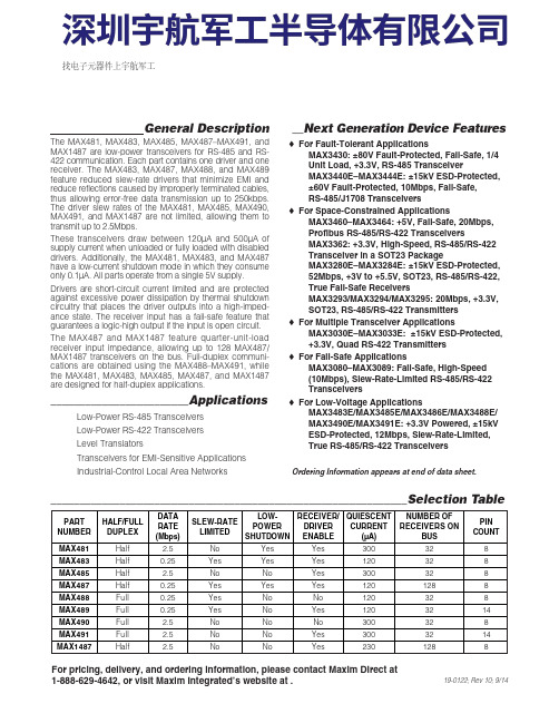
General DescriptionThe MAX481, MAX483, MAX485, MAX487–MAX491, andMAX1487 are low-power transceivers for RS-485 and RS-422 communication. Each part contains one driver and onereceiver. The MAX483, MAX487, MAX488, and MAX489feature reduced slew-rate drivers that minimize E MI andreduce reflections caused by improperly terminated cables,thus allowing error-free data transmission up to 250kbps.The driver slew rates of the MAX481, MAX485, MAX490,MAX491, and MAX1487 are not limited, allowing them totransmit up to 2.5Mbps.These transceivers draw between 120µA and 500µA ofsupply current when unloaded or fully loaded with disableddrivers. Additionally, the MAX481, MAX483, and MAX487have a low-current shutdown mode in which they consumeonly 0.1µA. All parts operate from a single 5V supply.Drivers are short-circuit current limited and are protectedagainst excessive power dissipation by thermal shutdowncircuitry that places the driver outputs into a high-imped-ance state. The receiver input has a fail-safe feature thatguarantees a logic-high output if the input is open circuit.The MAX487 and MAX1487 feature quarter-unit-loadreceiver input impedance, allowing up to 128 MAX487/MAX1487 transceivers on the bus. Full-duplex communi-cations are obtained using the MAX488–MAX491, whilethe MAX481, MAX483, MAX485, MAX487, and MAX1487are designed for half-duplex applications.________________________Applications Low-Power RS-485 Transceivers Low-Power RS-422 Transceivers Level Translators Transceivers for EMI-Sensitive Applications Industrial-Control Local Area Networks__Next Generation Device Features o For Fault-Tolerant Applications MAX3430: ±80V Fault-Protected, Fail-Safe, 1/4Unit Load, +3.3V, RS-485 Transceiver MAX3440E–MAX3444E: ±15kV ESD-Protected,±60V Fault-Protected, 10Mbps, Fail-Safe, RS-485/J1708 Transceivers o For Space-Constrained Applications MAX3460–MAX3464: +5V, Fail-Safe, 20Mbps,Profibus RS-485/RS-422 Transceivers MAX3362: +3.3V, High-Speed, RS-485/RS-422Transceiver in a SOT23 Package MAX3280E–MAX3284E: ±15kV ESD-Protected,52Mbps, +3V to +5.5V, SOT23, RS-485/RS-422,True Fail-Safe Receivers MAX3293/MAX3294/MAX3295: 20Mbps, +3.3V,SOT23, RS-485/RS-422 Transmitters o For Multiple Transceiver Applications MAX3030E–MAX3033E: ±15kV ESD-Protected,+3.3V, Quad RS-422 Transmitters o For Fail-Safe Applications MAX3080–MAX3089: Fail-Safe, High-Speed (10Mbps), Slew-Rate-Limited RS-485/RS-422Transceiverso For Low-Voltage ApplicationsMAX3483E/MAX3485E/MAX3486E/MAX3488E/MAX3490E/MAX3491E: +3.3V Powered, ±15kVESD-Protected, 12Mbps, Slew-Rate-Limited,True RS-485/RS-422 Transceivers For pricing, delivery, and ordering information, please contact Maxim Direct at1-888-629-4642, or visit Maxim Integrated’s website at .______________________________________________________________Selection Table19-0122; Rev 10; 9/14PARTNUMBERHALF/FULL DUPLEX DATA RATE (Mbps) SLEW-RATE LIMITED LOW-POWER SHUTDOWN RECEIVER/DRIVER ENABLE QUIESCENT CURRENT (μA) NUMBER OF RECEIVERS ON BUS PIN COUNT MAX481Half 2.5No Yes Yes 300328MAX483Half 0.25Yes Yes Yes 120328MAX485Half 2.5No No Yes 300328MAX487Half 0.25Yes Yes Yes 1201288MAX488Full 0.25Yes No No 120328MAX489Full 0.25Yes No Yes 1203214MAX490Full 2.5No No No 300328MAX491Full 2.5No No Yes 3003214MAX1487 Half 2.5No No Yes 2301288Ordering Information appears at end of data sheet.找电子元器件上宇航军工MAX481/MAX483/MAX485/MAX487–MAX491/MAX1487Low-Power, Slew-Rate-LimitedRS-485/RS-422 TransceiversPackage Information For the latest package outline information and land patterns, go to . Note that a “+”, “#”, or “-”in the package code indicates RoHS status only. Package drawings may show a different suffix character, but the drawing pertains to the package regardless of RoHS status.16Low-Power, Slew-Rate-Limited RS-485/RS-422 TransceiversMAX481/MAX483/MAX485/MAX487–MAX491/MAX1487Maxim Integrated cannot assume responsibility for use of any circuitry other than circuitry entirely embodied in a Maxim Integrated product. No circuit patent licenses are implied. Maxim Integrated reserves the right to change the circuitry and specifications without notice at any time. The parametric values (min and max limits) shown in the Electrical Characteristics table are guaranteed. Other parametric values quoted in this data sheet are provided for guidance.Maxim Integrated 160 Rio Robles, San Jose, CA 95134 USA 1-408-601-100017©2014 Maxim Integrated Products, Inc.Maxim Integrated and the Maxim Integrated logo are trademarks of Maxim Integrated Products, Inc.。

1、特点z分辨率:14 bitz工作电压:3.3V电源z转换速率:可达210MHzz满量程输出电流可调整范围:2mA~20mAz输入类型:并行输入z工作模式:电流型z功耗:150mW@3.3Vz兼容AD97442、功能描述MXT2144是一种14位电流输出型、CMOS D/A转换器,最大刷新率至少可达200MSPS,工作电压支持3.3伏,在3.3伏电压下工作时功耗小于160毫瓦。
在待机模式下,其功耗约为20mW。
该D/A转换器采用了分段电流沉结构,可以有效的减小电流开关的数量,从而减小开关电流的浪涌,改善建立时间,提高转换器的精度.该D/A转换器主要应用在通讯、仪器仪表、高分辨率图像系统、波形发生器等方面。
该电路在工作时,输入的14位数字信号存放在内部寄存器,然后控制电流源阵列的电流源打开或关断,从而控制电流的增加或减小。
整个电路可以分为电压基准源、偏置电路、电流源阵列、电流开关和高速锁存器等部分。
MXT2144内部寄存器在时钟上升沿进行刷新。
如果驱动时钟或数字输入的线电阻有50Ω,为了减小反射,建议在管脚附近用50Ω电阻接地。
另外,也建议把数字电源与模拟电源,数字地与模拟地分开,以使其性能最优化。
为了减小电源噪声,最好在靠近AVDD和DVDD管脚处分别对模拟地和数字地接0.1uF的电容。
MXT2144内部带隙电压参考源为1.22V,在整个温度范围温度系数为±50ppm/℃。
管脚16 VREFLO是参考选择端,如果VREFLO接地,则为内部参考;若接模拟电源,则为使用外部参考源,由17管脚输入。
输出I OUT的电流由18管脚的FSADJ端所接的R SET来设置,满量程范围为2~20mA可调。
如果采用内部参考,则V FSADJ约为1.22V;如用外部参考,则V FSADJ约等于外参考电压。
满量程输出电流 I OUTFS=(V FSADJ/R SET) X 32当满量程电流为20mA时,输入码与输出电流的对应关系表(表1):表1INPUT CODE(D13-D0) IOUTA(mA) IOUTB(mA)1111 11111 11111 20 01000 00000 00000 10 100000 00000 00000 0 20IOUTA与IOUTB为互补电流输出端,它们的和总是等于满量程电流减去1LSB。

MAX220--MAX249.PDF PAGE14翻译详细说明MAX220–MAX249 包含4个部件:双路电荷泵DC-DC 电压转换器、RS-232 驱动器、RS-232 接收器,以及接收器与发送器使能控制输入。
双路电荷泵电压转换器MAX220–MAX249内部有两个电荷泵,将+5V转换为±10V (空载),为RS-232驱动器提供工作电压。
第一个转换器利用电容C1将+5V 输入加倍,得到V+输出端C3上的+10V.第二个转换器利用电容C2 将+10V转换为V- 输出端C4 上的-10V。
可以从+10V (V+) 和-10V (V-) 输出端获取少量的电量,为外部电路供电( 参见典型工作特性部分) ;但MAX225与MAX245–MAX247例外,因为它们不提供这些引脚。
V+ 与V-未经稳压,所以输出电压会随负载电流的增大而下降。
V +和V -端不稳定,因此,输出电压随着负载电流下降.当V+、V-为外部电路提供电流时,注意不要因为所加负载的原因使V+ 、V- 低于EIA/TIA-232E 驱动器输出电压最小值±5V的限制。
使用MAX222、MAX225、MAX230、MAX235、MAX236、MAX240、MAX241以及MAX245–MAX249上的关断功能时,应避免V+与V-为外部电路供电。
这些器件关断时,V-降至0V,V+降至+5V。
对于那些能够将+10V外部电源提供到V+ 引脚(而不是使用内部电荷泵来产生+10V)的应用,一定不要安装电容C1,并且必须将SHDN 引脚连接至VCC,这是因为在关断模式下V+ 被内部连接到VCC。
RS-232 驱动器如果负载是标称值为5kΩ的RS-232接收器,并且VCC = +5V时,驱动器输出电压摆幅的典型值为±8V 。
输出摆幅确保符合EIA/TIA-232E 和V.28 规范,该规范要求在最糟糕的情况下能够满足±5V驱动器输出电压最小值的要求,其中包括3kΩ的负载电阻最小值,Vcc = +4.5V,以及最高工作温度。


MZ-RS244T使用手册目录MZ-RS244T使用手册 (2)概述: (2)特点: (2)接口: (3)RS485接口和422接口: (3)RS232接口: (3)TTL接口: (3)驱动安装: (7)驱动的获取: (7)安装步骤: (7)规格: (9)赠送软件列表: (11)装货清单: (12)联系我们: (12)技术支持: (12)致谢:很感谢您购买我公司的产品,由于您的支持我公司能够提供更好的产品与服务。
版权声明:本产品本身,包装,软件,说明书,均为本公司所有,均受法律保护。
未经许可严禁转载复制;使用。
如需转载;复制;使用,请经过本公司允许,并说明出处。
------------------------------------------------------------------------------------------------------------------------------------------编写时间:2019-05-08MZ-RS244T使用手册产品名称:USB 多功能转换器产品型号:MZ-RS244T产品尺寸:72X 113 X 23.5(mm)USB 线长: 1 .5米内包装: 蓝色ABS外壳外包装: 纸盒概述:MZ-RS244T可使你在TTL;422(RS-422全双工);485(RS-485半双工);串口(RS-232)和USB接口之间非常容易地建立可靠的连接。
通过利用USB 接口具有的即插即用和热插拔的能力可能给RS-422/485外围设备提供非常容易使用的环境。
它的设计可以让你方便地连接诸如打印机、监控球机、ISDN-TA、Modem等设备还可以用作单片机程序、HEX文件烧录、机顶盒升级,并提供高达1Mbps的传输速率。
特点:●主芯片采用FT232RL;●USB1.1/2.0 兼容的解决方案;●传输速率最高可达1Mbaud;●内建128 byte TX / 384 byte RX 缓存;●支持Windows全系列操作系统;●支持Linux,Mac 系统;●支持全速USB 数据传输协议;------------------------------------------------------------------------------------------------------------------------------------------ TEL:155****9088编写时间:2019-05-08●USB取电,无需外接电源●USB,RS-485接口特别接入自恢复保险●RS-485格式支持半双工,二线制通讯方向自动判别●RS422全双工4线制通讯,同时收发数据●可插拔接线端子,方便易用●抗电磁干扰及电磁辐射的双层PCB 设计;●外观采用清晰指示界面,采用通过UL 认证的连接线缆;●5颗高亮LED指示灯工作状态显示;●可广泛应用于工业仪器、仪表、自动化控制设备与计算机的数据交换。


专业提供塑料加工技术资料:DEMAG 德国德马格注塑机操作手册(中文)FERROMATIK MILACRON 德国RFERROMATI米拉克龙注塑机操作手册(中文或英文)MILACRON 美国米拉克龙注塑机操作手册(中文或英文)MAXIMA 500—MAXIMA1000,HUSKY加拿大赫斯基注塑机操作手册(英文)QUADLOC : Q/QL1350—Q/QL5400<<HUSKY Training Manual>>:加拿大赫斯基注塑机培训手册(英文),由HUSKY比利时工程师提供KRAUSS-MAFFEI 德国克劳斯玛菲注塑机操作手册(德文或英文)KM40C—KM650C, KM800-KM4000KM C-range: KM80-390C1,KM200-1400C2+,KM320-1900C3KM CX-series: KM35-SP180CX, KM160-SP750CXMC series: KM800-8100,KM1300-8100, KM2300-17200克劳斯玛菲工程师提供的注塑机技术培训手册:(均为英文和德文)<<Manual Controller Technology MC5 Maintenance and Fault Rectification in the MC5 System>>: 516 pages<<Manual Controller Technology MC4 Maintenance and Fault Rectification in the MC4 System>>: 326 pages<<Manual Controller Technology MC3F Maintenance and Fault Rectification in the MC3F System>>: 350 pages<<Control Technology MC3F Training Manual>>: 205 pages<<MC3F Operating and Maintenance Instruction>>: 492 pages<<KM C-Range/MC-Range/CX-Range/MX-Range Hydraulic Manual>>: 170pages/245pages/244pages/425pagesBEKUM奥地利贝克姆吹塑机操作手册(英文)BEKUM BA 62ABB机器人(英文)《ABB机器人S4P+培训手册》(英文)KUKA德国库卡机器人(中、英、德文)KUKA机器人培训教材(中英对照)REMAK德国REMAK机械手(英文)克劳斯玛菲注塑机专用机械手操作手册<<Service Manual for Robot LR-Series>>德国BRANSON必能信震动焊接机操作手册(英文)<<BRANSON Vibration Welding System>>德国KLN超声波焊接机操作手册(英文)<<KLN Ultrasonic Generator Manual>>还提供以上机器的电路图,液压图及气路图。

目錄版權聲明 (i)1. 產品介紹 (ii)1.1 印表機簡介................................................................................................ i i1.2 安規認證.................................................................................................... i i2. 入門 (1)2.1 拆封及檢查 (1)2.2 印表機組件 (2)2.2.1 外觀 (2)2.2.2 內部 (4)2.2.3 後部 (5)3. 安裝 (6)3.1 安裝印表機 (6)3.2 開啟/關閉上蓋 (7)3.3 安裝碳帶 (8)3.4 安裝標籤 (11)3.4.1 安裝標籤 (11)3.4.2 安裝外部進紙標籤(選配) (13)3.4.3 剝紙模式裝紙(選配) (15)3.4.4裁刀模式裝紙(選配) (17)3.5 印表機診斷工具(Diagnostic Tool) (18)3.5.1 啟用Diagnostic Tool工具程式 (18)3.5.2 印表機組態設定(感應器校正、設定乙太網路、設定印表機RTC時間參數.........) (19)3.6. 用印表機診斷工具(Diagnostic Tool)設定乙太網路 (20)3.6.1 經由USB介面設定 (20)3.6.2經由RS-232介面設定 (21)3.6.3 經由Ethernet介面設定 (22)3.7 安裝SD記憶卡 (24)4. LED指示燈及按鍵功能 (26)4.1 LED指示燈 (26)4.2 一般按鍵功能 (26)4.3 開機功能 (27)4.3.1 偵測碳帶強度;間隙/黑標感應器偵測 (27)4.3.2間隙/黑標感應器偵測;列印自測值並進入除錯模式 (28)4.3.3 印表機初始化 (31)4.3.4選用並校正黑標感應器 (32)4.3.5 選用校正間隙感應器 (33)4.3.6 跳過AUTO.BAS程式 (33)5. 故障排除 (34)5.1 LED指示燈狀態 (34)5.2 列印品質 (35)6. 保養 (36)更新記錄 (38)版權聲明本文件所收錄之資訊如有更動本公司不再另行通知。


74LCX244 — Low Voltage Buffer/Line Driver with 5V Tolerant Inputs and OutputsLow Voltage Buffer/Line Driver with 5V Tolerant Inputs and OutputsFeatures■ 5V tolerant inputs and outputs■ 2.3V to 3.6V V CC specifications provided ■ 6.5ns t PD max. (V CC = 3.3V), 10µA I CC max. ■ Power down high impedance inputs and outputs ■ Supports live insertion/withdrawal (1) ■ ±24mA output drive (V CC = 3.0V)■ Implements patented noise/EMI reduction circuitry ■ Latch-up performance exceeds 500mA ■ ESD performance:– Human body model >2000V – Machine model > 200V ■ Leadless DQFN packageNote:1.To ensure the high-impedance state during power up or down, OE should be tied to V CC through a pull-up resistor: the minimum value or the resistor isdetermined by the current-sourcing capability of the driver.General DescriptionThe LCX244 contains eight non-inverting buffers with 3-STATE outputs. The device may be employed as a memory address driver, clock driver and bus-oriented transmitter/receiver. The LCX244 is designed for low voltage (2.5V or 3.3V) V CC applications with capability of interfacing to a 5V signal environment.The LCX244 is fabricated with an advanced CMOS tech-nology to achieve high speed operation while maintain-ing CMOS low power dissipation.Ordering InformationNote:Order NumberPackage NumberPackage Description74LCX244WM M20B 20-Lead Small Outline Integrated Circuit (SOIC), JEDEC MS-013, 0.300" Wide 74LCX244SJ M20D 20-Lead Small Outline Package (SOP), EIAJ TYPE II, 5.3mm Wide 74LCX244BQX (2)MLP20B 20-Terminal Depopulated Quad Very-Thin Flat Pack No Leads (DQFN), JEDEC MO-241, 2.5 x 4.5mm74LCX244MSA MSA2020-Lead Shrink Small Outline Package (SSOP), JEDEC MO-150, 5.3mm Wide 74LCX244MTCMTC2020-Lead Thin Shrink Small Outline Package (TSSOP), JEDEC MO-153, 4.4mm Wide元器件交易网(Top Through View) Pin Description Truth TablesH = HIGH Voltage Level L = LOW Voltage Level X = ImmaterialZ = High ImpedancePin Names DescriptionOE1, OE23-STATE Output Enable Inputs I0–I7InputsO0–O7OutputsInputs OutputsOE1I n(Pins 12, 14, 16, 18) L L HL H LH X ZInputs OutputsOE2I n(Pins 3, 5, 7, 9)L L HL H LH X Z元器件交易网74LCX244 — Low Voltage Buffer/Line Driver with 5V Tolerant Inputs and Outputs Pad Assignments for DQFN74LCX244 — Low Voltage Buffer/Line Driver with 5V Tolerant Inputs and OutputsNote:3.I O Absolute Maximum Rating must be observed.Recommended Operating Conditions (4)The Recommended Operating Conditions table defines the conditions for actual device operation. Recommended operating conditions are specified to ensure optimal performance to the datasheet specifications. Fairchild does not recommend exceeding them or designing to absolute maximum ratings.V CC Supply Voltage –0.5V to +7.0V V I DC Input Voltage –0.5V to +7.0V V ODC Output Voltage Output in 3-STATE–0.5V to +7.0V Output in HIGH or LOW State (3)–0.5V to V CC + 0.5VI IK DC Input Diode Current, V I < GND –50mA I OKDC Output Diode Current V O < GND –50mA V O > V CC+50mA I O DC Output Source/Sink Current ±50mA I CC DC Supply Current per Supply Pin ±100mA I GND DC Ground Current per Ground Pin ±100mAT STGStorage Temperature–65°C to +150°CSymbolParameter Min.Max.UnitsV CCSupply Voltage Operating 2.0 3.6V Data Retention1.5 3.6V I Input Voltage 0 5.5V V OOutput Voltage 3-STATE0 5.5VHIGH or LOW StateV CC I OH / I OLOutput Current V CC = 3.0V–3.6V ±24mAV CC = 2.7V–3.0V ±12 V CC = 2.3V–2.7V±8T A Free-Air Operating Temperature–4085°C ∆ t / ∆ VInput Edge Rate, V IN = 0.8V–2.0V , V CC = 3.0V10ns /V元器件交易网74LCX244 — Low Voltage Buffer/Line Driver with 5V Tolerant Inputs and OutputsNote:5.Outputs disabled or 3-STATE only.AC Electrical CharacteristicsNote:6.Skew is defined as the absolute value of the difference between the actual propagation delay for any two separate V IL LOW Level Input Voltage 2.3–2.70.7V 2.7–3.60.8V OHHIGH Level Output Voltage2.3–3.6I OH = –100µA V CC – 0.2V2.3I OH = –8mA 1.82.7I OH = –12mA 2.23.0I OH = –18mA 2.4I OH = –24mA 2.2V OLLOW Level Output Voltage 2.3–3.6I OL = 100µA 0.2V2.3I OL = 8mA 0.62.7I OL =12mA 0.43.0I OL = 16mA 0.4I OL = 24mA 0.55I I Input Leakage Current 2.3–3.60 ≤ V I ≤ 5.5V ±5.0µA I OZ 3-STATE Output Leakage 2.3–3.60 ≤ V O ≤ 5.5V , V I = V IH or V IL ±5.0µA I OFF Power-Off Leakage Current 0V I or V O = 5.5V 10µA I CC Quiescent Supply Current 2.3–3.6V I = V CC or GND 10µA 3.6V ≤ V I , V O ≤ 5.5V (5)±10∆I CCIncrease in I CC per Input2.3–3.6V IH = V CC – 0.6V500µASymbolParameterT A = –40°C to +85°C, R L = 500ΩUnitsV CC = 3.3V ± 0.3V,C L = 50pFV CC = 2.7V,C L = 50pF V CC = 2.5V ± 0.2V,C L = 30pF Min.Max.Min.Max.Min.Max.t PHL , t PLH Propagation Delay, Data to Output 1.5 6.5 1.57.5 1.57.8ns t PZL , t PZH Output Enable Time 1.58.0 1.59.0 1.510.0ns t PLZ , t PHZ Output Disable Time 1.57.0 1.58.01.58.4ns t OSHL , t OSLHOutput to Output Skew (6)1.0ns元器件交易网74LCX244 — Low Voltage Buffer/Line Driver with 5V Tolerant Inputs and OutputsCapacitanceV OLVQuiet Output Dynamic Valley V OL3.3C L = 50pF , V IH = 3.3V , V IL = 0V –0.8V2.5C L = 30pF , V IH = 2.5V , V IL = 0V–0.6SymbolParameterConditionsTypicalUnitsC IN Input Capacitance V CC = Open, V I = 0V or V CC 7.0pF C OUT Output CapacitanceV CC = 3.3V , V I = 0V or V CC8.0pF C PDPower Dissipation CapacitanceV CC = 3.3V , V I = 0V or V CC , f = 10MHz25.0pF3-STATE Output Low Enable andDisable Times for Logict rise and t fallSymbolV CC3.3V ± 0.3V 2.7V 2.5V ± 0.2VV mi 1.5V 1.5V V CC /2V mo 1.5V 1.5V V CC /2V V + 0.3V V + 0.3V V + 0.15VReel Dimensions inches (millimeters)Figure 3. 20-Lead Small Outline Integrated Circuit (SOIC), JEDEC MS-013, 0.300" WidePackage drawings are provided as a service to customers considering Fairchild components. Drawings may change in any manner without notice. Please note the revision and/or date on the drawing and contact a Fairchild Semiconductor representative to verify or obtain the most recent revision. Package specifications do not expand the terms of Fairchild’s worldwide terms and conditions, specifically the warranty therein, which covers Fairchild products.Always visit Fairchild Semiconductor’s online packaging area for the most recent package drawings:/packaging/DETAIL ASCALE:2:1F)DRAWING FILENAME:MKT-M20BREV3(1.40)Figure 4. 20-Lead Small Outline Package (SOP), EIAJ TYPE II, 5.3mm WidePackage drawings are provided as a service to customers considering Fairchild components. Drawings may change in any manner without notice. Please note the revision and/or date on the drawing and contact a Fairchild Semiconductor representative to verify orFigure 5. 20-Terminal Depopulated Quad Very-Thin Flat Pack No Leads (DQFN), JEDEC MO-241, 2.5 x 4.5mm Package drawings are provided as a service to customers considering Fairchild components. Drawings may change in any mannerFigure 6. 20-Lead Shrink Small Outline Package (SSOP), JEDEC MO-150, 5.3mm WidePackage drawings are provided as a service to customers considering Fairchild components. Drawings may change in any manner without notice. Please note the revision and/or date on the drawing and contact a Fairchild Semiconductor representative to verify or obtain the most recent revision. Package specifications do not expand the terms of Fairchild’s worldwide terms and conditions,Figure 7. 20-Lead Thin Shrink Small Outline Package (TSSOP), JEDEC MO-153, 4.4mm WidePackage drawings are provided as a service to customers considering Fairchild components. Drawings may change in any mannersubsidiaries,and is not intended to be an exhaustive list of all such trademarks.ACEx®Build it Now™CorePLUS™CROSSVOLT™CTL™Current Transfer Logic™EcoSPARK®EZSWITCH™*™®Fairchild®Fairchild Semiconductor®FACT Quiet Series™FACT®FAST®FastvCore™FlashWriter®*FPS™FRFET®Global Power Resource SMGreen FPS™Green FPS™e-Series™GTO™i-Lo™IntelliMAX™ISOPLANAR™MegaBuck™MICROCOUPLER™MicroFET™MicroPak™MillerDrive™Motion-SPM™OPTOLOGIC®OPTOPLANAR®®PDP-SPM™Power220®POWEREDGE®Power-SPM™PowerTrench®Programmable Active Droop™QFET®QS™QT Optoelectronics™Quiet Series™RapidConfigure™SMART START™SPM®STEALTH™SuperFET™SuperSOT™-3SuperSOT™-6SuperSOT™-8SupreMOS™SyncFET™®The Power Franchise®TinyBoost™TinyBuck™TinyLogic®TINYOPTO™TinyPower™TinyPWM™TinyWire™µSerDes™UHC®Ultra FRFET™UniFET™VCX™*EZSWITCH™and FlashWriter®are trademarks of System General Corporation,used under license by Fairchild Semiconductor.DISCLAIMERFAIRCHILD SEMICONDUCTOR RESERVES THE RIGHT TO MAKE CHANGES WITHOUT FURTHER NOTICE TO ANY PRODUCTS HEREIN TO IMPROVE RELIABILITY,FUNCTION,OR DESIGN.FAIRCHILD DOES NOT ASSUME ANY LIABILITY ARISING OUT OF THE APPLICATION OR USE OF ANY PRODUCT OR CIRCUIT DESCRIBED HEREIN;NEITHER DOES IT CONVEY ANY LICENSE UNDER ITS PATENT RIGHTS,NOR THE RIGHTS OF OTHERS.THESE SPECIFICATIONS DO NOT EXPAND THE TERMS OF FAIRCHILD’S WORLDWIDE TERMS AND CONDITIONS,SPECIFICALLY THE WARRANTY THEREIN,WHICH COVERS THESE PRODUCTS.LIFE SUPPORT POLICYFAIRCHILD’S PRODUCTS ARE NOT AUTHORIZED FOR USE AS CRITICAL COMPONENTS IN LIFE SUPPORT DEVICES OR SYSTEMS WITHOUT THE EXPRESS WRITTEN APPROVAL OF FAIRCHILD SEMICONDUCTOR CORPORATION.As used herein:1.Life support devices or systems are devices or systemswhich,(a)are intended for surgical implant into the body or(b)support or sustain life,and(c)whose failure to performwhen properly used in accordance with instructions for use provided in the labeling,can be reasonably expected to result in a significant injury of the user.2.A critical component in any component of a life support,device,or system whose failure to perform can be reasonably expected to cause the failure of the life support device or system,or to affect its safety or effectiveness.PRODUCT STATUS DEFINITIONSDefinition of TermsDatasheet Identification Product Status DefinitionAdvance Information Formative or In Design This datasheet contains the design specifications for product development.Specifications may change in any manner without notice.Preliminary First Production This datasheet contains preliminary data;supplementary data will bepublished at a later date.Fairchild Semiconductor reserves the right tomake changes at any time without notice to improve design. 74LCX244 — Low Voltage Buffer/Line Driver with 5V Tolerant Inputs and Outputs。
General DescriptionThe MAX220–MAX249 family of line drivers/receivers is intended for all EIA/TIA-232E and V.28/V.24 communica-tions interfaces, particularly applications where ±12V is not available.These parts are especially useful in battery-powered sys-tems, since their low-power shutdown mode reduces power dissipation to less than 5µW. The MAX225,MAX233, MAX235, and MAX245/MAX246/MAX247 use no external components and are recommended for appli-cations where printed circuit board space is critical.________________________ApplicationsPortable Computers Low-Power Modems Interface TranslationBattery-Powered RS-232 Systems Multidrop RS-232 NetworksNext-Generation Device Features♦For Low-Voltage, Integrated ESD ApplicationsMAX3222E/MAX3232E/MAX3237E/MAX3241E/MAX3246E: +3.0V to +5.5V, Low-Power, Up to 1Mbps, True RS-232 Transceivers Using Four 0.1µF External Capacitors (MAX3246E Available in a UCSP™Package)♦For Low-Cost ApplicationsMAX221E: ±15kV ESD-Protected, +5V, 1µA,Single RS-232 Transceiver with AutoShutdown™MAX220–MAX249+5V-Powered, Multichannel RS-232Drivers/Receivers________________________________________________________________Maxim Integrated Products 1Selection Table19-4323; Rev 15; 1/06Power No. of NominalSHDN RxPart Supply RS-232No. of Cap. Value & Three-Active in Data Rate Number (V)Drivers/Rx Ext. Caps (µF)State SHDN (kbps)FeaturesMAX220+52/240.047/0.33No —120Ultra-low-power, industry-standard pinout MAX222+52/2 4 0.1Yes —200Low-power shutdownMAX223 (MAX213)+54/54 1.0 (0.1)Yes ✔120MAX241 and receivers active in shutdown MAX225+55/50—Yes ✔120Available in SOMAX230 (MAX200)+55/04 1.0 (0.1)Yes —120 5 drivers with shutdownMAX231 (MAX201)+5 and2/2 2 1.0 (0.1)No —120Standard +5/+12V or battery supplies; +7.5 to +13.2same functions as MAX232MAX232 (MAX202)+52/24 1.0 (0.1)No —120 (64)Industry standardMAX232A+52/240.1No —200Higher slew rate, small caps MAX233 (MAX203)+52/20— No —120No external capsMAX233A+52/20—No —200No external caps, high slew rate MAX234 (MAX204)+54/04 1.0 (0.1)No —120Replaces 1488MAX235 (MAX205)+55/50—Yes —120No external capsMAX236 (MAX206)+54/34 1.0 (0.1)Yes —120Shutdown, three stateMAX237 (MAX207)+55/34 1.0 (0.1)No —120Complements IBM PC serial port MAX238 (MAX208)+54/44 1.0 (0.1)No —120Replaces 1488 and 1489MAX239 (MAX209)+5 and3/52 1.0 (0.1)No —120Standard +5/+12V or battery supplies;+7.5 to +13.2single-package solution for IBM PC serial port MAX240+55/54 1.0Yes —120DIP or flatpack package MAX241 (MAX211)+54/54 1.0 (0.1)Yes —120Complete IBM PC serial port MAX242+52/240.1Yes ✔200Separate shutdown and enableMAX243+52/240.1No —200Open-line detection simplifies cabling MAX244+58/104 1.0No —120High slew rateMAX245+58/100—Yes ✔120High slew rate, int. caps, two shutdown modes MAX246+58/100—Yes ✔120High slew rate, int. caps, three shutdown modes MAX247+58/90—Yes ✔120High slew rate, int. caps, nine operating modes MAX248+58/84 1.0Yes ✔120High slew rate, selective half-chip enables MAX249+56/1041.0Yes✔120Available in quad flatpack packageFor pricing, delivery, and ordering information,please contact Maxim/Dallas Direct!at 1-888-629-4642, or visit Maxim’s website at .Ordering InformationOrdering Information continued at end of data sheet.*Contact factory for dice specifications.AutoShutdown and UCSP are trademarks of Maxim Integrated Products, Inc.M A X 220–M A X 249+5V-Powered, Multichannel RS-232Drivers/Receivers 2_______________________________________________________________________________________ABSOLUTE MAXIMUM RATINGS—MAX220/222/232A/233A/242/243ELECTRICAL CHARACTERISTICS—MAX220/222/232A/233A/242/243Note 1:For the MAX220, V+ and V- can have a maximum magnitude of 7V, but their absolute difference cannot exceed 13V.Note 2:Input voltage measured with T OUT in high-impedance state, SHDN or V CC = 0V.Note 3:Maximum reflow temperature for the MAX233A is +225°C.Stresses beyond those listed under “Absolute Maximum Ratings” may cause permanent damage to the device. These are stress ratings only, and functional operation of the device at these or any other conditions beyond those indicated in the operational sections of the specifications is not implied. Exposure to absolute maximum rating conditions for extended periods may affect device reliability.Supply Voltage (V CC )...............................................-0.3V to +6V V+ (Note 1)..................................................(V CC - 0.3V) to +14V V- (Note 1).............................................................+0.3V to +14V Input VoltagesT IN ..............................................................-0.3V to (V CC - 0.3V)R IN (Except MAX220)........................................................±30V R IN (MAX220).....................................................................±25V T OUT (Except MAX220) (Note 2).......................................±15V T OUT (MAX220)...............................................................±13.2V Output VoltagesT OUT ...................................................................................±15V R OUT .........................................................-0.3V to (V CC + 0.3V)Driver/Receiver Output Short Circuited to GND.........Continuous Continuous Power Dissipation (T A = +70°C)16-Pin Plastic DIP (derate 10.53mW/°C above +70°C)..842mW18-Pin Plastic DIP (derate 11.11mW/°C above +70°C)..889mW 20-Pin Plastic DIP (derate 8.00mW/°C above +70°C)..440mW 16-Pin Narrow SO (derate 8.70mW/°C above +70°C)...696mW 16-Pin Wide SO (derate 9.52mW/°C above +70°C)......762mW 18-Pin Wide SO (derate 9.52mW/°C above +70°C)......762mW 20-Pin Wide SO (derate 10.00mW/°C above +70°C)....800mW 20-Pin SSOP (derate 8.00mW/°C above +70°C)..........640mW 16-Pin CERDIP (derate 10.00mW/°C above +70°C).....800mW 18-Pin CERDIP (derate 10.53mW/°C above +70°C).....842mW Operating Temperature RangesMAX2_ _AC_ _, MAX2_ _C_ _.............................0°C to +70°C MAX2_ _AE_ _, MAX2_ _E_ _..........................-40°C to +85°C MAX2_ _AM_ _, MAX2_ _M_ _.......................-55°C to +125°C Storage Temperature Range.............................-65°C to +160°C Lead Temperature (soldering, 10s) (Note 3)...................+300°CMAX220–MAX249+5V-Powered, Multichannel RS-232Drivers/Receivers_______________________________________________________________________________________3Note 4:MAX243 R2OUT IN ELECTRICAL CHARACTERISTICS—MAX220/222/232A/233A/242/243 (continued)M A X 220–M A X 249+5V-Powered, Multichannel RS-232Drivers/Receivers 4_________________________________________________________________________________________________________________________________Typical Operating CharacteristicsMAX220/MAX222/MAX232A/MAX233A/MAX242/MAX243108-1051525OUTPUT VOLTAGE vs. LOAD CURRENT-4-6-8-2642LOAD CURRENT (mA)O U T P U T V O L T A G E (V )1002011104104060AVAILABLE OUTPUT CURRENTvs. DATA RATE65798DATA RATE (kb/s)O U T P U T C U R R E N T (m A )203050+10V-10VMAX222/MAX242ON-TIME EXITING SHUTDOWN+5V +5V 0V0V 500μs/div V +, V - V O L T A G E (V )ELECTRICAL CHARACTERISTICS—MAX220/222/232A/233A/242/243 (continued)(V CC = +5V ±10%, C1–C4 = 0.1µF‚ MAX220, C1 = 0.047µF, C2–C4 = 0.33µF, T A = T MIN to T MAX ‚ unless otherwise noted.)MAX220–MAX249+5V-Powered, Multichannel RS-232Drivers/Receivers_______________________________________________________________________________________5V CC ...........................................................................-0.3V to +6V V+................................................................(V CC - 0.3V) to +14V V-............................................................................+0.3V to -14V Input VoltagesT IN ............................................................-0.3V to (V CC + 0.3V)R IN ......................................................................................±30V Output VoltagesT OUT ...................................................(V+ + 0.3V) to (V- - 0.3V)R OUT .........................................................-0.3V to (V CC + 0.3V)Short-Circuit Duration, T OUT ......................................Continuous Continuous Power Dissipation (T A = +70°C)14-Pin Plastic DIP (derate 10.00mW/°C above +70°C)....800mW 16-Pin Plastic DIP (derate 10.53mW/°C above +70°C)....842mW 20-Pin Plastic DIP (derate 11.11mW/°C above +70°C)....889mW 24-Pin Narrow Plastic DIP(derate 13.33mW/°C above +70°C)..........1.07W24-Pin Plastic DIP (derate 9.09mW/°C above +70°C)......500mW 16-Pin Wide SO (derate 9.52mW/°C above +70°C).........762mW20-Pin Wide SO (derate 10.00mW/°C above +70°C).......800mW 24-Pin Wide SO (derate 11.76mW/°C above +70°C).......941mW 28-Pin Wide SO (derate 12.50mW/°C above +70°C) .............1W 44-Pin Plastic FP (derate 11.11mW/°C above +70°C).....889mW 14-Pin CERDIP (derate 9.09mW/°C above +70°C)..........727mW 16-Pin CERDIP (derate 10.00mW/°C above +70°C)........800mW 20-Pin CERDIP (derate 11.11mW/°C above +70°C)........889mW 24-Pin Narrow CERDIP(derate 12.50mW/°C above +70°C)..............1W24-Pin Sidebraze (derate 20.0mW/°C above +70°C)..........1.6W 28-Pin SSOP (derate 9.52mW/°C above +70°C).............762mW Operating Temperature RangesMAX2 _ _ C _ _......................................................0°C to +70°C MAX2 _ _ E _ _...................................................-40°C to +85°C MAX2 _ _ M _ _......................................................-55°C to +125°C Storage Temperature Range.............................-65°C to +160°C Lead Temperature (soldering, 10s) (Note 4)...................+300°CABSOLUTE MAXIMUM RATINGS—MAX223/MAX230–MAX241ELECTRICAL CHARACTERISTICS—MAX223/MAX230–MAX241(MAX223/230/232/234/236/237/238/240/241, V CC = +5V ±10; MAX233/MAX235, V CC = 5V ±5%‚ C1–C4 = 1.0µF; MAX231/MAX239,V CC = 5V ±10%; V+ = 7.5V to 13.2V; T A = T MIN to T MAX ; unless otherwise noted.)Stresses beyond those listed under “Absolute Maximum Ratings” may cause permanent damage to the device. These are stress ratings only, and functional operation of the device at these or any other conditions beyond those indicated in the operational sections of the specifications is not implied. Exposure to absolute maximum rating conditions for extended periods may affect device reliability.Note 4:Maximum reflow temperature for the MAX233/MAX235 is +225°C.M A X 220–M A X 249+5V-Powered, Multichannel RS-232Drivers/Receivers 6_______________________________________________________________________________________ELECTRICAL CHARACTERISTICS—MAX223/MAX230–MAX241 (continued)(MAX223/230/232/234/236/237/238/240/241, V CC = +5V ±10; MAX233/MAX235, V CC = 5V ±5%‚ C1–C4 = 1.0µF; MAX231/MAX239,V CC = 5V ±10%; V+ = 7.5V to 13.2V; T A = T MIN to T MAX ; unless otherwise noted.)MAX220–MAX249+5V-Powered, Multichannel RS-232Drivers/Receivers_______________________________________________________________________________________78.56.54.55.5TRANSMITTER OUTPUT VOLTAGE (V OH ) vs. V CC7.08.0V CC (V)V O H (V )5.07.57.46.02500TRANSMITTER OUTPUT VOLTAGE (V OH )vs. LOAD CAPACITANCE AT DIFFERENT DATA RATES6.46.27.27.0LOAD CAPACITANCE (pF)V O H (V )1500100050020006.86.612.04.02500TRANSMITTER SLEW RATE vs. LOAD CAPACITANCE6.05.011.09.010.0LOAD CAPACITANCE (pF)S L E W R A T E (V /μs )1500100050020008.07.0-6.0-9.04.55.5TRANSMITTER OUTPUT VOLTAGE (V OL ) vs. V CC-8.0-8.5-6.5-7.0V CC (V)V O L (V )5.0-7.5-6.0-7.62500TRANSMITTER OUTPUT VOLTAGE (V OL )vs. LOAD CAPACITANCE AT DIFFERENT DATA RATES-7.0-7.2-7.4-6.2-6.4LOAD CAPACITANCE (pF)V O L (V )150010005002000-6.6-6.810-105101520253035404550TRANSMITTER OUTPUT VOLTAGE (V+, V-)vs. LOAD CURRENT-2-6-4-886CURRENT (mA)V +, V - (V )420__________________________________________Typical Operating CharacteristicsMAX223/MAX230–MAX241*SHUTDOWN POLARITY IS REVERSED FOR NON MAX241 PARTSV+, V- WHEN EXITING SHUTDOWN(1μF CAPACITORS)MAX220-13SHDN*V-O V+500ms/divM A X 220–M A X 249+5V-Powered, Multichannel RS-232Drivers/Receivers 8_______________________________________________________________________________________ABSOLUTE MAXIMUM RATINGS—MAX225/MAX244–MAX249ELECTRICAL CHARACTERISTICS—MAX225/MAX244–MAX249(MAX225, V CC = 5.0V ±5%; MAX244–MAX249, V CC = +5.0V ±10%, external capacitors C1–C4 = 1µF; T A = T MIN to T MAX ; unless oth-erwise noted.)Stresses beyond those listed under “Absolute Maximum Ratings” may cause permanent damage to the device. These are stress ratings only, and functional operation of the device at these or any other conditions beyond those indicated in the operational sections of the specifications is not implied. Exposure to absolute maximum rating conditions for extended periods may affect device reliability.Supply Voltage (V CC )...............................................-0.3V to +6V Input VoltagesT IN ‚ ENA , ENB , ENR , ENT , ENRA ,ENRB , ENTA , ENTB ..................................-0.3V to (V CC + 0.3V)R IN .....................................................................................±25V T OUT (Note 5).....................................................................±15V R OUT ........................................................-0.3V to (V CC + 0.3V)Short Circuit (one output at a time)T OUT to GND............................................................Continuous R OUT to GND............................................................ContinuousContinuous Power Dissipation (T A = +70°C)28-Pin Wide SO (derate 12.50mW/°C above +70°C).............1W 40-Pin Plastic DIP (derate 11.11mW/°C above +70°C)...611mW 44-Pin PLCC (derate 13.33mW/°C above +70°C)...........1.07W Operating Temperature RangesMAX225C_ _, MAX24_C_ _ ..................................0°C to +70°C MAX225E_ _, MAX24_E_ _ ...............................-40°C to +85°C Storage Temperature Range.............................-65°C to +160°C Lead Temperature (soldering,10s) (Note 6)....................+300°CNote 5:Input voltage measured with transmitter output in a high-impedance state, shutdown, or V CC = 0V.Note 6:Maximum reflow temperature for the MAX225/MAX245/MAX246/MAX247 is +225°C.MAX220–MAX249+5V-Powered, Multichannel RS-232Drivers/Receivers_______________________________________________________________________________________9Note 7:The 300Ωminimum specification complies with EIA/TIA-232E, but the actual resistance when in shutdown mode or V CC =0V is 10M Ωas is implied by the leakage specification.ELECTRICAL CHARACTERISTICS—MAX225/MAX244–MAX249 (continued)(MAX225, V CC = 5.0V ±5%; MAX244–MAX249, V CC = +5.0V ±10%, external capacitors C1–C4 = 1µF; T A = T MIN to T MAX ; unless oth-erwise noted.)M A X 220–M A X 249+5V-Powered, Multichannel RS-232Drivers/Receivers 10________________________________________________________________________________________________________________________________Typical Operating CharacteristicsMAX225/MAX244–MAX24918212345TRANSMITTER SLEW RATE vs. LOAD CAPACITANCE86416LOAD CAPACITANCE (nF)T R A N S M I T T E R S L E W R A T E (V /μs )14121010-105101520253035OUTPUT VOLTAGEvs. LOAD CURRENT FOR V+ AND V--2-4-6-88LOAD CURRENT (mA)O U T P U T V O L T A G E (V )64209.05.012345TRANSMITTER OUTPUT VOLTAGE (V+, V-)vs. LOAD CAPACITANCE AT DIFFERENT DATA RATES6.05.58.5LOAD CAPACITANCE (nF)V +, V (V )8.07.57.06.5MAX220–MAX249Drivers/ReceiversFigure 1. Transmitter Propagation-Delay Timing Figure 2. Receiver Propagation-Delay TimingFigure 3. Receiver-Output Enable and Disable Timing Figure 4. Transmitter-Output Disable TimingM A X 220–M A X 249Drivers/Receivers ENT ENR OPERATION STATUS TRANSMITTERSRECEIVERS00Normal Operation All Active All Active 01Normal Operation All Active All 3-State10Shutdown All 3-State All Low-Power Receive Mode 11ShutdownAll 3-StateAll 3-StateTable 1a. MAX245 Control Pin ConfigurationsENT ENR OPERATION STATUS TRANSMITTERS RECEIVERSTA1–TA4TB1–TB4RA1–RA5RB1–RB500Normal Operation All Active All Active All Active All Active 01Normal Operation All Active All Active RA1–RA4 3-State,RA5 Active RB1–RB4 3-State,RB5 Active 1ShutdownAll 3-StateAll 3-StateAll Low-Power Receive Mode All Low-Power Receive Mode 11Shutdown All 3-State All 3-StateRA1–RA4 3-State,RA5 Low-Power Receive ModeRB1–RB4 3-State,RB5 Low-Power Receive ModeTable 1b. MAX245 Control Pin ConfigurationsTable 1c. MAX246 Control Pin ConfigurationsENA ENB OPERATION STATUS TRANSMITTERS RECEIVERSTA1–TA4TB1–TB4RA1–RA5RB1–RB500Normal Operation All Active All Active All Active All Active 01Normal Operation All Active All 3-State All Active RB1–RB4 3-State,RB5 Active 1ShutdownAll 3-StateAll ActiveRA1–RA4 3-State,RA5 Active All Active 11Shutdown All 3-State All 3-StateRA1–RA4 3-State,RA5 Low-Power Receive ModeRB1–RB4 3-State,RA5 Low-Power Receive ModeMAX220–MAX249Drivers/ReceiversM A X 220–M A X 249_______________Detailed DescriptionThe MAX220–MAX249 contain four sections: dual charge-pump DC-DC voltage converters, RS-232 dri-vers, RS-232 receivers, and receiver and transmitter enable control inputs.Dual Charge-Pump Voltage ConverterThe MAX220–MAX249 have two internal charge-pumps that convert +5V to ±10V (unloaded) for RS-232 driver operation. The first converter uses capacitor C1 to dou-ble the +5V input to +10V on C3 at the V+ output. The second converter uses capacitor C2 to invert +10V to -10V on C4 at the V- output.A small amount of power may be drawn from the +10V (V+) and -10V (V-) outputs to power external circuitry (see the Typical Operating Characteristics section),except on the MAX225 and MAX245–MAX247, where these pins are not available. V+ and V- are not regulated,so the output voltage drops with increasing load current.Do not load V+ and V- to a point that violates the mini-mum ±5V EIA/TIA-232E driver output voltage when sourcing current from V+ and V- to external circuitry. When using the shutdown feature in the MAX222,MAX225, MAX230, MAX235, MAX236, MAX240,MAX241, and MAX245–MAX249, avoid using V+ and V-to power external circuitry. When these parts are shut down, V- falls to 0V, and V+ falls to +5V. For applica-tions where a +10V external supply is applied to the V+pin (instead of using the internal charge pump to gen-erate +10V), the C1 capacitor must not be installed and the SHDN pin must be tied to V CC . This is because V+is internally connected to V CC in shutdown mode.RS-232 DriversThe typical driver output voltage swing is ±8V when loaded with a nominal 5k ΩRS-232 receiver and V CC =+5V. Output swing is guaranteed to meet the EIA/TIA-232E and V.28 specification, which calls for ±5V mini-mum driver output levels under worst-case conditions.These include a minimum 3k Ωload, V CC = +4.5V, and maximum operating temperature. Unloaded driver out-put voltage ranges from (V+ -1.3V) to (V- +0.5V).Input thresholds are both TTL and CMOS compatible.The inputs of unused drivers can be left unconnected since 400k Ωinput pullup resistors to V CC are built in (except for the MAX220). The pullup resistors force the outputs of unused drivers low because all drivers invert.The internal input pullup resistors typically source 12µA,except in shutdown mode where the pullups are dis-abled. Driver outputs turn off and enter a high-imped-ance state—where leakage current is typically microamperes (maximum 25µA)—when in shutdownmode, in three-state mode, or when device power is removed. Outputs can be driven to ±15V. The power-supply current typically drops to 8µA in shutdown mode.The MAX220 does not have pullup resistors to force the outputs of the unused drivers low. Connect unused inputs to GND or V CC .The MAX239 has a receiver three-state control line, and the MAX223, MAX225, MAX235, MAX236, MAX240,and MAX241 have both a receiver three-state control line and a low-power shutdown control. Table 2 shows the effects of the shutdown control and receiver three-state control on the receiver outputs.The receiver TTL/CMOS outputs are in a high-imped-ance, three-state mode whenever the three-state enable line is high (for the MAX225/MAX235/MAX236/MAX239–MAX241), and are also high-impedance whenever the shutdown control line is high.When in low-power shutdown mode, the driver outputs are turned off and their leakage current is less than 1µA with the driver output pulled to ground. The driver output leakage remains less than 1µA, even if the transmitter output is backdriven between 0V and (V CC + 6V). Below -0.5V, the transmitter is diode clamped to ground with 1k Ωseries impedance. The transmitter is also zener clamped to approximately V CC + 6V, with a series impedance of 1k Ω.The driver output slew rate is limited to less than 30V/µs as required by the EIA/TIA-232E and V.28 specifica-tions. Typical slew rates are 24V/µs unloaded and 10V/µs loaded with 3Ωand 2500pF.RS-232 ReceiversEIA/TIA-232E and V.28 specifications define a voltage level greater than 3V as a logic 0, so all receivers invert.Input thresholds are set at 0.8V and 2.4V, so receivers respond to TTL level inputs as well as EIA/TIA-232E and V.28 levels.The receiver inputs withstand an input overvoltage up to ±25V and provide input terminating resistors withDrivers/ReceiversTable 2. Three-State Control of ReceiversMAX220–MAX249Drivers/Receiversnominal 5k Ωvalues. The receivers implement Type 1interpretation of the fault conditions of V.28 and EIA/TIA-232E.The receiver input hysteresis is typically 0.5V with a guaranteed minimum of 0.2V. This produces clear out-put transitions with slow-moving input signals, even with moderate amounts of noise and ringing. The receiver propagation delay is typically 600ns and is independent of input swing direction.Low-Power Receive ModeThe low-power receive mode feature of the MAX223,MAX242, and MAX245–MAX249 puts the IC into shut-down mode but still allows it to receive information. This is important for applications where systems are periodi-cally awakened to look for activity. Using low-power receive mode, the system can still receive a signal that will activate it on command and prepare it for communi-cation at faster data rates. This operation conserves system power.Negative Threshold—MAX243The MAX243 is pin compatible with the MAX232A, differ-ing only in that RS-232 cable fault protection is removed on one of the two receiver inputs. This means that control lines such as CTS and RTS can either be driven or left floating without interrupting communication. Different cables are not needed to interface with different pieces of equipment.The input threshold of the receiver without cable fault protection is -0.8V rather than +1.4V. Its output goes positive only if the input is connected to a control line that is actively driven negative. If not driven, it defaults to the 0 or “OK to send” state. Normally‚ the MAX243’s other receiver (+1.4V threshold) is used for the data line (TD or RD)‚ while the negative threshold receiver is con-nected to the control line (DTR‚ DTS‚ CTS‚ RTS, etc.). Other members of the RS-232 family implement the optional cable fault protection as specified by EIA/TIA-232E specifications. This means a receiver output goes high whenever its input is driven negative‚ left floating‚or shorted to ground. The high output tells the serial communications IC to stop sending data. To avoid this‚the control lines must either be driven or connected with jumpers to an appropriate positive voltage level.Shutdown—MAX222–MAX242On the MAX222‚ MAX235‚ MAX236‚ MAX240‚ and MAX241‚ all receivers are disabled during shutdown.On the MAX223 and MAX242‚ two receivers continue to operate in a reduced power mode when the chip is in shutdown. Under these conditions‚ the propagation delay increases to about 2.5µs for a high-to-low input transition. When in shutdown, the receiver acts as a CMOS inverter with no hysteresis. The MAX223 and MAX242 also have a receiver output enable input (EN for the MAX242 and EN for the MAX223) that allows receiver output control independent of SHDN (SHDN for MAX241). With all other devices‚ SHDN (SH DN for MAX241) also disables the receiver outputs.The MAX225 provides five transmitters and five receivers‚ while the MAX245 provides ten receivers and eight transmitters. Both devices have separate receiver and transmitter-enable controls. The charge pumps turn off and the devices shut down when a logic high is applied to the ENT input. In this state, the supply cur-rent drops to less than 25µA and the receivers continue to operate in a low-power receive mode. Driver outputs enter a high-impedance state (three-state mode). On the MAX225‚ all five receivers are controlled by the ENR input. On the MAX245‚ eight of the receiver out-puts are controlled by the ENR input‚ while the remain-ing two receivers (RA5 and RB5) are always active.RA1–RA4 and RB1–RB4 are put in a three-state mode when ENR is a logic high.Receiver and Transmitter EnableControl InputsThe MAX225 and MAX245–MAX249 feature transmitter and receiver enable controls.The receivers have three modes of operation: full-speed receive (normal active)‚ three-state (disabled)‚ and low-power receive (enabled receivers continue to function at lower data rates). The receiver enable inputs control the full-speed receive and three-state modes. The transmitters have two modes of operation: full-speed transmit (normal active) and three-state (disabled). The transmitter enable inputs also control the shutdown mode. The device enters shutdown mode when all transmitters are disabled. Enabled receivers function in the low-power receive mode when in shutdown.M A X 220–M A X 249Tables 1a–1d define the control states. The MAX244has no control pins and is not included in these tables. The MAX246 has ten receivers and eight drivers with two control pins, each controlling one side of the device. A logic high at the A-side control input (ENA )causes the four A-side receivers and drivers to go into a three-state mode. Similarly, the B-side control input (ENB ) causes the four B-side drivers and receivers to go into a three-state mode. As in the MAX245, one A-side and one B-side receiver (RA5 and RB5) remain active at all times. The entire device is put into shut-down mode when both the A and B sides are disabled (ENA = ENB = +5V).The MAX247 provides nine receivers and eight drivers with four control pins. The ENRA and ENRB receiver enable inputs each control four receiver outputs. The ENTA and ENTB transmitter enable inputs each control four drivers. The ninth receiver (RB5) is always active.The device enters shutdown mode with a logic high on both ENTA and ENTB .The MAX248 provides eight receivers and eight drivers with four control pins. The ENRA and ENRB receiver enable inputs each control four receiver outputs. The ENTA and ENTB transmitter enable inputs control four drivers each. This part does not have an always-active receiver. The device enters shutdown mode and trans-mitters go into a three-state mode with a logic high on both ENTA and ENTB .The MAX249 provides ten receivers and six drivers with four control pins. The ENRA and ENRB receiver enable inputs each control five receiver outputs. The ENTA and ENTB transmitter enable inputs control three dri-vers each. There is no always-active receiver. The device enters shutdown mode and transmitters go into a three-state mode with a logic high on both ENTA and ENTB . In shutdown mode, active receivers operate in a low-power receive mode at data rates up to 20kb/s.__________Applications InformationFigures 5 through 25 show pin configurations and typi-cal operating circuits. In applications that are sensitive to power-supply noise, V CC should be decoupled to ground with a capacitor of the same value as C1 and C2 connected as close as possible to the device.Drivers/Receivers。