DMAspru587
- 格式:pdf
- 大小:342.63 KB
- 文档页数:80

dma动态热机械测试案例以下是一个DMA(Dynamic Mechanical Analysis)动态热机械测试的案例:案例背景:一家汽车零部件制造商想评估其新开发的聚合物材料的力学性能,以确保它们能够在汽车零部件中具有足够的强度和耐久性。
为此,他们决定使用DMA测试来研究材料的动态力学响应。
测试目的:1. 评估材料的刚度和弹性模量。
2. 确定材料的拉伸和压缩性能。
3. 研究材料的失效温度和疲劳性能。
测试方法:1. 样本制备:从聚合物材料中制备标准尺寸的试样。
2. 基准测试:使用DMA仪器对样品进行静态力学测试,以确定其初始弹性模量和刚度。
3. 动态测试:在DMA仪器中设置一系列不同频率和振幅的加载条件,对材料进行动态往复加载。
4. 分析和数据记录:通过检测样品的应力和应变响应来收集数据,并记录下最大应力和应变值,以及材料的损耗模量和刚度随频率和温度的变化情况。
测试结果:通过DMA测试,制造商得到了以下数据和结论:1. 材料在不同温度下的弹性模量和刚度呈现明显的温度依赖性,随着温度的升高而降低。
2. 材料在高频率和高振幅下的损耗模量明显增加,表明在高加载条件下材料的能量吸收能力较低。
3. 材料的拉伸和压缩性能稳定,并没有出现明显的塑性变形或断裂。
4. 材料的失效温度较高,在正常使用条件下能够保持稳定的性能。
5. 材料经过多次循环加载后仍保持了良好的力学性能,具有较好的疲劳性能。
结论:通过DMA测试,制造商确认了其新开发的聚合物材料具有良好的力学性能,能够满足汽车零部件的要求。
这些测试结果可以帮助制造商进行材料选择和优化,以确保其产品的质量和可靠性。

MAX5873双路DAC1.概述MAX5873是先进的12位、200Msps、双路数模转换器(DAC)。
能够满足无线基站及其它通信领域信号合成应用的要求。
该双路DAC采用3.3V和1.8V电源供电,具有极高的动态性能,如fOUT = 16MHz时,无杂散动态范围(SFDR)达78dBc,支持200Msps刷新速率,功耗仅为255mW。
MAX5873的电流控制结构支持2mA至20mA的满幅电流输出,允许0.1VP-P至1VP-P 的差分输出电压摆幅。
MAX5873集成的1.2V带隙基准和控制放大器可确保高精度和低噪声。
独立基准输入(REFIO)允许使用外部基准以实现最佳灵活性,并提高增益精度。
MAX5873的数字和时钟输入可接收3.3V CMOS电平。
MAX5873灵活的数据输入总线既支持双端口输入也支持单端口间插输入。
MAX5873可提供68引脚带裸焊盘(EP)的QFN封装,适用于扩展温度范围(-40°C至+85°C)。
欲查找与MAX5873引脚兼容的14位和16位版本,请分别参考MAX5874和MAX5875的数据资料。
与MAX5873功能兼容的LVDS接口版本,请参考MAX5876的数据资料。
2.关键特性•200Msps输出刷新速率•fOUT = 16MHz时,噪声谱密度= -152dBFS/Hz•极佳的SFDR和IMD◦fOUT = 16MHz时,SFDR = 78dBc (至奈奎斯特频率)◦fOUT = 80MHz时,SFDR = 73dBc (至奈奎斯特频率)◦fOUT = 10MHz时,IMD = -85dBc◦fOUT = 80MHz时,IMD = -74dBc•fOUT = 61MHz时,ACLR = 74dB•2mA至20mA满量程输出电流•CMOS兼容数字和时钟输入•片上1.2V带隙基准•功耗低至255mW•68引脚QFN-EP封装•提供评估板(MAX5875EVKIT)3.芯片结构3.1引脚配置运行。

目录1.安全说明1.1授权的操作者1.2按照计划要求应用1.3安全信息和测量时的防护1.3.1一般性标注1.3.2来自电器设备的危险1.3.3来自热、腐蚀、或压力气体的危险。
1.3.4失去空气保护1.3.5故障的检测和预防2.产品介绍2.1特点和应用2.2系统组成和工作原理2.2.1系统组成2.2.2工作原理2.3系统组件2.3.1FLSE1000发射/接收装置2.3.1.1使用空气保护的发射/接收装置2.3.1.2不用空气保护的发射/接收装置2.3.1.3用于烟道内部高烟气压力的发射/接收装置2.3.2法兰管2.3.3计算装置2.3.4连接电缆2.3.5数据传输装置的选择2.3.6空气保护装置的选择2.3.7测量管的选择2.4计算2.4.1体积流量计算及校准2.4.2温度的标定2.4.3响应时间2.5检查循环2.5.1零点的检测2.5.2跨度试验2.5.3在模拟输出上的检查循环2.6技术数据3.装配及安装3.1计划3.2安装前的准备3.2.1测量位置及安装位置的确定3.2.2选择法兰3.3安装说明3.3.1安装法兰3.3.1.1烟筒直径>0.5m时3.3.1.2烟筒直径<0.5m时3.3.1.3 FLSE100 UMA和UMD PN16法兰的安装3.3.2安装计算装置3.3.3.安装空气保护装置3.3.4安装空气保护装置的防护罩3.4安装3.4.1一般说明,准备3.4.2连接空气保护装置3.4.3安装并连接发射/接收装置3.4.4连接计算装置3.4.4.1 FLA 100-A计算装置3.4.4.2 FLA 100-D计算装置3.4.5数据中继站的安装和连接3.4.6模块的安装4.授权的操作者及参数化4.1.基本情况4.1.1 总则4.1.2 前提条件4.1.3 准备4.1.4 MEPAFLOW 短语解释4.2 标准的服务程序4.2.1基本设置4.2.2.输入安装数据4.2.3 设定输出变量4.2.3.1 显示4.2.3.2 模拟输出4.2.3.3 继电器的分配4.2.3.4 响应时间4.2.3.5检查循环4.2.4. 检查测量值以及启动标准测量模式4.2.4.1 传感器温度4.2.4.2 检查信号状态4.2.4.3 数据备份4.2.4.4 启动标准测量模式4.3 服务人员4.3.1.装置的参数选择4.3.1.1 模拟模式4.3.1.2 接口模式4.3.1.3 脉冲的输出4.3.2. 用于测量值和校准值的附加变量4.3.2.1 对于气体流速测量输入标定系数4.3.2.2温度测量的标定4.3.2.3 标态的体积流量测量4.4 显示和存储功能4.5 计算装置上的按键5. 维护5.1 一般性说明5.2 维护发射/接收装置5.2.1 拆卸发射/接收装置5.2.2 清理发射/接收装置5.3 维护空气保护装置5.3.1 检查5.3.2 更换过滤器芯6. 故障6.1. 在计算装置上的显示6.1.1 没有指示6.1.2 状态指示6.1.3 报警信息6.1.4 故障信息6.1.5 测量数值不合理6.2. 试验和判断6.2.1 检查接线端子6.2.2 检查循环的图形显示6.3. 故障及可能的排除方法6.3.1 内部流程,信号处理6.3.2. 错误信息6.3.2.1 “错误!通讯”6.3.2.2 “错误!接口噪音”6.3.2.3 “错误!无信号”6.3.2.4 “错误!测量范围”6.3.3 试验发射/接收装置6.4. 内部装置参数的完善6.4.1 信号参数6.4.2 用于计算振幅和时间窗口的参数6.4.3 用于测量数值的参数6.4.4 标准参数7. 修理7.1 发射/接收装置7.1.1 带使用空气保护的发射/接收装置7.1.2 不用空气保护的发射/接收装置7.2 计算装置7.2.1 更换电路板7.2.2 更换EPROM8. 部件概况8.1. 标准的组件8.1.1 发射/接收装置8.1.2 带有管子的法兰8.1.3 连接电缆(用于数字信号通讯)8.1.4 计算装置8.2. 选择部件8.2.1 空气保护装置8.2.2 防护罩8.2.3 模块8.2.4 其它8.3. 两年的消耗件8.3.1 发射/接收装置8.3.2 空气保护装置8.4.备件8.4.1 发射/接收装置8.4.2 计算装置8.5.尺寸图8.5.1发射/接收装置8.5.2计算装置8.5.3 空气保护装置8.5.4 防护罩9. 压力型号FLOWSIC 100的TÜV认证1.安全说明1.1授权的操作者为了操作者的安全,必须保证以下几点:·测量系统上的全部工作必须由有经验的操作人员或专家级人员进行。
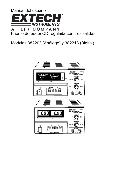
Manual del usuarioFuente de poder CD regulada con tres salidas Modelos 382203 (Análogo) y 382213 (Digital)IntroducciónFelicitaciones por seleccionar la Fuente de poder CD regulado Modelos 382203 (análogo) o 382213 (digital) de Extech. Los modelos 382203 y 382213 son fuentes de poder reguladas de estado sólido y compactos, apropiadas para muchas aplicaciones incluyendo pruebas de banco, servicio de campo, equipo de telecomunicaciones y diversión.Descripción del medidor1. Pantallas LCD Voltaje y Corriente2. LED indicador de estado de límite de corriente3. Interruptor de encendido con LED de estado4. Terminales de salida 5V y 12V fijo5. Terminales de salida alimentación variable6. Perillas de ajuste de voltaje y corriente variableNota: El Modelo 382213 (escalas LCD) se muestra arriba. El Modelo 382203 (mostrado en la portada) usa escala análoga.Operación1. La Fuente de poder debe ser alimentada con voltaje de línea nominal (110V ó 220V) dentro de+ 5%.2. Antes de encender, retire todas las cargas conectadas y fije la perilla de ajuste de voltajetotalmente contrarreloj (salida 0V CD).3. Para operar la fuente de alimentación como fuente de corriente constante, la salida de corrientedebe fijarse entre 10% y 100% del valor nominal (3A). El indicador de limitación de corriente se iluminará al activarse el circuito limitador de corriente.4. Use las perillas para ajuste de corriente y voltaje para fijar las salidas variables de corriente yvoltaje respectivamente. Use las terminales de salida variable para conexiones.5. Para las salidas de 5VCD y 12VCD, use las terminales de salida fija.6. Las pantallas análoga o digital indicaran las salidas reales de corriente y voltaje.7. Mantenga libre de obstrucciones las rejillas de ventilación del medidor (arriba y lados) paraprevenir sobrecalentamiento.Especificaciones382203382213Indicador Análogo doble conescalas Pantalla LCD doble de 3dígitosSalida de voltaje, CD0-30VSalida de corriente, CD0 - 3 amperiosIndicador de límite decorrienteLED de estadoPrecisión ± 7% de la escala total ± 1% de la escala total + 2dígitosOndulación y Ruido< 5mVRegulación de línea< 0,05% + 10mVVoltaje fijo de salida5V / 0,5A (Continuo); 1A (máx.)12V / 0,5A (Continuo); 1A (máx.)Tensión110/220VCA 50/60Hz (conmutable) Dimensiones152 x 142 x 242mm(6 x 5,6 x 9,5") (WxHxD)Peso4,5 kg (10 lbs.)Copyright (c)2012 Extech Instruments Corporation (a FLIR company) Reservados todos los derechos, incluyendo el derecho de reproducción total o parcial en cualquier medi o.。

基于DMA的高速UART串口通信设计与实现DMA (Direct Memory Access) 是一种计算机系统架构的特性,它允许外设在不占用CPU资源的情况下直接访问主存储器。
在UART串口通信中,通过使用DMA可以实现高速的数据传输,提高系统的效率。
首先,我们需要设计一个基于DMA的高速UART串口通信方案。
具体步骤如下:1.确定UART串口通信的参数:包括波特率、数据位、停止位、校验位等。
这些参数需要与通信的设备进行协商和一致。
2.初始化DMA控制器:根据具体的处理器架构和芯片型号,选择适当的DMA控制器并进行初始化。
在初始化过程中,需要设置DMA的工作模式、传输方向(发送或接收)、数据宽度等参数。
3.配置DMA传输通道:DMA控制器通常会提供多个传输通道,我们需要选择一个合适的传输通道并进行配置。
配置过程包括设置数据传输的起始地址、目标地址、传输长度等参数。
4.配置UART串口:根据上述确定的串口参数,配置UART串口的寄存器,使其与DMA控制器进行连接。
确保串口的发送和接收缓冲区与DMA通道进行数据交互。
5.启动DMA传输:设置DMA通道的启动条件,使其开始进行数据传输。
启动条件可以是外部触发,也可以是软件触发。
6.处理DMA中断:在DMA传输完成后,DMA控制器会触发中断信号。
我们需要编写中断处理程序,处理该中断,并进行相应的处理,如数据校验、错误处理等。
通过以上步骤,我们可以实现基于DMA的高速UART串口通信。
以下是一些注意事项和优化建议:1.确保DMA传输通道和UART串口之间的数据传输速度能够匹配,避免出现数据丢失或溢出的情况。
2.针对大规模数据传输,可以使用DMA的循环模式,使得数据的连续传输可以自动循环执行,减少CPU的干预。
3.通过合理设置DMA传输长度和缓冲区大小,可以提高系统的吞吐量和响应速度。
4.在处理DMA中断时,需要注意处理可能发生的错误情况,并进行相应的处理和恢复。


RDA5876编程指南上电配置顺序5875 RF I2C协议5875 Core I2C协议I2C地址配置UART波特率配置UART流控配置PCM接口配置TM配置共用晶体配置32K时钟输入pin配置睡眠握手机制配置蓝牙地址配置PSKEY配置说明寄存器读写说明DUT测试模式进入非调制信号输出调制信号输出上电配置顺序:RDA5875的配置包括RF部分和core部分的配置,分为2种配置方式,一.使用iic来初始化rf部分,配置顺序是:1.芯片上电,拉高LDOON。
2.等待20ms。
3.拉低LDOON4.通过iic配置5875 RF部分。
5.拉高LDOON,等待20ms6.通过iic再次配置5875 RF部分。
7.通过uart 配置5875 pskey rf部分8.通过uart配置5875的core部分。
直接接电池时上电时序图如下:二.使用uart来初始化rf部分,配置顺序是:1.芯片上电,拉高LDOON。
2.等待20ms。
3.通过uart配置5875 RF部分。
4.拉低LDOON,core部分随之复位,复位core部分。
5.拉高LDOON,等待20ms6.通过uart配置5875 RF部分7.通过uart配置5875 pskey rf部分8.通过UART配置5875的core部分。
直接接电池时上电时序图如下:RDA5875的电源输入VBAT可以直接接电池或者接在LDO后,推荐电压范围为3.3v-4v5875 RF 部分I2C 协议:5875 RF 部分的I2C slave 设备地址是0010110。
寄存器地址是8位,数据宽度是16位, 高byte 在前,低byte 在后。
读写寄存器时序如下:Chip addressReg addressChip addressRead Byte 1Read Byte 0注意,read5875 Core部分I2C协议:5875 core部分的I2C slave 设备地址是0010101。

分类: LINUX5.1DMA概述DMA是指外部设备不通过CPU而直接与系统内存交换数据的接口技术。
要把外设的数据读入内存或把内存的数据传送到外设,一般都要通过CPU控制完成,如CPU程序查询或中断方式。
利用中断进行数据传送,可以大大提高CPU的利用率。
但是采用中断传送有它的缺点,对于一个高速I/O设备,以及批量交换数据的情况,只能采用DMA方式,才能解决效率和速度问题。
DMA在外设与内存间直接进行数据交换,而不通过CPU,这样数据传送的速度就取决于存储器和外设的工作速度。
通常系统的总线是由CPU管理的。
在DMA方式时,就希望CPU把这些总线让出来,即CPU连到这些总线上的线处于第三态--高阻状态,而由DMA控制器接管,控制传送的字节数,判断DMA是否结束,以及发出DMA结束信号。
DMA控制器必须有以下功能:1. 能向CPU发出系统保持(HOLD)信号,提出总线接管请求;2. 当CPU发出允许接管信号后,负责对总线的控制,进入DMA方式;3. 能对存储器寻址及能修改地址指针,实现对内存的读写操作;4. 能决定本次DMA传送的字节数,判断DMA传送是否结束5. 发出DMA结束信号,使CPU恢复正常工作状态。
如图是DMA控制器硬件结构示意图。
DMA的可能引脚说明:数据总线:用于传送数据。
地址总线:用于选择存储器地址。
数据传送信号:MEMR为存储器读操作信号,MEMW为存储器写操作信号,IOR为外设读操作信号,IOW为外设写操作信号。
DRQ:DMA请求信号。
是外设向DMA控制器提出要求DMA操作的申请信号。
DACK:DMA响应信号。
是DMA控制器向提出DMA请求的外设表示已收到请求和正进行处理的信号。
HOLD:总线请求信号。
是DMA控制器向CPU要求让出总线的请求信号。
HLDA:总线响应信号,是CPU向DMA控制器表示允许总线请求的应答信号。
5.2DMA工作方式随着大规模集成电路技术的发展,DMA传送已不局限于存储器与外设间的信息交换,而可以扩展为在存储器的两个区域之间,或两种高速的外设之间进行DMA传送,如图所示。

TMS320x2833x,2823x Direct Memory Access (DMA)ModuleReference GuideLiterature Number:SPRUFB8DSeptember2007–Revised April20112SPRUFB8D–September2007–Revised April2011Submit Documentation FeedbackPreface (6)1Introduction (8)2Architecture (10)2.1Block Diagram (10)2.2Peripheral Interrupt Event Trigger Sources (10)2.3DMA Bus (13)3Pipeline Timing and Throughput (13)4CPU Arbitration (15)4.1For the External Memory Interface(XINTF)Zones (15)4.2For All Other Peripherals/Memories (16)5Channel Priority (16)5.1Round-Robin Mode (16)5.2Channel1High Priority Mode (17)6Address Pointer and Transfer Control (17)7ADC Sync Feature (22)8Overrun Detection Feature (24)9Register Descriptions (25)9.1DMA Control Register(DMACTRL)—EALLOW Protected (26)9.2Debug Control Register(DEBUGCTRL)—EALLOW Protected (27)9.3Revision Register(REVISION) (27)9.4Priority Control Register1(PRIORITYCTRL1)—EALLOW Protected (28)9.5Priority Status Register(PRIORITYSTAT) (29)9.6Mode Register(MODE)—EALLOW Protected (30)9.7Control Register(CONTROL)—EALLOW Protected (32)9.8Burst Size Register(BURST_SIZE)—EALLOW Protected (34)9.9BURST_COUNT Register (34)9.10Source Burst Step Register Size(SRC_BURST_STEP)—EALLOW Protected (35)9.11Destination Burst Step Register Size(DST_BURST_STEP)—EALLOW Protected (36)9.12Transfer Size Register(TRANSFER_SIZE)—EALLOW Protected (36)9.13Transfer Count Register(TRANSFER_COUNT) (37)9.14Source Transfer Step Size Register(SRC_TRANSFER_STEP)—EALLOW Protected (37)9.15Destination Transfer Step Size Register(DST_TRANSFER_STEP)—EALLOW Protected (38)9.16Source/Destination Wrap Size Register(SRC/DST_WRAP_SIZE)—EALLOW protected) (38)9.17Source/Destination Wrap Count Register(SCR/DST_WRAP_COUNT) (39)9.18Source/Destination Wrap Step Size Registers(SRC/DST_WRAP_STEP)—EALLOW Protected (39)9.19Shadow Source Begin and Current Address Pointer Registers(SRC_BEG_ADDR_SHADOW/DST_BEG_ADDR_SHADOW)—All EALLOW Protected (40)9.20Active Source Begin and Current Address Pointer Registers(SRC_BEG_ADDR/DST_BEG_ADDR) (40)9.21Shadow Destination Begin and Current Address Pointer Registers(SRC_ADDR_SHADOW/DST_ADDR_SHADOW)—All EALLOW Protected (41)9.22Active Destination Begin and Current Address Pointer Registers(SRC_ADDR/DST_ADDR) (41)Appendix A Revision History (42)3 SPRUFB8D–September2007–Revised April2011Table of Contents Submit Documentation FeedbackList of Figures1DMA Block Diagram (10)2Peripheral Interrupt Trigger Input Diagram (12)34-Stage Pipeline DMA Transfer (13)44-Stage Pipeline With One Read Stall(McBSP as source) (14)5DMA State Diagram (21)6ADC Sync Input Diagram (23)7Overrun Detection Logic (24)8DMA Control Register(DMACTRL) (26)9Debug Control Register(DEBUGCTRL) (27)10Revision Register(REVISION) (27)11Priority Control Register1(PRIORITYCTRL1) (28)12Priority Status Register(PRIORITYSTAT) (29)13Mode Register(MODE) (30)14Control Register(CONTROL) (32)15Burst Size Register(BURST_SIZE) (34)16Burst Count Register(BURST_COUNT) (34)17Source Burst Step Size Register(SRC_BURST_STEP) (35)18Destination Burst Step Register Size(DST_BURST_STEP) (36)19Transfer Size Register(TRANSFER_SIZE) (36)20Transfer Count Register(TRANSFER_COUNT) (37)21Source Transfer Step Size Register(SRC_TRANSFER_STEP) (37)22Destination Transfer Step Size Register(DST_TRANSFER_STEP) (38)23Source/Destination Wrap Size Register(SRC/DST_WRAP_SIZE) (38)24Source/Destination Wrap Count Register(SCR/DST_WRAP_COUNT) (39)25Source/Destination Wrap Step Size Registers(SRC/DST_WRAP_STEP) (39)26Shadow Source Begin and Current Address Pointer Registers(SRC_BEG_ADDR_SHADOW/DST_BEG_ADDR_SHADOW) (40)27Active Source Begin and Current Address Pointer Registers(SRC_BEG_ADDR/DST_BEG_ADDR) (40)28Shadow Destination Begin and Current Address Pointer Registers(SRC_ADDR_SHADOW/DST_ADDR_SHADOW) (41)29Active Destination Begin and Current Address Pointer Registers(SRC_ADDR/DST_ADDR) (41)4List of Figures SPRUFB8D–September2007–Revised April2011Submit Documentation FeedbackList of Tables1Peripheral Interrupt Trigger Source Options (12)2DMA Register Summary (25)3DMA Control Register(DMACTRL)Field Descriptions (26)4Debug Control Register(DEBUGCTRL)Field Descriptions (27)5Revision Register(REVISION)Field Descriptions (27)6Priority Control Register1(PRIORITYCTRL1)Field Descriptions (28)7Priority Status Register(PRIORITYSTAT)Field Descriptions (29)8Mode Register(MODE)Field Descriptions (30)9Control Register(CONTROL)Field Descriptions (32)10Burst Size Register(BURST_SIZE)Field Descriptions (34)11Burst Count Register(BURST_COUNT)Field Descriptions (34)12Source Burst Step Size Register(SRC_BURST_STEP)Field Descriptions (35)13Destination Burst Step Register Size(DST_BURST_STEP)Field Descriptions (36)14Transfer Size Register(TRANSFER_SIZE)Field Descriptions (36)15Transfer Count Register(TRANSFER_COUNT)Field Descriptions (37)16Source Transfer Step Size Register(SRC_TRANSFER_STEP)Field Descriptions (37)17Destination Transfer Step Size Register(DST_TRANSFER_STEP)Field Descriptions (38)18Source/Destination Wrap Size Register(SRC/DST_WRAP_SIZE)Field Descriptions (38)19Source/Destination Wrap Count Register(SCR/DST_WRAP_COUNT)Field Descriptions (39)20Source/Destination Wrap Step Size Registers(SRC/DST_WRAP_STEP)Field Descriptions (39)21Shadow Source Begin and Current Address Pointer Registers(SRC_BEG_ADDR_SHADOW/DST_BEG_ADDR_SHADOW)Field Descriptions (40)22Active Source Begin and Current Address Pointer Registers(SRC_BEG_ADDR/DST_BEG_ADDR)Field Descriptions (40)23Shadow Destination Begin and Current Address Pointer Registers(SRC_ADDR_SHADOW/DST_ADDR_SHADOW)Field Descriptions (41)24Active Destination Begin and Current Address Pointer Registers(SRC_ADDR/DST_ADDR)Field Descriptions (41)25Document Revision History (42)5 SPRUFB8D–September2007–Revised April2011List of Tables Submit Documentation FeedbackPrefaceSPRUFB8D–September2007–Revised April2011Read This First The DMA module described in this reference guide is a Type0DMA.See the TMS320C28xx,28xxx DSP Peripheral Reference Guide(SPRU566)for a list of all devices with a DMA module of the same type,to determine the differences between the types,and for a list of device-specific differences within a type.Notational ConventionsThis document uses the following conventions.•Hexadecimal numbers are shown with the suffix h or with a leading0x.For example,the following number is40hexadecimal(decimal64):40h or0x40.•Registers in this document are shown in figures and described in tables.–Each register figure shows a rectangle divided into fields that represent the fields of the register.Each field is labeled with its bit name,its beginning and ending bit numbers above,and itsread/write properties below.A legend explains the notation used for the properties.–Reserved bits in a register figure designate a bit that is used for future device expansion.Related DocsThe following documents support the2833x and2823x devices and can be downloaded from the Texas Instruments web site:.Data Manual and Errata—SPRS439—TMS320F28335,TMS320F28334,TMS320F28332,TMS320F28235,TMS320F28234, TMS320F28232Digital Signal Controllers(DSCs)Data Manual contains the pinout,signaldescriptions,as well as electrical and timing specifications for the F2833x/2823x devices.SPRZ272—TMS320F28335,F28334,F28332,TMS320F28235,F28234,F28232Digital Signal Controllers(DSCs)Silicon Errata describes the advisories and usage notes for different versions ofsilicon.CPU User's Guides—SPRU430—TMS320C28x CPU and Instruction Set Reference Guide describes the central processing unit(CPU)and the assembly language instructions of the TMS320C28x fixed-point digital signalprocessors(DSPs).It also describes emulation features available on these DSPs.SPRUEO2—TMS320C28x Floating Point Unit and Instruction Set Reference Guide describes the floating-point unit and includes the instructions for the FPU.Peripheral Guides—SPRU566—TMS320x28xx,28xxx DSP Peripheral Reference Guide describes the peripheral reference guides of the28x digital signal processors(DSPs).SPRUFB0—TMS320x2833x,2823x System Control and Interrupts Reference Guide describes the various interrupts and system control features of the2833x and2823x digital signal controllers(DSCs).SPRU812—TMS320x2833x,2823x Analog-to-Digital Converter(ADC)Reference Guide describes how to configure and use the on-chip ADC module,which is a12-bit pipelined ADC.SPRU949—TMS320x2833x,2823x DSC External Interface(XINTF)Reference Guide describes the XINTF,which is a nonmultiplexed asynchronous bus,as it is used on the2833x and2823x devices.6Preface SPRUFB8D–September2007–Revised April2011Submit Documentation Feedback Related Docs SPRU963—TMS320x2833x,2823x Boot ROM Reference Guide describes the purpose and features of the bootloader(factory-programmed boot-loading software)and provides examples of code.It alsodescribes other contents of the device on-chip boot ROM and identifies where all of the informationis located within that memory.SPRUFB7—TMS320x2833x,2823x Multichannel Buffered Serial Port(McBSP)Reference Guide describes the McBSP available on the2833x and2823x devices.The McBSPs allow directinterface between a DSP and other devices in a system.SPRUFB8—TMS320x2833x,2823x Direct Memory Access(DMA)Module Reference Guide describes the DMA on the2833x and2823x devices.SPRUG04—TMS320x2833x,2823x Enhanced Pulse Width Modulator(ePWM)Module Reference Guide describes the main areas of the enhanced pulse width modulator that include digital motorcontrol,switch mode power supply control,UPS(uninterruptible power supplies),and other forms ofpower conversion.SPRUG02—TMS320x2833x,2823x High-Resolution Pulse Width Modulator(HRPWM)Reference Guide describes the operation of the high-resolution extension to the pulse width modulator(HRPWM).SPRUFG4—TMS320x2833x,2823x Enhanced Capture(eCAP)Module Reference Guide describes the enhanced capture module.It includes the module description and registers.SPRUG05—TMS320x2833x,2823x Enhanced Quadrature Encoder Pulse(eQEP)Module Reference Guide describes the eQEP module,which is used for interfacing with a linear or rotaryincremental encoder to get position,direction,and speed information from a rotating machine inhigh-performance motion and position control systems.It includes the module description andregisters.SPRUEU1—TMS320x2833x,2823x Enhanced Controller Area Network(eCAN)Reference Guide describes the eCAN that uses established protocol to communicate serially with other controllers inelectrically noisy environments.SPRUFZ5—TMS320x2833x,2823x Serial Communications Interface(SCI)Reference Guide describes the SCI,which is a two-wire asynchronous serial port,commonly known as a UART.TheSCI modules support digital communications between the CPU and other asynchronous peripheralsthat use the standard non-return-to-zero(NRZ)format.SPRUEU3—TMS320x2833x,2823x DSC Serial Peripheral Interface(SPI)Reference Guide describes the SPI-a high-speed synchronous serial input/output(I/O)port-that allows a serial bitstream of programmed length(one to sixteen bits)to be shifted into and out of the device at aprogrammed bit-transfer rate.SPRUG03—TMS320x2833x,2823x Inter-Integrated Circuit(I2C)Module Reference Guide describes the features and operation of the inter-integrated circuit(I2C)module.Tools Guides—SPRU513—TMS320C28x Assembly Language Tools v5.0.0User's Guide describes the assembly language tools(assembler and other tools used to develop assembly language code),assemblerdirectives,macros,common object file format,and symbolic debugging directives for theTMS320C28x device.SPRU514—TMS320C28x Optimizing C/C++Compiler v5.0.0User's Guide describes the TMS320C28x™C/C++compiler.This compiler accepts ANSI standard C/C++source code andproduces TMS320DSP assembly language source code for the TMS320C28x device.SPRU608—TMS320C28x Instruction Set Simulator Technical Overview describes the simulator, available within the Code Composer Studio for TMS320C2000IDE,that simulates the instructionset of the C28x™core.SPRU625—TMS320C28x DSP/BIOS5.32Application Programming Interface(API)Reference Guide describes development using DSP/BIOS.7 SPRUFB8D–September2007–Revised April2011Read This First Submit Documentation FeedbackReference GuideSPRUFB8D–September2007–Revised April2011 TMS320x2833x Direct Memory Access(DMA)ModuleThe direct memory access(DMA)module provides a hardware method of transferring data between peripherals and/or memory without intervention from the CPU,thereby freeing up bandwidth for other system functions.Additionally,the DMA has the capability to orthogonally rearrange the data as it is transferred as well as“ping-pong”data between buffers.These features are useful for structuring data into blocks for optimal CPU processing.1IntroductionThe strength of a digital signal controller(DSC)is not measured purely in processor speed,but in total system capabilities.As a part of the equation,any time the CPU bandwidth for a given function can be reduced,the greater the system capabilities.Many times applications spend a significant amount of their bandwidth moving data,whether it is from off-chip memory to on-chip memory,or from a peripheral such as an analog-to-digital converter(ADC)to RAM,or even from one peripheral to another.Furthermore,many times this data comes in a format that is not conducive to the optimum processing powers of the CPU.The DMA module described in this reference guide has the ability to free up CPU bandwidth and rearrange the data into a pattern for more streamlined processing.The DMA module is an event-based machine,meaning it requires a peripheral interrupt trigger to start a DMA transfer.Although it can be made into a periodic time-driven machine by configuring a timer as the interrupt trigger source,there is no mechanism within the module itself to start memory transfersperiodically.The interrupt trigger source for each of the six DMA channels can be configured separately and each channel contains its own independent PIE interrupt to let the CPU know when a DMA transfers has either started or completed.Five of the six channels are exactly the same,while Channel1has one additional feature:the ability to be configured at a higher priority than the others.At the heart of the DMA is a state machine and tightly coupled address control logic.It is this address control logic that allows for rearrangement of the block of data during the transfer as well as the process of ping-ponging databetween buffers.Each of these features,along with others will be discussed in detail in this document.DMA Overview:•6channels with independent PIE interrupts•Peripheral interrupt trigger sources–ADC sequencer1and sequencer2–Multichannel Buffered Serial Port A and B(McBSP-A,McBSP-B)transmit and receive–XINT1-7and XINT13–CPU Timers–ePWM1-6ADCSOCA and ADSOCB signals–Software•Data sources/destinations:–L4-L716K x16SARAM–All XINTF zones–ADC memory bus mapped result registers–McBSP-A and McBSP-B transmit and receive buffers–ePWM1-6/HRPWM1-6Peripheral Frame3mapped registers•Word Size:16-bit or32-bit(McBSPs limited to16-bit)•Throughput:4cycles/word(5cycles/word for McBSP reads)8TMS320x2833x Direct Memory Access(DMA)Module SPRUFB8D–September2007–Revised April2011Submit Documentation Feedback Introduction NOTE:The ePWM/HRPWM are not present on all devices and/or revisions.See the TMS320x28xx,28xxx DSP Peripheral Reference Guide(SPRU566)for specifics.9 SPRUFB8D–September2007–Revised April2011TMS320x2833x Direct Memory Access(DMA)Module Submit Documentation FeedbackArchitecture 2Architecture2.1Block DiagramFigure1shows a device level block diagram of the DMA.Figure1.DMA Block DiagramA The ePWM/HRPWM registers must be remapped to PF3(through bit0of the MAPCNF register)before they can beaccessed by the DMA.The ePWM/HRPWM connection to DMA is not present in silicon revision0.2.2Peripheral Interrupt Event Trigger SourcesThe peripheral interrupt event trigger can be independently configured as one of eighteen differentsources for each of the six DMA channels.Included in these sources are8external interrupt signals which can be connected to most of the general-purpose input/output(GPIO)pins on the device.This addssignificant flexibility to the event trigger capabilities.A bit field called PERINTSEL in the MODE register of each channel is used to select that channels interrupt trigger source.An active peripheral interrupt trigger will be latched into the PERINTFLG bit of the CONTROL register,and if the respective interrupt and DMA channel is enabled(see the MODE.CHx[PERINTE]and CONTROL.CHx[RUNSTS]bits),it will be serviced by the DMA channel.Upon receipt of a peripheral interrupt event signal,the DMA will automatically send a clear signal to the interrupt source so that subsequent interrupt events will occur.Regardless of the value of the MODE.CHx[PERINTSEL]bit field,software can always force a trigger by using the CONTROL.CHx[PERINTFRC]bit.Likewise,software can always clear a pending DMA trigger using the CONTROL.CHx[PERINTCLR]bit.10TMS320x2833x Direct Memory Access(DMA)Module SPRUFB8D–September2007–Revised April2011Submit Documentation Feedback Architecture Once a particular interrupt trigger sets a channel’s PERINTFLG bit,the bit stays pending until the priority logic of the state machine starts the burst transfer for that channel.Once the burst transfer starts,the flag is cleared.If a new interrupt trigger is generated while a burst is in progress,the burst will complete before responding to the new interrupt trigger(after proper prioritization).If a third interrupt trigger occurs before the pending interrupt is serviced,an error flag is set in the CONTROL.CHx[OVRFLG]bit.If a peripheral interrupt trigger occurs at the same time as the latched flag is being cleared,the peripheral interrupttrigger has priority and the PERINTFLG will remain set.Figure2shows a diagram of the trigger select circuit.See the MODE.CHx[PERINTSEL]bit fielddescription for the complete list of peripheral interrupt trigger sources.11 SPRUFB8D–September2007–Revised April2011TMS320x2833x Direct Memory Access(DMA)Module Submit Documentation FeedbackNoneSEQ1INT SEQ2INT EPWM5SOCBEPWM6SOCA EPWM6SOCB...Architecture Figure 2.Peripheral Interrupt Trigger Input DiagramTable 1shows the interrupt trigger source options that are available for each channel.Table 1.Peripheral Interrupt Trigger Source OptionsPeripheralInterrupt Trigger Source CPUDMA Software bit (CHx.CONTROL.PERINTFRC)only ADCSequencer 1Interrupt Sequencer 2Interrupt External Interrupts External Interrupt 1External Interrupt 2External Interrupt 3External Interrupt 4External Interrupt 5External Interrupt 6External Interrupt 7External Interrupt 13CPU Timers Timer 0OverflowTimer 1OverflowTimer 2OverflowMcBSP-AMcBSP-A Transmit Buffer Empty McBSP-A Receive Buffer Full McBSP-BMcBSP-B Transmit Buffer Empty McBSP-B Receive Buffer Full ePWM1(1)ADC Start of Conversion A ADC Start of Conversion B ePWM2(1)ADC Start of Conversion AADC Start of Conversion BePWM3(1)ADC Start of Conversion A (1)The ePWM1-6are not present on all devices and/or revisions.Seethe TMS320x28xx,28xxx DSP Peripheral Reference Guide(SPRU566)for specifics.12TMS320x2833x Direct Memory Access (DMA)ModuleSPRUFB8D–September 2007–Revised April 2011Submit Documentation FeedbackSYSCLKAddr bus Data bus Generate address Pipeline Timing and ThroughputTable 1.Peripheral Interrupt Trigger Source Options(continued)PeripheralInterrupt Trigger Source ADC Start of Conversion B ePWM4(1)ADC Start of Conversion A ADC Start of Conversion B ePWM5(1)ADC Start of Conversion A ADC Start of Conversion B ePWM6(1)ADC Start of Conversion AADC Start of Conversion B2.3DMA BusThe DMA bus architecture consists of a 22-bit address bus,a 32-bit data read bus,and a 32-bit data write bus.Memories and register locations connected to the DMA bus are via interfaces that sometimes share resources with the CPU memory or peripheral bus.Arbitration rules are defined in Section 4.The following resources are connected to the DMA bus:•XINTF Zones 0,6&7•L4SARAM•L5SARAM•L6SARAM•L7SARAM•ADC Memory Mapped Result Registers•McBSP-A and McBSP-B Data Receive Registers (DRR2/DRR1)and Data Transmit Registers(DXR2/DXR1)•ePWM1-6/HRPWM1-6Register when mapped to Peripheral Frame 33Pipeline Timing and ThroughputThe DMA consists of a 4-stage pipeline as shown in Figure 3.The one exception to this is when a DMA channel is configured to have one of the McBSPs as its data source.A read of a McBSP DRR register stalls the DMA bus for one cycle during the read portion of the transfer,as shown in Figure 4.Figure 3.4-Stage Pipeline DMA Transfer13SPRUFB8D–September 2007–Revised April 2011TMS320x2833x Direct Memory Access (DMA)Module Submit Documentation FeedbackSYSCLKAddr bus Data bus Generate addressPipeline Timing and Throughput Figure 4.4-Stage Pipeline With One Read Stall (McBSP as source)14TMS320x2833x Direct Memory Access (DMA)Module SPRUFB8D–September 2007–Revised April 2011Submit Documentation Feedback CPU ArbitrationIn addition to the pipeline there are a few other behaviors of the DMA that affect it’s total throughput•A1-cycle delay is added at the beginning of each burst•A1-cycle delay is added when returning from a CH1high priority interrupt•32-bit transfers run at double the speed of a16-bit transfer(i.e.,it takes the same amount of time to transfer a32-bit word as it does a16-bit word)•Collisions with the CPU may add delay slots(see Section4)For example,to transfer12816-bit words from ADC to RAM a channel can be configured to transfer8 bursts of16words/burst.This will give:8bursts*[(4cycles/word*16words/burst)+1]=520cyclesIf instead the channel were configured to transfer the same amount of data32bits at a time(the word size is configured to32bits)the transfer would take:8bursts*[(4cycles/word*8words/burst)+1]=264cycles4CPU ArbitrationTypically,DMA activity is independent of the CPU activity.Under the circumstance where both the DMA and the CPU are attempting to access memory or a peripheral register within the same interfaceconcurrently,an arbitration procedure will occur.The one exception is with the memory mapped(PF0) ADC registers,which do not create a conflict when read by both the CPU and the DMA simultaneously, even if different addresses are accessed.Any combined accesses between the different interfaces,orwhere the CPU access is outside of the interface that the DMA is accessing do not create a conflict.The interfaces which internally contain conflicts are:•XINTF Memory Zones0,6and7•L4RAM•L5RAM•L6RAM•L7RAM•Peripheral Frame3(McBSP-A,McBSP-B,and ePWM1-6/HRPWM1-6)NOTE:The ePWM/HRPWM are not present on all devices and/or revisions.See the TMS320x28xx,28xxx DSP Peripheral Reference Guide(SPRU566)for specifics.4.1For the External Memory Interface(XINTF)Zones•If the CPU and the DMA attempt an access to any of the XINTF zones on the same cycle,the DMA is serviced first,followed by all the pending CPU accesses(in the proper priority order for CPU accesses: write→read→fetch).•If CPU accesses to an XINTF zone are pending or being processed by the XINTF and a DMA access to an XINTF zone is attempted,the DMA access is stalled until all CPU pending accesses arecompleted.For example,if a CPU write and read access is pending and a fetch is in progress,first the fetch is completed,then the CPU write is performed,then the CPU read is performed,and then theDMA access is performed.•There is a1cycle stall if simultaneous write accesses by the CPU and the DMA are attempted.If the DMA or CPU is used to write to the XINTF zones,then the write buffer of the XINTF can help toavoid CPU or DMA stalls.If the CPU or DMA are performing reads from XINTF,then significant stalls can occur.The only concern here is if the DMA is stalled and the DMA misses other higher priority DMAevents such as servicing the ADC which can generate data at a high rate.In such situations,the DMAshould not be used to transfer data on XINTF,if the stalls are too long that there is potential to miss other DMA events.15 SPRUFB8D–September2007–Revised April2011TMS320x2833x Direct Memory Access(DMA)Module Submit Documentation FeedbackChannel Priority The DMA does not support abort mechanisms for DMA reads from XINTF.If the DMA is performing an access to one of the XINTF zones and the DMA access is stalled(XREADY not responding)then the CPU can issue a HARDRESET that would abort the access.HARDRESET behaves like a System Reset on the DMA.Likewise,a HARDRESET needs to be applied to the XINTF hence releasing the peripheral from the struck ready condition.Any data that is write buffered or pending on the XINTF or DMA will be lost.4.2For All Other Peripherals/Memories•If the CPU and the DMA make an access to the same interface in the same cycle,the DMA has priority and the CPU is stalled.•If a CPU access to an interface is in progress and another CPU access to the same interface is pending,for example,the CPU is performing a write operation and a read operation from the CPU ispending,then a DMA access to that same interface has priority over the pending CPU access whenthe current CPU access completes.NOTE:If the CPU is performing a read-modify-write operation and the DMA performs a write to thesame location,the DMA write may be lost if the operation occurs in between the CPU readand the CPU write.For this reason,it is advised not to mix such CPU accesses with DMAaccesses to the same locations.In the case of RAM,a ping-pong scheme can be implemented to avoid the CPU and the DMA accessing the same RAM block concurrently,thus avoiding any stalls or corruption issues.5Channel PriorityTwo priority schemes exist when determining channel priority:Round-robin mode and Channel1high-priority mode.5.1Round-Robin ModeIn this mode,all channels have equal priority and each enabled channel is serviced in round-robin fashion as follows:CH1→CH2→CH3→CH4→CH5→CH6→CH1→CH2→…In the case above,after each channel has transferred a burst of words,the next channel is serviced.You can specify the size of the burst for each channel.Once CH6(or the last enabled channel)has beenserviced,and no other channels are pending,the round-robin state machine enters an idle state.From the idle state,channel1(if enabled)is always serviced first.However,if the DMA is currentlyprocessing another channel x,all other pending channels between x and the end of the round are serviced before CH1.It is in this sense that all the channels are of equal priority.For instance,take an example where CH1,CH4,and CH5are enabled in round-robin mode and CH4is currently being processed.Then CH1and CH5both receive an interrupt trigger from their respective peripherals before CH4completes.CH1and CH5are now both pending.When CH4completes its burst,CH5will be serviced next.Only after CH5completes will CH1be serviced.Upon completion of CH1,if there are no more channels pending,the round-robin state machine will enter an idle state.A more complicated example is shown below:•Assume all channels are enabled,and the DMA is in an idle state,•Initially a trigger occurs on CH1,CH3,and CH5on the same cycle,•When the CH1burst transfer starts,requests from CH3and CH5are pending,•Before completion of the CH1burst,the DMA receives a request from CH2.Now the pending requests are from CH2,CH3,and CH5,•After completing the CH1burst,CH2will be serviced since it is next in the round-robin scheme after CH1.•After the burst from CH2is finished,the CH3burst will be serviced,followed by CH5burst.•Now while the CH5burst is being serviced,the DMA receives a request from CH1,CH3,and CH6.16TMS320x2833x Direct Memory Access(DMA)Module SPRUFB8D–September2007–Revised April2011Submit Documentation Feedback。

提供OVP 和EMI 保护的精密、 低噪声、低偏置电流运算放大器 数据手册ADA4177-1/ADA4177-2/ADA4177-4Rev. DDocument FeedbackInformation furnished by Analog Devices is believed to be accurate and reliable. However, no responsibility is assumed by Analog Devices for its use, nor for any infringements of patents or other rights of third parties that may result from its use. Specifications subject to change without notice. No license is granted by implication or otherwise under any patent or patent rights of Analog Devices. Trademarks andregistered trademarks are the property of their respective owners.One Technology Way, P .O. Box 9106, Norwood, MA 02062-9106, U.S.A.Tel: 781.329.4700 ©2014–2017 Analog Devices, Inc. All rights reserved. Technical Support /cnADI 中文版数据手册是英文版数据手册的译文,敬请谅解翻译中可能存在的语言组织或翻译错误,ADI 不对翻译中存在的差异或由此产生的错误负责。
如需确认任何词语的准确性,请参考ADI 提供的最产品特性低失调电压:60 μV (最大值,25°C ,8引脚和14引脚SOIC ) 低失调电压漂移:1 μV/°C (最大值,8引脚和14引脚SOIC ) 低输入偏置电流:1 nA (最大值,25°C )低电压噪声密度:8 nV/√Hz (典型值,1 kHz )大信号电压增益(AVO):100 dB (最小值,全电源电压和工作温度范围)支持高于或低于供电轨电压32 V 的输入过压保护 集成EMI 滤波器70 dB (1000 MHz 下的典型抑制) 90 dB (2400 MHz 下的典型抑制) 轨到轨输出摆幅低供电电流:每个放大器500 µA (典型值) 宽带宽增益带宽积(A V = 100):3.5 MHz (典型值) 单位增益交越(A V = 1):3.5 MHz (典型值) −3 dB 带宽(A V = 1):6 MHz (典型值) 双电源供电额定电压±5 V 至±15 V ,工作电压±2.5 V 至±18 V 单位增益稳定 无反相长期失调电压漂移(10,000小时):2 µV (典型值) 温度迟滞:2 µV (典型值)应用无线基站控制电路 光纤网络控制电路 仪器仪表传感器和控制元件热电偶、RTD 、应变计、分流测量概述ADA4177-1单通道、ADA4177-2双通道和ADA4177-4四通道放大器具有低失调电压(2 μV 典型值)和低漂移(1 μV/°C 最大值)、低输入偏置电流、低噪声和低功耗(500 μA 典型值)特性。

SAM3U系列7.脉宽调制控制器(PWM)宏单元独立的控制4个通道。
每个通道控制两个互补的输出方波。
输出波形的特性,如:周期、占空比、极性以及死区时间(也称为死区或非重叠时间),可以通过用户接口进行配置。
每个通道可从时钟产生器提供的时钟中选择其中一个来使用。
时钟产生器提供的时钟都是由PWM主控时钟(MCK)分频而来的。
可通过映射到外设总线的寄存器来访问PWM宏单元。
所有的通道都集成了一个双缓存系统,以防止由于修改周期、占空比或是死区时间而产生不期望的输出波形。
可以把多个通道链接起来作为同步通道,这样能够同时更新它们的占空比或死区时间。
对同步通道占空比的更新,可通过外设DMA控制器通道(PDC)来完成,PDC可以提供缓冲传输而不需要处理器的干预。
PWM提供8个独立的比较单元,能够将程序设定的值与同步通道的计数器(通道0的计数器)进行比较。
通过比较可以产生软件中断、在2个独立的事件线上触发脉冲(目的是将ADC的转换分别与灵活的PWM输出进行同步)以及触发PDC传输请求。
为了与它们的计数器同步或异步,PWM的输出可以地被覆盖。
PWM模块提供了故障保护机制,它有4个故障输入,能够检测故障条件以及异步地覆盖PWM的输出。
为了使用安全,一些控制寄存器是写保护的。
845 SAM3U数据手册之中文翻译,由武汉理工大学UP团队友情提供,仅供学习交流之用,欢迎指正,共同修改完善。
37.23737--1.控制器方框图PWMFIxPWMFI037.3引脚描述每个通道使用两个外部I/O 引脚提供互补输出。
表3737--1./O 引脚描述系列46SAM3U 数据手册之中文翻译,由武汉理工大学UP 团队友情提供,仅供学习交流之用,欢迎指正,共同修改完善。
描述类型PWMHx 通道x 的PWM 波形输出高输出PWMLx 通道x 的PWM 波形输出低输出PWMFIxPWM 故障输入x输入SAM3U系列7.7.44.1/O引脚接口的引脚是与PIO引脚复用的,因此程序员必须先对PIO控制器进行编程,将PWM所需的引脚配置成外设功能。


RDA Microelectronics, Inc.RDA5872 编程指南_v1.1RDA5872P 编程指南REV V1.0 V1.1 DATE 2010-11-12 2010-12-02 AUTHER Gibson Gibson CHANGE DESCRIPTION Initial version. Modified base on RDA5872P’s programming guide. Modified power on timing上电配置顺序 5872P RF I2C 协议 5872P Core I2C 协议 I2C 地址配置 UART 波特率配置 UART 流控配置 PCM 接口配置 TM 配置 共用晶体配置 32K 时钟输入 pin 配置 睡眠握手机制配置The information contained herein is the exclusive property of RDA and shall not be distributed, reproduced, or disclosed in whole or in part without prior written permission of RDA. Page 1 of 19RDA Microelectronics, Inc.RDA5872 编程指南_v1.1上电配置顺序:RDA5872P 的配置包括 RF 部分和 core 部分的配置,配置顺序是(LDOON) : 1. 芯片上电,拉高 LDOON。
等待 20ms 2. 通过 UART 配置 5872P PMU 部分,包括 TM 模式选择,VBAT 上电后默认为 001。
3. 拉低 LDOON,core 部分随之复位,复位 core 部分。
4. 拉高 LDOON,内置 ROM 中软件开始 run,软件初始化的时间需要 20ms,这之后 uart 才能通信。
5. 通过 UART 配置 5872P RF 部分。
U ni c o r e C o n f i dINSTALLATION AND OPERATIONUSER MANUALData subject to change without notice.Communications, Inc.Copyright© 2009-2021, Unicore RTK Positioning ModuleAll-constellation All-frequency GPS/BDS/GLONASS/Galileo U M 4B0DisclaimerInformation in this document is subject to change without notice and does not represent a commitment on the part of Unicore Communications, Inc. No part of this manual may be reproduced or transmitted in any form or by any means, electronic or mechanical, including photocopying and recording, for any purpose without the express written permission of a duly authorized representative of Unicore Communications, Inc. The information contained within this manual is believed to be true and correct at the time of publication.© Copyright 2009-2021 Unicore Communications, Inc. All rights RSV.UM4B0 User Manual ForewordThis <User Manual> offers you information in the features of the hardware, the installation, specification and use of UNICORECOMM UM4B0 product.This manual is a generic version. Please refer to the appropriate part of the manual according to your purchased product configuration, concerning CORS, RTK and Heading.Readers it applies toThis <User Manual> is applied to the technicists who know GNSS Receiver to some extent but not to the general readers.Contents1INTRODUCTION (1)1.1O VERVIEW (1)1.2K EY F EATURES (1)1.3T ECHNICAL S PECIFICATIONS (2)1.4I NTERFACES (2)2HARDWARE (3)2.1D IMENSIONS (3)2.2P IN D EFINITION (T OP V IEW) (4)2.3E LECTRICAL S PECIFICATIONS (6)2.4O PERATIONAL C ONDITIONS (7)2.5P HYSICAL S PECIFICATIONS (7)3HARDWARE DESIGN (8)3.1D ESIGN IN C ONSIDERATIONS (8)3.2UM4B0R EFERENCE D ESIGN (9)3.3P INS (10)3.4PCB P ACKAGING (11)3.5R ESET S IGNAL (12)3.6A NTENNA (12)3.7E XTERNAL A NTENNA F EED D ESIGN (12)4INSTALLATION AND CONFIGURATION (14)4.1ESD H ANDLING P RECAUTIONS (14)4.2H ARDWARE I NSTALLATION (14)4.3S TART U P (17)4.4C ONFIGURATION AND O UTPUT (17)4.4.1Operation Procedures (18)5CONFIGURATION COMMANDS (19)5.1RTK R EFERENCE S TATION C ONFIGURATION (20)5.2RTK R OVER C ONFIGURATION (21)5.3M OVING B ASE C ONFIGURATIONS (21)5.4H EADING C ONFIGURATION (21)6ANTENNA DETECTION (22)7FIRMWARE UPGRADE (22)8PRODUCTION REQUIREMENT (24)9PACKAGING (25)1Introduction1.1OverviewUM4B0 is a high precision positioning and heading RTK module developed by Unicore Communications, targeting light robots, UAVs, intelligent vehicles, GIS information collection, etc.By employing a single UC4C0 (432 channel tracking) baseband chip and a single RF chip, using single-sided SMD packaging, UM4B0 has achieved the smallest size(30x40mm) in this industry with high accuracy heading and positioning output. It can simultaneously track BDS B1I/B2I/B3I/B1C/B2a + GPS L1/L2/L5 + GLONASSL1/L2+Galileo E1/E5a/E5b.Figure 1-1 UM4B0 Module1.2Key Features•30*40mm, the smallest multi-system multi-frequency high precision module •Support GPS L1/L2/L5+GLONASS L1/L2+BDS B1I/B2I/B3I/B1C/B2a+Galileo E1/E5a/E5b•Based on 432 channel NebulasII GNSS SoC•20Hz update rate•Instant RTK initialization and long-distance RTK•Enhanced multi-system multi-frequency RTK technology, JamShield adaptive narrow-band anti-interference and U-AutoAlign multi-path mitigation •Support odometer input and external high-performance IMU interface* •SMD packagingUM4B0 User Manual 1.3Technical SpecificationsTable 1-1 Performance SpecificationsTable 1-2 Functional Ports1.4InterfacesFigure 1-2 Block Diagram1.RF PartThe receiver gets filtered and enhanced GNSS signal from the antenna via a coaxial cable. The RF part converts the RF input signals into the IF signal, and converts IF analog signal into digital signals required for NebulasII (UC4C0) digital processing.2.NebulasII SoC (UC4C0)The UM4B0 incorporates the processing from the NebulasII (UC4C0), UNICORECOMM’s new generation high precision GNSS SoC with 55nm low power design, which supports up to 12 digital intermediate frequency or 8 analog intermediate frequency signals and can track 12 navigation signals with 432 channels.3.1PPSUM4B0 outputs 1 PPS with adjustable pulse width and polarity.4.EventUM4B0 provides 1 Event Mark Input with adjustable pulse width and polarity.2Hardware2.1DimensionsUM4B0 User ManualFigure 2-1 Mechanical Dimensions2.2Pin Definition (Top View)Figure 2-2 UM4B0 Pin DiagramTable 2-2 Pin DefinitionUM4B0 User Manual2.3Electrical SpecificationsTable 2-3 Absolute Maximum Ratings2.4Operational ConditionsTable 2-4 Operational ConditionsNOTE: Since the product contains capacitors at the input, inrush current will occur during power-on. Evaluate in the actual environment in order to check the effect of the supply voltage drop due to the inrush current.2.5Physical SpecificationsTable 2-5 Physical Specifications3Hardware Design3.1Design in ConsiderationsTo make UM4B0 work properly, you need to properly connect the following:The module VCC power-on behavior is repeatable, the initial level is lower than0.4V, and the undershoot and ringing should be guaranteed to be within 5% VCC Provide stable power to the VCC pinConnect all the GND pins to groundConnect VBAT pin to a 3.0V power supplyConnect ANT_IN signal to the antenna, and ensure the 50-ohm impedance matchingConnect ANT_PWR to +3.3~5.5 V voltage, then supply +3.3~5.5 V feed to the antenna through ANT_INEnsure COM1 is connected to a PC or an external processor, and users can use this serial port to receive position data. COM1 is also necessary for firmwareupgradesProperly connect the module’s reset pin FRESET_N to ensure complete reset of the module. It will restore the module to the manufacturing configuration.When ANT_NLOD, ANT_FFLG and antenna detection indication signal are connected, the IO without any pull-up/down of the client MCU terminal isrequired at the input.In order to obtain proper performance, special concerns should be paid during the design:Power supply: A table and low ripple power supply is necessary for good performance. Make sure the peak-to-peak voltage ripple does not exceed50mVpp. It is recommended to use a power chip with current output capacity greater than 2A to power the board.-Use LDO to ensure the purity of power supply-Try to place LDO close to the module in layout-Widen the tracks of power circuit or use copper pour surface to transmit current-Avoid walking through any high-power or high inductance devices such as a magnetic coilInterfaces: Ensure that the signals and baud rate of the main equipment match those of the UM4B0 moduleAntenna interface: Make sure the antenna impedance matches, and the cable is short without any kinks, try to avoid all acute anglesTry to avoid designing in any circuits underneath UM4B0This module is a temperature sensitive device, so dramatic changes in temperature will result in reduced performance. Keep it away as far as possible from any high-power high-temperature air and heating devices3.2UM4B0 Reference DesignFigure 3-1 Minimum Reference DesignFigure 3-2 UM4B0 Reference Design 3.3PinsTable 3-1 Pin Notes3.4 PCB PackagingFigure 3-3 UM4B0 recommended PCB Packaging (unit: mil, in brackets: mm)3.5Reset SignalUM4B0 module can’t work properly unless it is correctly reset after power on. To ensure effective reset, the reset pin (RST) and power supply pin (VCC) must meet the following time sequence requirement. To reset UM4B0 during normal operation, please pull RST pin to low level for more than 5ms.Figure 3-4 UM4B0 RST3.6AntennaThe module has the antenna input pin ANT_IN, which provides a +3.3V antenna feed. When an active antenna of +3.3~5V is adopted, please make sure the 50 Ω antenna impedance is matched.Figure 3-5 UM4B0 Active Antenna Connection3.7External Antenna Feed DesignUM4B0 feeds the antenna signals to the required circuits internally, but in order to effectively prevent damage from lightning and surges, circuit protection should be installed externally to protect the module.High voltage and high-power protection chips should be used to feed the antenna from the outside of the module. A gas discharge tube, varistor, TVS tube and other high-power protective devices may also be used in the antenna circuit to effectively improve the prevention against lightning stroke and surge.ANTFigure 3-6 UM4B0 External Antenna Feed Reference CircuitRemarks:a)L1, feed inductor, 68nH RF inductor in 0603 package is recommended;b)C1, decoupling capacitor, it is recommended to connect two capacitors of 100nF/100pFin parallel;c)C2, DC blocking capacitor, recommended 100pF capacitor.4Installation and Configuration4.1ESD Handling PrecautionsUM4B0 Module is an Electrostatic Sensitive Device (ESD) and special precautions when handling are required.Electrostatic discharge may cause damages to the device. All operations mentioned in this chapter should be carried out on an antistatic workbench, wearing an antistatic wrist strap and using a conductive foam pad. If anantistatic workbench is not available, wear an antistatic wrist strap and connect the other end to a metal frame to avoid the effects of static electricity.Hold the edge of the module, not in direct contact with the componentsPlease check carefully whether the module has obviously loose or damaged components.Figure 4-1 Typical Installation of UM4B0Please check the contents of the package carefully after receiving the package of UM4B0.UM4B0 EVK suite (or evaluation board)User manualUPrecise softwareQualified antennaMMCX antenna cablePC or Laptop with serial ports (Win7 or above), with UPrecise installed4.2Hardware InstallationAfter the above preparation, please follow the steps below to install:Step 1: Make sure to take all the anti-static measures, such as wearing an anti-static wrist strap, grounding the workbench;Step 2: Align UM4B0 transfer board positioning holes and pins with EVK, and fix it in the EVK. EVK provides power supply and standard communication interface for the module to communicate with peripheral devices;NOTE: The RF connector of the board is MMCX, and the suitable connecting wire should be selected according to the package. The input signal gain at the antenna interface is optimal between 20 and 36 dB. Please select the appropriate antenna, antenna cable and online LNA accordingly.Figure 4-2 Installation InstructionStep 3: Select the GNSS antenna with appropriate gain, and fix it in a stable, non-block area, using the coaxial radio frequency cable to connect the antenna to UM4B0 EVK;Step 4: Connect the PC to the EVK serial port through direct serial cable;Figure 4-3 Connect the Serial PortStep 5: Connect a 12V adapter to the EVK power input, and switch on to powerthe device;Figure 4-4 Connect the AntennaStep 6: Open the UPrecise software on the PC;Step 7: Control the receiver through UPrecise to send commands or to log data.4.3Start UpThe power supply for UM4B0 is 3.3VDC. Before powering on the device, please connect UM4B0 serial port to the GNSS antenna. The receiver is started and the communication is connected after powering up. Testing tools are provided for module testing.4.4Configuration and OutputUNICORECOMM UPrecise software provides a user-friendly graphical interface to control and display the operation of your receiver. The features of Uprecise include: Logging Control View: Graphic interface for data loggingConsole window for sending command to the receiver (Console View)Displaying the receiver’s output in ASCII-format (ASCII View)Graphic window for displaying Position of satellite, PRN, and Signal/Noise Ratio (Constellation View)Historical and present Trajectory of the receiver (Trajectory View)Position/Velocity/Time of the receiver (PVT View)Apart from the basic functions above, UPrecise offers advanced functions as follows: Selecting and recording the logSending commands to the receiverOperating and configuration of the ASCII viewThe trajectory view for displaying the present point and the past point of the receiverSwitching Views over the tracking windowSwitching between Constellation ViewsResetting the receiverReplaying the GGA logFigure 4-5 UPrecise SoftwareUM4B0 User Manual 4.4.1Operation ProceduresStep 1. Follow 4.2 Installation Guide to connect the power source, antenna to the board, and turn on the EVK switchStep 2. Click file - > connect the serial port, and set the baud rate; the default baud rate of UB4B0M is 115200bpsFigure 4-6 Connect the Serial PortStep 3. Click the receiver settings button to configure the NMEA message output. Itis recommended to configure GPGGA, GPGSV, and other messages.Figure 4-7 NMEA Data OutputStep 4. Click the receiver settings button to configure the NMEA message output, then click send. It is recommended to configure GPGGA, GPGSV, and other messages. Step 5.In the data session window, click “Send all Message” to complete all the NMEA message output (update rate 1Hz). Right click in the data session window to adjust: output log font size, stop / resume log output, or clear log content, etc.Step 6. Use various views of UPrecise to configure or input commands as required.5Configuration CommandsUM4B0 supports abbreviated ASCII format. Simplified ASCII format without check bit is more accessible to user commands. All commands are composed of a log heading and configuration parameters (If parameters are null, there will be only one heading in the command). Header field contains the command name or message headers. UM4B0 is simple to use, and common instructions are shown in the following table:UM4B0 User Manual5.1RTK Reference Station ConfigurationIf the precise coordinates are known, the precise coordinates could be set as in this example:Mode base 40.07898324818 116.23660197714 60.4265 // set lat lon heightrtcm1033 com2 10 // RTCM1033 input from com2rtcm1006 com2 10rtcm1074 com2 1rtcm1084 com2 1rtcm1094 com2 1rtcm1124 com2 1saveconfigIf precise coordinates are unknown:Mode base time 60 1.5 2.0 // 60 seconds position averagertcm1033 com2 10rtcm1006 com2 10rtcm1074 com2 1rtcm1084 com2 1rtcm1094 com2 1rtcm1124 com2 1saveconfig5.2RTK Rover ConfigurationRTK Rover stations (rover station) receive differential correction data sent from reference stations and receive satellite signals to provide an RTK positioning solution and realize RTK high-precision positioning with cm or mm-level accuracy. Common instructions for configuring RTK rover are as follows:gngga 1saveconfig5.3Moving Base ConfigurationsRTK reference station provides precisely known coordinates of a fixed station. Unlike the RTK reference station, moving base station is in motion, at the same time receives the satellite information, and sends it to the rover station receiver (to be determined) directly or after processing. The rover station receiver receives satellite observations as well as information from the moving base station, to make relative positioning and determine the position of the rover station. Commonly used instructions to set the moving base station are as follows:Mode movingbasertcm1006 com2 1rtcm1074 com2 1rtcm1084 com2 1rtcm1094 com2 1rtcm1124 com2 1saveconfig5.4Heading ConfigurationGNSS heading refers to the clockwise angle between true North and the baseline vector constituted by the two GNSS antennas. Commonly used instructions are as follows:Mode headinggphdt com1 1saveconfigUM4B0 User Manual6Antenna Detection1The UM4B0 module offers antenna open/short detection. The corresponding pins are ANT_NLOAD and ANT_FFLG.•The current monitoring chip outputs 2 bit high and low voltage; the software portion sets 2 bit IO of corresponding NII as input pull-up, and then queries the status of 2 bit IO to check the antenna state.•If ANT_PWR malfunctions, the query result is invalid.•If the antenna is not fed by ANT_PWR but by other means, the query result is invalid.7Firmware UpgradeUprecise software is used for the remote update of UM4B0. Please follow the steps below to upgrade the device:Figure 7-1 Update InterfaceClick “…” to browse the firmware update package, and click“Start” to start the firmware upgrading process (uncheck software reset):1 Optional by FirmwareFigure 7-2 Update StepsWaiting for the process to complete 100% (the upgrade time is normally within 5min):Figure 7-3 Update StepsPlease use COM1 only to update firmware.UM4B0 User Manual8Production RequirementRecommended thermal cycle curve is as follows:Figure 8-1 Soldering TemperatureTemperature rising stage∙Rising slope: Max. 3℃/s∙Rising temperature range:50℃-150℃Preheating stage∙Preheating time: 60 – 120 s∙Preheating temperature range: 150 - 180℃Reflux Stage∙Over melting temperature (217℃) time: 40 – 60 s∙Peak temperature: no higher than 245℃Cooling Stage∙Cooling slope: Max. 4℃ / sNotes:In order to prevent fall off during soldering of the modules, please avoid soldering the module in the back of the Board during design, that is, better not to go through soldering cycle twice.The setting of temperature depends on many factors, such as type of Board, solder paste type, solder paste thickness, etc. Please also refer to the relevant IPC standards and indicators for solder paste.Since the lead soldering temperatures are relatively low, if using this soldering method, please give priority to other components on the Board.9PackagingUM4B0 modules are delivered in trays, which is suitable for mainstream SMT equipment. Each box contains 5 trays, so there are 150 UM4B0 modules in the box. Table 9-1 Package Informationw 。