LM723中文简易资料教学文案
- 格式:docx
- 大小:57.63 KB
- 文档页数:2

Copyright © 1988, Texas Instruments Incorporated PRODUCTION DATA information is current as of publication date.PACKAGING INFORMATIONOrderable Device Status(1)PackageType PackageDrawingPins PackageQtyEco Plan(2)Lead/Ball Finish MSL Peak Temp(3)5962-9675101QCA ACTIVE CDIP J141TBD Call TI Level-NC-NC-NC 5962-9675101QDA ACTIVE CFP W141TBD Call TI Level-NC-NC-NC 5962-9675101QDA ACTIVE CFP W141TBD Call TI Level-NC-NC-NC 5962-9675101VCA ACTIVE CDIP J141TBD Call TI Level-NC-NC-NC 5962-9675101VCA ACTIVE CDIP J141TBD Call TI Level-NC-NC-NC 5962-9675101VDA ACTIVE CFP W141TBD Call TI Level-NC-NC-NC 5962-9675101VDA ACTIVE CFP W141TBD Call TI Level-NC-NC-NC SN54LS73AJ ACTIVE CDIP J141TBD Call TI Level-NC-NC-NC SN54LS73AJ ACTIVE CDIP J141TBD Call TI Level-NC-NC-NC SN7473N OBSOLETE PDIP N14TBD Call TI Call TISN7473N OBSOLETE PDIP N14TBD Call TI Call TISN7473N3OBSOLETE PDIP N14TBD Call TI Call TISN7473N3OBSOLETE PDIP N14TBD Call TI Call TISN74LS73AD ACTIVE SOIC D1450Green(RoHS&no Sb/Br)CU NIPDAU Level-1-260C-UNLIMSN74LS73AD ACTIVE SOIC D1450Green(RoHS&no Sb/Br)CU NIPDAU Level-1-260C-UNLIMSN74LS73ADE4ACTIVE SOIC D1450Green(RoHS&no Sb/Br)CU NIPDAU Level-1-260C-UNLIMSN74LS73ADE4ACTIVE SOIC D1450Green(RoHS&no Sb/Br)CU NIPDAU Level-1-260C-UNLIMSN74LS73ADR ACTIVE SOIC D142500Green(RoHS&no Sb/Br)CU NIPDAU Level-1-260C-UNLIMSN74LS73ADR ACTIVE SOIC D142500Green(RoHS&no Sb/Br)CU NIPDAU Level-1-260C-UNLIMSN74LS73ADRE4ACTIVE SOIC D142500Green(RoHS&no Sb/Br)CU NIPDAU Level-1-260C-UNLIMSN74LS73ADRE4ACTIVE SOIC D142500Green(RoHS&no Sb/Br)CU NIPDAU Level-1-260C-UNLIMSN74LS73AN ACTIVE PDIP N1425Pb-Free(RoHS)CU NIPDAU Level-NC-NC-NCSN74LS73AN ACTIVE PDIP N1425Pb-Free(RoHS)CU NIPDAU Level-NC-NC-NCSN74LS73ANE4ACTIVE PDIP N1425Pb-Free(RoHS)CU NIPDAU Level-NC-NC-NCSN74LS73ANE4ACTIVE PDIP N1425Pb-Free(RoHS)CU NIPDAU Level-NC-NC-NC SNJ54LS73AFD OBSOLETE LCCC FK20TBD Call TI Level-NC-NC-NC SNJ54LS73AFD OBSOLETE LCCC FK20TBD Call TI Level-NC-NC-NC SNJ54LS73AJ ACTIVE CDIP J141TBD Call TI Level-NC-NC-NC SNJ54LS73AJ ACTIVE CDIP J141TBD Call TI Level-NC-NC-NC SNJ54LS73AW ACTIVE CFP W141TBD Call TI Level-NC-NC-NC SNJ54LS73AW ACTIVE CFP W141TBD Call TI Level-NC-NC-NC (1)The marketing status values are defined as follows:ACTIVE:Product device recommended for new designs.LIFEBUY:TI has announced that the device will be discontinued,and a lifetime-buy period is in effect.NRND:Not recommended for new designs.Device is in production to support existing customers,but TI does not recommend using this part in a new design.PREVIEW:Device has been announced but is not in production.Samples may or may not be available.OBSOLETE:TI has discontinued the production of the device.(2)Eco Plan-The planned eco-friendly classification:Pb-Free(RoHS)or Green(RoHS&no Sb/Br)-please check /productcontent for the latest availability information and additional product content details.TBD:The Pb-Free/Green conversion plan has not been defined.Pb-Free(RoHS):TI's terms"Lead-Free"or"Pb-Free"mean semiconductor products that are compatible with the current RoHS requirements for all6substances,including the requirement that lead not exceed0.1%by weight in homogeneous materials.Where designed to be soldered at high temperatures,TI Pb-Free products are suitable for use in specified lead-free processes.Green(RoHS&no Sb/Br):TI defines"Green"to mean Pb-Free(RoHS compatible),and free of Bromine(Br)and Antimony(Sb)based flame retardants(Br or Sb do not exceed0.1%by weight in homogeneous material)(3)MSL,Peak Temp.--The Moisture Sensitivity Level rating according to the JEDEC industry standard classifications,and peak solder temperature.Important Information and Disclaimer:The information provided on this page represents TI's knowledge and belief as of the date that it is provided.TI bases its knowledge and belief on information provided by third parties,and makes no representation or warranty as to the accuracy of such information.Efforts are underway to better integrate information from third parties.TI has taken and continues to take reasonable steps to provide representative and accurate information but may not have conducted destructive testing or chemical analysis on incoming materials and chemicals.TI and TI suppliers consider certain information to be proprietary,and thus CAS numbers and other limited information may not be available for release.In no event shall TI's liability arising out of such information exceed the total purchase price of the TI part(s)at issue in this document sold by TI to Customer on an annual basis.IMPORTANT NOTICETexas Instruments Incorporated and its subsidiaries (TI) reserve the right to make corrections, modifications, enhancements, improvements, and other changes to its products and services at any time and to discontinue any product or service without notice. Customers should obtain the latest relevant information before placing orders and should verify that such information is current and complete. All products are sold subject to TI’s terms and conditions of sale supplied at the time of order acknowledgment.TI warrants performance of its hardware products to the specifications applicable at the time of sale in accordance with TI’s standard warranty. T esting and other quality control techniques are used to the extent TI deems necessary to support this warranty. Except where mandated by government requirements, testing of all parameters of each product is not necessarily performed.TI assumes no liability for applications assistance or customer product design. Customers are responsible for their products and applications using TI components. T o minimize the risks associated with customer products and applications, customers should provide adequate design and operating safeguards.TI does not warrant or represent that any license, either express or implied, is granted under any TI patent right, copyright, mask work right, or other TI intellectual property right relating to any combination, machine, or process in which TI products or services are used. Information published by TI regarding third-party products or services does not constitute a license from TI to use such products or services or a warranty or endorsement thereof. Use of such information may require a license from a third party under the patents or other intellectual property of the third party, or a license from TI under the patents or other intellectual property of TI.Reproduction of information in TI data books or data sheets is permissible only if reproduction is without alteration and is accompanied by all associated warranties, conditions, limitations, and notices. Reproduction of this information with alteration is an unfair and deceptive business practice. TI is not responsible or liable for such altered documentation.Resale of TI products or services with statements different from or beyond the parameters stated by TI for that product or service voids all express and any implied warranties for the associated TI product or service and is an unfair and deceptive business practice. TI is not responsible or liable for any such statements. Following are URLs where you can obtain information on other Texas Instruments products and application solutions:Products ApplicationsAmplifiers Audio /audioData Converters Automotive /automotiveDSP Broadband /broadbandInterface Digital Control /digitalcontrolLogic Military /militaryPower Mgmt Optical Networking /opticalnetwork Microcontrollers Security /securityTelephony /telephonyVideo & Imaging /videoWireless /wirelessMailing Address:Texas InstrumentsPost Office Box 655303 Dallas, Texas 75265Copyright 2005, Texas Instruments Incorporated。
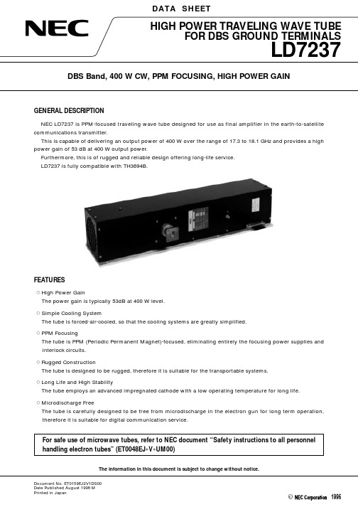
DATA SHEETDocument No. ET0159EJ2V1DS00Date Published August 1998 M Printed in JapanDBS Band, 400 W CW, PPM FOCUSING, HIGH POWER GAINThe information in this document is subject to change without notice.©1996GENERAL DESCRIPTIONNEC LD7237 is PPM-focused traveling wave tube designed for use as final amplifier in the earth-to-satellite communications transmitter.This is capable of delivering an output power of 400 W over the range of 17.3 to 18.1 GHz and provides a high power gain of 53 dB at 400 W output power.Furthermore, this is of rugged and reliable design offering long-life service.LD7237 is fully compatible with TH3694B.FEATURES™High Power GainThe power gain is typically 53dB at 400 W level.™Simple Cooling SystemThe tube is forced-air-cooled, so that the cooling systems are greatly simplified.™PPM FocusingThe tube is PPM (Periodic Permanent Magnet)-focused, eliminating entirely the focusing power supplies and interlock circuits.™Rugged ConstructionThe tube is designed to be rugged, therefore it is suitable for the transportable systems.™Long Life and High StabilityThe tube employs an advanced impregnated cathode with a low operating temperature for long life.™Microdischarge FreeThe tube is carefully designed to be free from microdischarge in the electron gun for long term operation,therefore it is suitable for digital communication service.For safe use of microwave tubes, refer to NEC document “Safety instructions to all personnel handling electron tubes” (ET0048EJ ∗V ∗UM00)2LD7237GENERAL CHARACTERISTICSELECTRICALFrequency ..................................................................................17.3 to 18.1 GHz Output Power ............................................................................400 W Heater Voltage...........................................................................6.3 V Heater Current...........................................................................1.4 AType of Cathode........................................................................Indirectly heated, Impregnated Cathode Warm-up Time ...........................................................300 s MECHANICALDimensions................................................................................See Outline Drawing Weight........................................................................................6.0 kg approx.Focusing ....................................................................................Periodic Permanent Magnet Mounting Position ....................................................................AnyElectrical Connections ..............................................................AMP 861647-8 multi-pin connectorHeater, Heater-Cathode Helix, Anode, Collector and Thermal ProtectionRF ConnectionsInput ...................................................................................Mates with SMA-Female Output ................................................................................Mates with UBR-140 Flange Cooling.......................................................................................Forced AirLD7237ABSOLUTE RATINGS (Note 1, 2 and 3)ELECTRICALMin.Max.Unit Heater Voltage.................................................................. 6.0 6.6VHeater Surge Current......................................................– 4.5AHeater Current..................................................................– 3.0AHeater Warm-up Time.....................................................300–sHelix Voltage....................................................................9.510.75kVHelix Current....................................................................–15mAAnode Voltage..................................................................8.5510.25kVAnode Current..................................................................–0.5mACollector Voltage.............................................................. 4.0 5.5kVCathode Current...............................................................–350mARF Drive Power................................................................–25mWLoad VSWR......................................................................– 1.5MECHANICALMin.Max.Unit Temperature at output Flange........................................–100˚CAir Flow............................................................................195–kg/hrAmbient TemperatureStorage.....................................................................–40+80˚COperation..................................................................–10+50˚C34LD7237TYPICAL OPERATION (Note 2, 3 and 5)UnitFrequency ...............................................................................17.3 to 18.1GHz Output Power .........................................................................400W Heater Voltage (Note 4)........................................................ 6.3V Heater Current........................................................................ 1.4A Helix Voltage...........................................................................10kV Helix Current...........................................................................2mA Anode Voltage........................................................................9.5kV Anode Current........................................................................0.1mA Collector Voltage.................................................................... 4.7kV Cathode Current (290)mAPower Gainat small signal ..................................................................58dB at rated output power .....................................................53dBGain Variation at small signal...............................................2dB/800 MHz Gain Slope at small signal ....................................................0.01dB/MHzAM-PM Conversionat small signal ..................................................................0.5°/dB at rated output power ..................................................... 2.0°/dB 3rd Order Intermodulation(two equal carriers, 40 W total)......................................–32dBc Cooling Air Flow ....................................................................195kg/hr Pressure Drop.........................................................................650PaNote 1:Absolute rating should not be exceeded under continuous or transient conditions.A single absolute rating may be the limitation and simultaneous operation at more than one absolute rating may not be possible.Note 2:The tube body is at ground potential in operation.Note 3:All voltages are refferred to the cathode potential except the heater voltage.Note 4:The optimum operating parameters are shown on a test performance sheet for each tube.Note 5:These characteristics and operating values may be changed as a result of additional information or productimprovement. NEC should be consulted before using this information for equipment design.This data sheet should not be referred to a contractual specification.5LD7237LD7237 OUTLINE (Unit in mm)Pin No.LEAD NAME1HEATER / CATHODE 2HEATER 3COLLECTOR4THERMAL PROTECTION 5OPEN (NO CONNECTION)6HELIX (GROUND)7ANODEPIN ASSIGNMENTNOTE THERMAL PROTECTION : N/C (NormallyClosed) CONTACTLD7237 6LD72377LD7237No part of this document may be copied or reproduced in any form or by any means without the prior written consent of NEC Corporation. NEC Corporation assumes no responsibility for any errors which may appear in this document.NEC Corporation does not assume any liability for infringement of patents. copyrights or other intellectual property rights of third parties by or arising from use of a device described herein or any other liability arising from use of such device. No license, either express, implied or otherwise, is granted under any patents, copyrights or other intellectual property rights of NEC Corporation or others.While NEC Corporation has been making continuous effort to enhance the reliability of its Electronic Conponents, the possibility of defects cannot be eliminated entirely. To minimize risks of damage or injury to persons or property arising from a defect in an NEC Electronic Conponents, customers must incorporate sufficient safety measures in its design, such as redundancy, fire-containment, and anti-failure features.NEC devices are classified into the following three quality grades:“Standard”, “Special”, and “Specific”. The Specific quality grade applies only to devices developed based on a customer designated “quality assurance program” for a specific application. The recommended applications of a device depend on its quality grade, as indicated below. Customers must check the quality grade of each device before using it in a particular application.Standard: Computers, office equipment, communications equipment, test and measurement equipment, audio and visual equipment, home electronic appliances, machine tools, personal electronic equipment and industrial robotsSpecial: Transportation equipment (automobiles, trains, ships, etc.), traffic control systems, anti-disaster systems, anti-crime systems, safety equipment and medical equipment (not specifically designed for life support)Specific: Aircrafis, aerospace equipment, submersible repeaters, nuclear reactor control systems, life support systems or medical equipment for life support, etc.The quality grade of NEC devices is “Standard” unless otherwise specified in NEC's Data Sheets or Data Books.If customers intend to use NEC devices for applications other than those specified for Standard quality grade, they should contact an NEC sales representative in advance.Anti-radioactive design is not implemented in this product.。

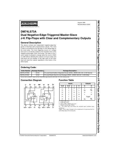
© 2000 Fairchild Semiconductor Corporation DS006372August 1986Revised March 2000DM74LS73A Dual Negative-Edge-Triggered Master-Slave J-K Flip-Flops with Clear and Complementary OutputsDM74LS73ADual Negative-Edge-Triggered Master-SlaveJ-K Flip-Flops with Clear and Complementary OutputsGeneral DescriptionThis device contains two independent negative-edge-trig-gered J-K flip-flops with complementary outputs. The J and K data is processed by the flip-flops on the falling edge of the clock pulse. The clock triggering occurs at a voltage level and is not directly related to the transition time of the negative going edge of the clock pulse. The data on the J and K inputs is allowed to change while the clock is HIGH or LOW without affecting the outputs as long as setup and hold times are not violated. A low logic level on the clear input will reset the outputs regardless of the levels of the other inputs.Ordering Code:Devices also available in T ape and Reel. Specify by appending the suffix letter “X” to the ordering code.Connection Diagram Function TableH = HIGH Logic Level L = LOW Logic LevelX = Either LOW or HIGH Logic Level ↓ = Negative going edge of pulse.Q 0 = The output logic level before the indicated input conditions were established.Toggle = Each output changes to the complement of its previous level on each falling edge of the clock pulse.Order Number Package NumberPackage DescriptionDM74LS73AM M14A 14-Lead Small Outline Integrated Circuit (SOIC), JEDEC MS-120, 0.150 Narrow DM74LS73ANN14A14-Lead Plastic Dual-In-Line Package (PDIP), JEDEC MS-001, 0.300 WideInputsOutputsCLR CLK J K Q Q L X X X L H H ↓L L Q 0Q 0H ↓H L H L H ↓L H L HH ↓H H ToggleHHXXQ 0Q 0 2D M 74L S 73AAbsolute Maximum Ratings (Note 1)Note 1: The “Absolute Maximum Ratings” are those values beyond which the safety of the device cannot be guaranteed. The device should not be operated at these limits. The parametric values defined in the Electrical Characteristics tables are not guaranteed at the absolute maximum ratings.The “Recommended Operating Conditions” table will define the conditions for actual device operation.Recommended Operating ConditionsNote 2: C L = 15 pF, R L = 2 k Ω, T A = 25°C and V CC = 5V.Note 3: C L = 50 pF, R L = 2 k Ω, T A = 25°C and V CC = 5V.Note 4: The symbol (↓) indicates the falling edge of the clock pulse is used for reference.Supply Voltage 7V Input Voltage7VOperating Free Air Temperature Range 0°C to +70°C Storage Temperature Range−65°C to +150°CSymbol ParameterMin Nom Max Units V CC Supply Voltage4.7555.25V V IH HIGH Level Input Voltage 2V V IL LOW Level Input Voltage 0.8V I OH HIGH Level Output Current −0.4mA I OL LOW Level Output Current 8mA f CLK Clock Frequency (Note 2)030MHz f CLK Clock Frequency (Note 3)025MHzt WPulse Width Clock HIGH 20(Note 2)Preset LOW 25nsClear LOW 25t WPulse Width Clock HIGH 25(Note 3)Preset LOW 30ns Clear LOW30t SU Setup Time (Note 2)(Note 4)20↓ns t SU Setup Time (Note 3)(Note 4)25↓ns t H Hold Time (Note 2)(Note 4)0↓ns t H Hold Time (Note 3)(Note 4)5↓ns T AFree Air Operating Temperature70°CDM74LS73AElectrical Characteristicsover recommended operating free air temperature range (unless otherwise noted)Note 5: All typicals are at V CC = 5V, T A = 25°C.Note 6: Not more than one output should be shorted at a time, and the duration should not exceed one second. For devices, with feedback from the outputs,where shorting the outputs to ground may cause the outputs to change logic state, an equivalent test may be performed where V O = 2.125V with the mini-mum and maximum limits reduced by one half from their stated values. This is very useful when using automatic test equipment.Note 7: With all outputs OPEN, I CC is measured with the Q and Q outputs HIGH in turn. At the time of measurement, the clock is grounded.Switching Characteristicsat V CC = 5V and T A = 25°CSymbol ParameterConditionsMinTyp Max Units (Note 5)V I Input Clamp Voltage V CC = Min, I I = −18 mA −1.5V V OH HIGH Level V CC = Min, I OH = Max 2.73.4VOutput Voltage V IL = Max, V IH = Min V OLLOW Level V CC = Min, I OL = Max0.350.5Output VoltageV IL = Max, V IH = Min VI OL = 4 mA, V CC = Min 0.250.4I IInput Current @ Max V CC = Max J, K 0.1Input VoltageV I = 7V Clear 0.3mAClock 0.4I IHHIGH Level V CC = Max J, K 20Input CurrentV I = 2.7VClear 60µA Clock80I ILLOW Level V CC = Max J, K −0.4Input CurrentV I = 0.4VClear −0.8mA Clock−0.8I OS Short Circuit Output Current V CC = Max (Note 6)−20−100mA I CCSupply CurrentV CC = Max (Note 7)46mA From (Input)R L = 2 k ΩSymbol ParameterTo (Output)C L = 15 pF C L = 50 pF UnitsMinMaxMinMaxf MAX Maximum Clock Frequency 3025MHz t PHL Propagation Delay Time Clear 2028ns HIGH-to-LOW Level Output to Q t PLH Propagation Delay Time Clear 2024ns LOW-to-HIGH Level Output to Q t PLH Propagation Delay Time Clock to 2024ns LOW-to-HIGH Level Output Q or Q t PHLPropagation Delay Time Clock to 2028ns HIGH-to-LOW Level OutputQ or Q 4D M 74L S 73APhysical Dimensionsinches (millimeters) unless otherwise noted14-Lead Small Outline Integrated Circuit (SOIC), JEDEC MS-120, 0.150 NarrowPackage Number M14A5DM74LS73A Dual Negative-Edge-Triggered Master-Slave J-K Flip-Flops with Clear and Complementary OutputsPhysical Dimensions inches (millimeters) unless otherwise noted (Continued)14-Lead Plastic Dual-In-Line Package (PDIP), JEDEC MS-001, 0.300 WidePackage Number N14AFairchild does not assume any responsibility for use of any circuitry described, no circuit patent licenses are implied and Fairchild reserves the right at any time without notice to change said circuitry and specifications.LIFE SUPPORT POLICYFAIRCHILD’S PRODUCTS ARE NOT AUTHORIZED FOR USE AS CRITICAL COMPONENTS IN LIFE SUPPORT DEVICES OR SYSTEMS WITHOUT THE EXPRESS WRITTEN APPROVAL OF THE PRESIDENT OF FAIRCHILD SEMICONDUCTOR CORPORATION. As used herein:1.Life support devices or systems are devices or systems which, (a) are intended for surgical implant into the body, or (b) support or sustain life, and (c) whose failure to perform when properly used in accordance with instructions for use provided in the labeling, can be rea-sonably expected to result in a significant injury to the user.2. A critical component in any component of a life support device or system whose failure to perform can be rea-sonably expected to cause the failure of the life support device or system, or to affect its safety or effectiveness.。
OverviewThe LC723700 Series are large-capacity ETR microcontrollers that achieve an instruction execution time of 1.33 µs and provide up to 64 KB of ROM and up to 2 KB of RAM. They include an on-chip high-performance PLL circuit that features an added high-speed lock circuit and can control the C/N characteristics of a local oscillator. They also provide a rich set of on-chip interface circuits, including a 3-channel serial I/O port, and an 8-input 8-bit A/D converter.Functions•ROM—Up to 32K steps (32,767 ×16 bits)—The subroutine area holds 4 K steps (4,096 ×16 bits)•RAM—Up to 4 K ×4 bits (In banks 00 through 3F)LC723732 – ROM: 32 KB, RAM 1 KB LC723740 – ROM: 40 KB, RAM 2 KB LC723748 – ROM: 48 KB, RAM 2 KB LC723756 – ROM: 56 KB, RAM 2 KB LC723764 – ROM: 64 KB, RAM 2 KB •Stack—32 levels •Serial I/O—Three channels. These circuits can support both 2-wire and 3-wire 8-bit communication techniques,and can be switched between MSB first and LSB first operation.—One of six internally generated serial transfer clock rates can be selected: 12.5, 37.5, 187.5, 281.25, 375,and 450 kHz.•External interrupts—Seven interrupt inputs (pins INT0 through INT5, and the HOLD pin)These interrupts can be set to switch between rising and falling edges, although the HOLD pin only supports falling edge detection.•Internal interrupts—Seven interrupts; four internal timer interrupts, and three serial I/O interrupts.•Interrupt nesting levels —16 levels—Interrupt are prioritized in hardware as follows:HOLD pin > INT0 pin > INT1 pin > INT2 pin >INT3 pin > INT4 pin > INT5 pin > S-I/O0 > S-I/O1> S-I/O2 > internal TMR0 > internal TMR1 >internal TMR2 > internal TMR3•A/D converter—8-bit resolution and 8 inputs •General-purpose ports —Input ports: 12—Output ports : 4—I/O ports: 62 (These pins can be switched between input and output in 1-bit units.)•PLL block—Includes a sub-charge pump for high-speed locking.—Supports dead zone control.—Built-in unlock detection circuit.—Twelve reference frequencies: 1, 3, 3.125, 5, 6.25, 9,10, 12.5, 25, 30, 50, and 100 kHz.—A second PLL circuit is also included for use in AM up conversion.•Universal counter—This 20-bit counter can be used for either frequency or period measurement and supports four measurement (calculation) periods: 1, 4, 8, and 32 ms.•Timers—Two fixed timers and two programmable timers (8-bit counters)TMR0: Supports four periods: 10 µs, 100 µs, 1 ms,and 5 msTMR1: Supports four periods: 10 µs, 100 µs, 1 ms,and 10 msTMR2 and TMR3: Programmable 8-bit counters.Input clocks with 10 µs, 100 µs, and 1 ms periods are provided.—One 125-ms timer flip-flop provided.•Beep circuit—Provides 12 fixed beep tones: 0.5, 1, 2, 2.08, 2.2,2.5, 3.33, 3.75, 4.17, and 7.03 kHz.—Programmable 8-bit beep tone generator. Reference clocks with frequencies of 5 kHz, 15 kHz, and 50kHz are provided.•Reset—Built-in voltage detection reset circuit —External reset pinCMOS ICSANYO Electric Co.,Ltd. Semiconductor Bussiness HeadquartersTOKYO OFFICE Tokyo Bldg., 1-10, 1 Chome, Ueno, Taito-ku, TOKYO, 110-8534 JAPANOrdering number : EN5931•Cycle time—1.33 µs (All instructions are one word.)•Halt mode—The microcontroller operating clock is stopped in halt mode.There are four conditions that can clear halt mode: an interrupt request, a timer flip-flop overflow, a PA port input, or a HOLD pin input.•Operating supply voltage—4.5 to 5.5 V (Microcontroller block only: 3.5 to 5.5 V)•Package—QIP100E•OTP version—LC72P3700•Development tools—Emulator :RE32N—Evaluation chip: LC72EV3700—Evaluation chip board: EB-72EV3700Package Dimensions unit: mm3151-QFP100ELC723732/40/48/56/64SANYO: QFP100EPin AssignmentBlock DiagramParameterSymbol ConditionsRatings Unit Maximum supply voltage V DD max –0.3 to +6.5V Input voltage V IN 1PC-PORT–0.3 to +15V V IN 2All input pins other than V IN 1–0.3 to V DD + 0.3V Output voltageV OUT 1PC, PJ-PORT–0.3 to +15V V OUT 2All output pins other than V OUT 1–0.3 to V DD + 0.3V I OUT 1PC, PJ-PORT0 to +5mA Output currentI OUT 2PB, PD, PE, PF, PG, PK, PL, PM, PN, PO, PP, PQ, PR, 0 to +3mA PS, PT, PT-PORT, EO1, EO2, EO3, SUBPD Allowable power dissipation Pd max Ta = –40 to +85°C400mW Operating temperature Topg –40 to +85°C Storage temperatureTstg–45 to +125°CSpecificationsElectrical CharacteristicsAbsolute Maximum Ratings at Ta = 25°C, V SS = 0 VParameterSymbol ConditionsRatingsUnit min typ max V DD 1CPU and PLL operating 4.5 5.05.5V Supply voltageV DD 2CPU operating 3.5 5.5V V DD 3Memory retention1.3 5.5V PB, PC, PH, PI, PL, PM, PN, PO, PP, PQ, PR, V IH 1PS, PT-PORT, HCTR, LCTR, E03, SUBPD 0.7 V DD V DD V(with the I/O ports set to input mode.)Input high-level voltageV IH 2PD, PE, PF, PG, PK-PORT, LCTR,0.8 V DDV DD V (in period measurement mode), HOLD, RESET V IH 3SNS 2.5V DD V V IH 4PA-PORT0.6 V DDV DD V PB, PC, PH, PI, PL, PM, PN, PO, PP, PQ, PR, V IL 1PS, PT-PORT, HCTR, LCTR, E03, SUBPD 00.3 V DD V(with the I/O ports set to input mode.)Input low-level voltageV IL 2PA, PD, PE, PF, PG, PK-PORT, LCTR 00.2 V DDV (in period measurement mode), RESET V IL 3SNS 0 1.3V V IL 4HOLD 00.4 V DDV f IN 1XIN4.0 4.55.0MHz f IN 2FMIN V IN 2, V DD 110150MHz f IN 3FMIN V IN 3, V DD 110130MHz f IN 4AMIN(H) V IN 3, V DD 1 2.040MHz Input frequencyf IN 5AMIN(L) V IN 3, V DD 10.510MHz f IN 6HCTR V IN 3, V DD 10.412MHz f IN 7LCTR V IN 3, V DD 1100500kHz f IN 8LCTR(period measurement)120 ×103Hz V IH 2, V IL 2, V DD 1V IN 1XIN 0.5 1.5Vrms Input amplitude V IN 2FMIN0.07 1.5Vrms V IN 3FMIN, AMIN, HCTR, LCTR 0.04 1.5Vrms Input voltage rangeV IN 4ADI0 to ADI7V DDVAllowable Operating Ranges at Ta = –40 to +85°C, V DD = 3.5 to 5.5 VParameterSymbol ConditionsRatingsUnit min typ maxI IH 1XIN: V I = V DD = 5.0 V2.0 5.015µA I IH 2FMIN, AMIN, HCTR, LCTR: V I = V DD = 5.0 V 4.01030µAPA, PB, PC, PD, PE, PF, PG, PH, PI, PK, PL, PM, PN, PO, PP, PQ, PR, PS, PT-PORT, SNS, HOLD, RESET, HCTR, LCTR, E03, Input high-level currentI IH 3SUBPD: V I = V DD = 5.0 V3.0µA(With the port PA pull-down resistors disabled, and PB, PC, PD, PE, PF, PG, PK, PL, PM, PN, PP, PO, PQ, PR, PS, and PT ports set to input mode.)I IH 4Port PA (pull-down resistors enabled): 50µA V I = V DD = 5.0 V I IL 1XIN: V I = V SS2.0 5.015µA I IL 2FMIN, AMIN, HCTR, LCTR: V I = V SS4.01030µAPA, PB, PC, PD, PE, PF, PG, PH, PI, PK, PL, PM, PN, PO, PP, PQ, PR, PS, PT-PORT, Input low-level currentSNS, HOLD, RESET, HCTR, LCTR, E03, I IL 3SUBPD: V I = V SS3.0µA(With the port PA pull-down resistors disabled, and PB, PC, PD, PE, PF, PG, PK, PL, PM, PN, PP, PO, PQ, PR, PS, and PT ports set to input mode.)Input floating voltage V IF Port PA (pull-down resistors enabled)0.05 V DDV HysteresisV H PD, PE, PF, PG, PK-PORT, RESET,0.1 V DD 0.2 V DDV LCTR(in period measurement mode)V OH 1PB, PD, PE, PF, PG, PK, PL, PM, PN, PO, V DD – 1.0V Output high-level voltagePP, PQ, PR, PS, PT-PORT: I O = –1 mA V OH 2EO1, EO2, EO3, SUBPD: I O = –500 µA V DD – 1.0V V OH 3XOUT: I O = –200 µAV DD – 1.0V V OL 1PB, PD, PE, PF, PG, PK, PL, PM, PN, PO, 1.0V PP, PQ, PR, PS, PT-PORT: I O = 1 mA Output low-level voltageV OL 2E01, E02, E03, SUBPD: I O = 500 µA 1.0V V OL 3XOUT: I O = 200 µA 1.5V V OL 4PC, PJ-PORT: I O = 5 mA2.0V I OFF 1PB, PD, PE, PF, PG, PK, PL, PM, PN, PO, –3.0 3.0µA Output off leakage currentPP, PQ, PR, PS, PT-PORT I OFF 2E01, E02, E03, SUBPD –100100nA I OFF 3PC, PJ-PORT –5.0 5.0µA A/D conversion error ADI0 to ADI7 V DD 1–1.5 1.5LSB Rejected pulse widthP REJ SNS50µsec Power down detection voltage V DET 2.6 3.0 3.4V R PD 1Port PA (pull-down resistors enabled): 75100200k ΩPull-down resistanceV DD = 5 V R PD 2TEST1, TEST210k ΩI DD 1During normal operation (PLL operating)2030mAV DD 1, f IN 2 = 130 MHz Ta = 25°CHalt mode (CPU operation stopped, crystal I DD 2oscillator operating) (See figure 1.)0.45mACurrent drainV DD 2, Ta = 25°C *I DD 3Backup mode (crystal oscillator stopped)5µA (See figure 2.) V DD = 5.5 V, Ta = 25°C I DD 4Backup mode (crystal oscillator stopped)1µA(See figure 2.) V DD = 2.5 V, Ta = 25°C Electrical Characteristics in the allowable operating rangesNote *: Twenty instruction steps are executed every millisecond. The PLL, universal counter, and other functions are stopped.Test CircuitsNote: Ports PB through PG, and PJ through PT are all left open.However, ports PB through PG, PK through PT, EO3, and SUBPD are left open in output mode.Note: Ports PA through PT are all left open.Figure 1 IDD2 in Halt ModeFigure 2 IDD3 and IDD4 in Backup ModePin DescriptionsPin No.SymbolI/OFunctionEquivalent circuitDedicated input ports.These ports are designed with a low threshold voltage.The pull-down resistors for all four pins are set up together with an IOS1 instruction.The pull-down resistors cannot be set individually.Input is disabled in backup mode.32313029PA0PA1PA2PA3I General-purpose I/O portsThe mode (input or output) is set using the IOS2 instruction.Input is disabled and the pins go to the high-impedance state in backup mode.These ports are set up as general-purpose input ports after a power on reset.28272625PB0PB1PB2PB3I/OGeneral-purpose I/O ports (high-voltage input and output)The mode (input or output) is set using the IOS2 instruction.External pull-up resistors are required since the output circuits are open drain circuits.Input is disabled and the pins go to the high-impedance state in backup mode.These ports are set up as general-purpose input ports after a power on reset.24232221PC0PC1PC2PC3I/OGeneral-purpose I/O and external interrupt shared function ports The input formats are Schmitt inputs.The external interrupt function is enabled when the external interrupt enable flag is set.•When used as general-purpose I/O ports:The mode (input or output) is set in 1-bit units using the IOS2 instruction.•When used as external interrupt pins:The external interrupt functions are enabled by setting the corresponding external interrupt enable flag (INT4EN or INT5EN). Here, the pins must be set to input mode in advance.Input is disabled and the pins go to the high-impedance state in backup mode.These ports are set up as general-purpose input ports after a power on reset.20191817PD0/INT4PD1/INT5PD2PD3I/OContinued on next page.Pin No.SymbolI/OFunctionEquivalent circuitGeneral-purpose I/O ports with shared functions as serial I/O portsThe input formats are Schmitt inputs. The PE1/SCK2 and PE2/SO2 pins can be switched to function as open drain outputs.The IOS1 instruction is used to switch between the general-purpose I/O port and serial I/O port functions.•When used as general-purpose I/O ports:The pins are set to the general-purpose I/O port function using the IOS1instruction.The mode (input or output) is set in 1-bit units using the IOS1 instruction.•When used as serial I/O ports:The pins are set to the serial I/O port function using the IOS1 instruction.[Pin states when set to the serial I/O port function]PE0, PF0, PG0 ... General-purpose I/O PE1, PF1, PG1 ... SCK input or output PE2, PF2, PG2 ... SO output PE3, PF3, PG3 ... SI inputThe PE1/SCK2 and PE2/SO2 pins can be switched to function as open drain outputs with the IOS2 instruction. When using this circuit type, the external pull-up resistors must be connected to the same power supply as that used by the IC.Input is disabled and the pins go to the high-impedance state in backup mode.These ports are set up as general-purpose input ports after a power on reset.1615141312111098765PE0PE1/SCK2PE2/S02PE3/SI2PF0PF1/SCK1PF2/S01PF3/SI1PG0PG1/SCK0PG2/S00PG3/SI0I/OConnections for a 4.5-MHz crystal oscillator element1100XIN XOUTI OMain charge pump outputsThese pins output a high level when the frequency of the local oscillator divided by n is higher than that of the reference frequency, and they output a low level when that frequency is lower. They go to the high-impedance state when the frequencies match.These pins go to the high-impedance state in backup mode, after a power on reset,and in the PLL stopped state.9897E01E02OPower supply connectionsThe V DD PORT and V SS PORT pins mainly supply power for the peripheral I/O blocks and the regulator.The V DD PLL and V SS PLL pins mainly for the PLL circuits.The V SS CPU pin is mainly used by the CPU block.The V SS ADC pin is mainly used by the A/D converter block.Since all the V DD and V SS pins are independent, all must be connected to the same power supply.39934408196V DD PORT V DD PLL V SS CPU V SS PORT V SS ADC V SS PLL —Internal low voltage outputConnect a bypass capacitor to this pin.3V REGO FM VCO (local oscillator) inputThis pin is selected with CW1 in the PLL instruction.The signal input to this pin must be capacitor coupled.Input is disabled in backup mode, after a power on reset, and in the PLL stopped state.95FM IN IAM VCO (local oscillator) inputThis pin is selected and the band set with CW1 (b1, b0) in the PLL instruction.The signal input to this pin must be capacitor coupled.Input is disabled in backup mode, after a power on reset, and in the PLL stopped state.94AM IN Ib1b0Band 10 2 to 40 MHz (SW)110.5 to 10 MHz (MW, LW)Continued on next page.Pin No.SymbolI/OFunctionEquivalent circuitSub-charge pump output and general-purpose input shared function portThe IOS2 instruction is used for switching between the sub-charge pump output and general-purpose input functions.•When used as the sub-charge pump output:The sub-charge pump output function is set up with the IOS2 instruction.A high-speed locking circuit can be formed by using this pin in conjunction with the main charge pump.The sub-charge pump is controlled using the DZC instruction.•When used as a general-purpose input:The general-purpose input function is set up with the IOS2 instruction.Data is read from the port using the INR instruction.This pin goes to the high-impedance state in backup mode, after a power on reset,and in the PLL stopped state.92SUBPDI/OSecond PLL charge pump output and general-purpose input shared function port The IOS2 instruction is used for switching between the second PLL charge pump output and general-purpose input functions.•When used as a charge pump output:The charge pump output function is set up with the IOS2 instruction.This pin outputs a low level when the frequency of the local oscillator divided by n is higher than that of the reference frequency, and it outputs a high level when that frequency is lower. It goes to the high-impedance state when the frequencies match. (Note that the logic of this pin is inverted from that of the EO1 and EO2pins.)•When used as a general-purpose input:The general-purpose input function is set up with the IOS2 instruction.Data is read from the port using the INR instruction.This pin goes to the high-impedance state in backup mode, after a power on reset,and in the PLL stopped state.91E03I/OUniversal counter and general-purpose input shared function input portThe IOS1 instruction is used for switching between the universal counter and general-purpose input functions.•When used for frequency measurement:The universal counter function is set up with the IOS1 instruction.The counter is controlled using the UCS and UCC instructions.Since this pin functions as an AC amplifier in this mode, the input signal must be input with capacitor coupling.•When used as a general-purpose input pin:The general-purpose input function is set up with the IOS1 instruction.Data is read from the port using the INR (b0) instruction.Input is disabled in backup mode. (The input pin will be pulled down.) The universal counter function is selected after a power on reset.90HCTR IUniversal counter (frequency or period measurement) and general-purpose input shared function input portThe IOS1 instruction is used for switching between the universal counter and general-purpose input functions.•When used for frequency measurement:The universal counter function is set up with the IOS1 instruction.Set up LCTR frequency measurement mode with the UCS instruction, and control operation with the UCC instruction. Since this pin functions as an AC amplifier in this mode, the input signal must be input with capacitor coupling.•When used for period measurement:The universal counter function is set up with the IOS1 instruction.Set up LCTR frequency measurement mode with the UCS instruction, and control operation with the UCC instruction. Since the bias feedback resistor is disconnected in this mode, the input signal must be input with DC coupling.•When used as a general-purpose input pin:The general-purpose input port function is set up with the IOS1 instruction.Data is read from the port using the INR (b1) instruction.Input is disabled in backup mode. (The input pin will be pulled down.)The universal counter function (HCTR frequency measurement mode) is selected after a power on reset.89LCTR Ib3b2Operation00High impedance01Only operates when the PLL is unlocked (450 kHz)10Only operates when the PLL is unlocked (900 kHz)11Normal operationPin No.SymbolI/OFunctionEquivalent circuitVoltage sense and general-purpose input shared function port This input circuit is designed with a low input threshold voltage.•When used as a voltage sense input:This pin is used to test for power failures on the return from backup mode.Application can test this condition using the internal SNS flip-flop. The SNS flip-flop can be tested with the TST instruction.(This usage requires external components (capacitors and resistors). See the sample application circuit in the user's manual.)•When used as a general-purpose input port:When used as a general-purpose input port the pin state can be tested with the TST instruction.Unlike the other input ports, input to this pin is not disabled in backup mode and after a power on reset. As a result, through currents must be taken into account when designing applications that use this pin as a general-purpose input.88SNS IPower supply monitor (with interrupt function)This pin is designed with a high input threshold voltage.This pin is normally connected to the ACC line and used for power off detection.When a power off state is detected, the HOLDON flag and the hold interrupt request flag will be set. To enter backup mode, execute a CKSTP instruction when the HOLD pin is low. Set this pin high to clear backup mode.87HOLD ISystem reset pinWhen the CPU is operating or in halt mode, the system is reset when this pin is held low for at least one machine cycle. Execution starts with the PC pointing to location 0. At this time the SNS flip-flop is set. A low level must be applied for at least 50 ms when power is first applied.86RESET IGeneral-purpose input and A/D converter input shared function portsThe IOS1 instruction is used to switch between the general-purpose input and the A/D converter input functions.•When used as a general-purpose input ports:The general-purpose input port function is set up with the IOS1 instruction. (In bit units)•When used as A/D converter input pins:The A/D converter input port function is set up with the IOS1 instruction. (In bit units)The pin whose voltage is to be converted is specified with the IOS1 instruction, and the conversion is started with the UCC instruction.Note: Since input is disabled for ports specified for the ADI function, executing aninput instruction for such a port will always return a low level.Input is disabled in backup mode.These ports are set up as general-purpose input ports after a power on reset.8584838281807978PH0/ADI0PH1/ADI1PH2/ADI2PH3/ADI3PI0/ADI4PI1/ADI5PI2/ADI6PI3/ADI7IGeneral-purpose output portsSince these are open-drain output circuits, external pull-up resistors are required.The internal transistors are turned off (resulting in a high-level output) in backup mode and after a power on reset.76757473PJ0PJ1PJ2PJ3OGeneral-purpose I/O and external interrupt shared function ports The input formats are Schmitt inputs.The external interrupt function is enabled when the external interrupt enable flag is set.• When used as general-purpose I/O ports:The mode (input or output) is set in 1-bit units using the IOS1 instruction.• When used as external interrupt pins:The external interrupt functions are enabled by setting the corresponding external interrupt enable flag (INT0EN through INT3EN). Here, the pins must be set to input mode in advance.Input is disabled and the pins go to the high-impedance state in backup mode.These ports are set up as general-purpose input ports after a power on reset.72717069PK0/INT0PK1/INT1PK2/INT2PK3/INT3I/OContinued on next page.Continued from preceding page.Pin No.Symbol I/OFunctionEquivalent circuitGeneral-purpose I/O portsThe mode is switched between input and output with the IOS instruction.Input is disabled and the pins go to the high-impedance state in backup mode.These ports are set up as general-purpose input ports after a power on reset.68 to 61PL0 to 3PN0 to 3I/OGeneral-purpose I/O port and beep tone output shared function portsThe IOS2 instruction is used to switch between the general-purpose I/O port and the beep tone output functions.•When used as a general-purpose input ports:The general-purpose I/O port function is set up with the IOS2 instruction.(Pins PN1 through PN3 are general-purpose I/O pins.)•When used as the beep tone output pin:The beep tone output function is set up with the IOS2 instruction.The frequency is set with the BEEP instruction.When this pin is used as the beep tone output pin, executing an output instruction for this pin only sets the internal latch and has no influence on the output.Input is disabled and the pins go to the high-impedance state in backup mode.These ports are set up as general-purpose input ports after a power on reset.60595857PN0/BEEP PN1PN2PN3I/OGeneral-purpose I/O portsThe mode is switched between input and output with the IOS instruction.Input is disabled and the pins go to the high-impedance state in backup mode.These ports are set up as general-purpose input ports after a power on reset.56 to 49P00 to 3PP0 to 3I/OGeneral-purpose I/O portsThe mode is switched between input and output with the IOS instruction, and data is input with the INR instruction and output with the OUTR instruction.The SPB, RPB, TPT, and TPF instruction cannot be used with these ports.Input is disabled and the pins go to the high-impedance state in backup mode.These ports are set up as general-purpose input ports after a power on reset.48 to 4138 to 33PQ0 to 3PR0 to 3PS0 to 3PT0 to 1I/OIC test pinsThese pins must be tied to ground.992TEST1TEST2LC723700 Instruction Set Abbreviations ADDR:Program memory address b:Borrow c:CarryDH:Data memory address High (Row address) [2 bits]DL:Data memory address Low(Column address) [4 bits]I:Immediate data [4 bits]M:Data memory address N:Bit position [4 bits]M ADR :M specified by address registerROM ADR :Program memory data specified by address register P1n, P2n:Port number [4 bits]PW1n, PW2n:Port control word number [4 bits]PEn:Peripheral register number [4 bits]SR:ADR/DTRADR:Address register DTR:Data registerr:General register (One of the address from 00H to 0FH of BANK0)SWR:Status write register SRR:Status read register( ), [ ]:Contents of register or memory M(DH, DL):Data memory specified by DH, DLMnemonicOperand FunctionOperations function Instruction format1st 2nd ADr M Add M to rr ←(r) + (M)010000DH DL r ADS r M ADD M to r, then skip if carry r ←(r) + (M), skip carry 010001DH DL r AC r M Add M to r with carryr ←(r) + (M) + C010010DH DL r ACS r M Add M to r with carry, then skip if carry r ←(r) + (M) + C skip if carry 010011DH DL r AI M I Add I to MM ←(M) + I010100DH DL I AIS M I Add I to M, then skip if carry M ←(M) + I, skip if carry 010101DH DL I AIC M I Add I to M with carryM ←(M) + I + C010110DH DL I AICS M I Add I to M with carry, then skip if carry M ←(M) + I + C, skip if carry 010111DH DL I SUr M Subtract M from rr ←(r) – (M)011000DH DL r SUS r M Subtract M from r, then skip if borrow r ←(r) – (M), skip if borrow 011001DH DL r SB r M Subtract M from r with borrow r ←(r) – (M) – b011010DHDL r SBS r M Subtract M from r with borrow, r ←(r) – (M) –b, skip if borrow 011011DH DL r then skip if borrow SI M I Subtract I from MM ←(M) – I011100DH DL I SIS M I Subtract I from M, then skip if borrow M ←(M) – I, skip if borrow 011101DH DL I SIB M I Subtract I from M with borrow M ←(M) – I – b011110DHDL I SIBSM I Subtract I from M with borrow, M ←(M) – I –b, skip if borrow 011111DH DL I then skip if borrw SEQ r M Skip if r equal to M (r) – (M), skip if zero 000100DH DL r SEQI M I Skip if M equal to I (M) – I, skip if zero 000101DH DL I SNEI M I Skip if M not equal to I(M) – I, skip if not zero 000001DH DL I SGE r M Skip if r is greater than or equal to M (r) – (M), skip if not borrow 000110DH DL r SLE r M Skip if r is less than M(r) – M, skip if borrow 000010DH DL r SGEI M I Skip if M is greater than or equal to I (M) – I, skip if not borrow 000111DH DL I SLEIMISkip if M is less than I(M) – I, skip if borrow000011DHDLIS u b t r a c t i o n i n s t r u c t i o n sC o m p a r i s o n i n s t r u c t i o n sA d d i t i o n i n s t r u c t i o n sI n s t r u c t i o n g r o u pf e d c b a 9876543210Continued on next page.Continued on next page.This catalog provides information as of June, 1998. Specifications and information herein are subject to change without notice.s No products described or contained herein are intended for use in surgical implants, life-support systems, aerospace equipment, nuclear power control systems, vehicles, disaster/crime-prevention equipment and the like, the failure of which may directly or indirectly cause injury, death or property loss.s Anyone purchasing any products described or contained herein for an above-mentioned use shall:Accept full responsibility and indemnify and defend SANYO ELECTRIC CO., LTD., its affiliates, subsidiaries and distributors and all their officers and employees, jointly and severally, against any and all claims and litigation and all damages, cost and expenses associated with such use:Not impose any responsibility for any fault or negligence which may be cited in any such claim or litigation on SANYO ELECTRIC CO., LTD., its affiliates, subsidiaries and distributors or any of their officers and employees jointly or severally.s Information (including circuit diagrams and circuit parameters) herein is for example only; it is not guaranteed for volume production. SANYO believes information herein is accurate and reliable, but no guarantees are made or implied regarding its use or any infringements of intellectual property rights or other rights of third parties.MnemonicOperand FunctionOperations function Instruction format1st 2nd IN M P1n Input port1 data to MM ←(P1n)111010DH DL P1n OUTM P1n Output contents of M to port 1P1n ←M 111011DH DL P1n INR M P2n Input port 2 data to M M ←(P2n)001110DH DL P2n OUTR M P2n Output contents of M to port 2P2n ←(M)001111DH DL P2n SPB P1n N Set port 1 bits (P1n)N ←100000010P1n N RPB P1n N Reset port 1 bits(P1n)N ←000000011P1n N TPT P1n N Test port 1 bits, then skip if all bitsif (P1n)N = all 1, then skip 11111100P1n N specified are trueTPFP1nNTest port 1 bits, then skip if all bits if (P1n)N = all 0, then skip11111101P1nNspecified are falseBANK I Select Bank BANK ←I 1111100100IMVTLMove program memory data specified by DTR ←(ROM ADR )000000000011ADR to DTRPUSH SR Move ADR/DTR to stack Stack ←(ADR/DTR)111110011000SR POP SR Move stack to ADR/DTR ADR/DTR ←Stack 111110011001SR PAGEI Set page flag PAGE flag ←I 000000000111I HALT IHalt mode control HALT reg ←I,000000000100Ithen CPU clock stop CKSTP Clock stop Stop xtal OSC if HOLD = 0000000000101NOPNo operationNo operation000000000000I /O i n s t r u c t i o n sB a n k s w i t c h i n g i n s t r u c t i o n sT a b l e r e f e r e n c e i n s t r u c t i o n s S t a c k m a n i p u l a t i o n i n s t r u c t i o n sO t h e r i n s t r u c t i o n sI n s t r u c t i o n g r o u pf e d c b a 9876543210。
0到60v可调电源电路(稳压电源LM723稳压器可调电源电路详解)简单易制的0-30V(10A)可调稳压电源本电源在保证功能适用、性能稳定的前提下对电路尽量简化,这样既可以降低制作工作量和难度,又可以提高制作的成功率。
电路如图(1),主要由Q1、Q2、IC1组成的调整稳压电路和IC2组成的-1.25V生成电路,以及IC4组成的输入电压自动切换控制电路和以Q3、M1、M2为主组成的输出显示、指示电路等4部分电路完成整机功能。
由电路图可以清楚的发现本机稳压部分采用了常见的工频变压器整流、滤波、线性稳压的工作原理,之所以没有采用高效率、轻便的开关电源电路模式,主要是因为考虑到作为实验用供电电源,对其主要的要求是输出宽可调电压范围、大输出电流供应、低输出纹波电压、电源纯净度高,对于电源效率要求并不高,而开关电源虽然效率高,但其输出波形干扰纹波大、可调范围窄,因此采用传统的线性稳压电路。
下面介绍一下整机电路的工作原理。
从J1、J2输入的交流电网220V电压经K1、F1输入电源变压器B1的初级,从其次级分别输出9V、12V、24V的交流电压。
输出的9V交流电压经D2整流、C7、C8滤波后加在IC2/LM337的输入端,在其输出端产生-1.25V的电压,R6作为IC2的负载,C9使IC2输出端的电压更为稳定、纯净。
设置此部分电路的目的是为了用其产生的-1.25V电压抵消IC1/LM317输出端最低只能到达+1.25V的电压,从而使整机输出电压可以从0V起输出,而并非是从+1.25V开始输出,这样可以满足部分需要低于1.25V的低电压的试验场合的需要。
B1输出的12V、24V交流电压经输入电压控制继电器J1得触电选择后输入到由D1、C1、C2组成的主整流滤波电路,对应于两个绕组输入交流电压,在C1、C2上分别获得16V、33V左右的直流电压,此直流电压供给由IC1、Q1、Q2组成的调整稳压电路。
调整稳压部分为了电路简单,并没有采用常见的由分立元件、或运放组成的电路,而是充分发挥LM317优良的可调稳压性能,利用Q1、Q2扩充其输出电流,弥补LM317最大输出电流不能大于1.5A 的缺点。
723分光光度计硬件电路完全详解作者:nemoium第四章仪器各个部份工作过程第一节仪器如何定位波长起始点当波长驱动步进电机快速返回波长起点时,图6.4.1中的零级光斑和出射狭缝相切,此时波长转动扇形齿轮上的挡光片切断光电耦合器的光路,光电耦合器输出(图6.4.2中的Detect_0order信号)低电平(0.5~1V),此信号经8155送到微处理器8031,8031认为检测到了波长起点位置,微处理器控制步进电机单步正转寻找零级光。
第二节仪器如何定位波长仪器进行波长定位,必须先找到零级光,在确定了零级光后,根据光栅光谱的特性,其他谱线的位置就可以确定了。
仪器在找到波长起始点后,开始寻找零级光。
微处理器对步进电机的控制电路如图6.4.3。
如图6.4.3所示,步进电机的电源是通过单色器内的波长长限微动开关由24V电源供给的。
当单色器内的扇形齿轮触动微动开关时,微动开关(图6.4.3中的SW4)断开,步进电机停止转动。
注: 这个设计可能有点问题,因为此时步进电机虽然停止了转动,但是由于微动开关一直处于断开状态,步进电机也不能再工作,微处理器也控制不了步进电机,波长传动机构处于“死机”状态,只能打开机盖手动调节了。
步进电机由微处理器控制,单步正转寻找零级光,当大约在400步内找到大于零级光能量设定值时(图6.4.4,约4V左右,电压/频率转换器输出频率对应的电压,从图6.4.4可以看出,零级能量分布图有个峰值,可以根据此峰值确定零级光中心线位置),微处理器根据零级光光谱的对称特性进行步数计数,确定步进电机从波长起始位置到零级光处的起始步数。
由于光栅光谱中一级光谱中的各个谱线和零级光光能量最大处的间距固定(如图6.4.1中零级光中心线和290nm谱线的间距)。
从而,在确定了零级光起始步数后,以零级光为起步,步进电机由微处理器输出与波长正弦关系(由光栅方程可知是正弦关系)的脉冲步进数,每步进1步约0.1nm,微处理器则以0.1nm为单位进行步数记忆,一级光谱各个谱线对应的步进数存储在数据存储器6264中,从而实现仪器全波长的波长自动定位。
LM324 中文资料大全LM324系列器件带有真差动输入的四运算放大器。
与单电源应用场合的标准运算放大器相比,它们有一些显着优点。
该四放大器可以工作在低到3.0 伏或者高到32伏的电源下,静态电流为MC1741的静态电流的五分之一。
共模输入范围包括负电源,因而消除了在许多应用场合中采用外部偏置元件的必要性。
每一组运算放大器可用图1 所示的符号来表示,它有5 个引出脚,其中“+”、“-”为两个信号输入端,“V+”、“V- ”为正、负电源端,“ Vo”为输出端。
两个信号输入端中,Vi-(-)为反相输入端,表示运放输出端Vo的信号与该输入端的位相反;Vi+(+)为同相输入端,表示运放输出端Vo的信号与该输入端的相位相同。
LM324系列由四个独立的,高增益,内部频率补偿运算放大器,其中专为从单电源供电的电压范围经营。
从分裂电源的操作也有可能和低电源电流消耗是独立的电源电压的幅度。
应用领域包括传感器放大器,直流增益模块和所有传统的运算放大器现在可以更容易地在单电源系统中实现的电路。
例如,可直接操作的LM324系列,这是用来在数字系统中,轻松地将提供所需的接口电路,而无需额外的土15V电源标准的5V电源电压。
运放类型: 低功率放大器数目:4带宽:1.2MHz针脚数:14工作温度范围:0°C to +70 °C封装类型:SOIC3dB 带宽增益乘积:1.2MHz变化斜率:0.5V/ ys器件标号:324器件标记:LM324AD增益带宽:1.2MHz工作温度最低:0°C工作温度最高:70°C 放大器类型: 低功耗温度范围:商用电源电压最大:32V电源电压最小:3V芯片标号:324表面安装器件: 表面安装输入偏移电压最大:7mV运放特点: 高增益频率补偿运算逻辑功能号:324额定电源电压, +:15V1. 短路保护输出2. 真差动输入级3. 可单电源工作:3V-32V4. 低偏置电流:最大100nA5. 每封装含四个运算放大器。
适用于增强型SPI 继电器控制驱动 TLE7237SLTLE7237SL1 概述特性• 8位SPI 接口,用于诊断和控制,支持菊花链连接 • 极宽泛的数字电源• 3个可配置的输入引脚为PWM 操作提供了完全的灵活性 • 欠压时稳定操作• 绿色产品(符合RoHS 要求) • AEC 认证PG-SSOP-24-5描述TLE7237SL 是八通道高边和低边功率开关,采用PG-SSOP-24-4封装,具有嵌入式保护功能。
针对在汽车环境中应用的标准继电器和LED 灯而特别设计。
输出级包含了2个低边,4个高边和2个自动配置的高边或低边开关。
利用串行外设接口(SPI)控制并诊断器件和负载。
对于直接控制,共有3个可用的输入引脚。
功率晶体管是一个N 通道的功率MOSFET 。
该芯片采用Smart Power 技术进行了单片集成。
表1 产品概述保护功能• 过载和短路保护• 热关断• 静电放电防护(ESD)诊断功能•通过SPI锁存的诊断信息•关断状态下的负载开路检测•导通状态下的过载检测• 过温应用• 专为在汽车应用中驱动继电器和LED灯而设计• 适用于所有类型的阻性负载和感性负载• 通过自动配置通道可开关5V电源线详细描述TLE7237SL是八通道高边和低边继电器开关,具有嵌入式保护功能。
输出级包括2个低边开关(每个通道0.9 Ω),4个高边开关(2个通道是0.9 Ω,两个通道是1.6 Ω),和2个自动配置的高边或低边开关(每个通道0.9 Ω)。
仅仅通过相应地连接负载,就可将自动配置开关用于高边或低边配置。
这些自动配置开关也适用于在高边配置中开关5V电源线。
保护和诊断功能根据所选配置自动调整。
采用了8位串行外设接口(SPI)控制并诊断器件和负载。
SPI接口支持菊花链连接,以便采用相同的微控器引脚编号就可将多个器件安装到一条SPI链上。
此外,TLE7237SL具有3个输入引脚,可以分别被路由到每个通道的输出控制,因此使得无论是设计还是PCB布局都具有完全的灵活性。