HSU277中文资料
- 格式:pdf
- 大小:29.49 KB
- 文档页数:5

UNISONIC TECHNOLOGIES CO., LTDUH277LINEAR INTEGRATED CIRCUITCOMPLEMENTARY OUTPUTS HALL EFFECT LATCH ICDESCRIPTIONThe UTC UH277 is a Latch-Type Hall Effect sensor with built-in complementary output drivers. It’s designed with internal temperature compensation circuit and built-in protection diode prevent reverse power fault. The application is aimed for brush-less DC FanThe UH277 Outputs operate as the Hysteresis Characteristics. The Outputs alternately ON and OFF when either the magnetic flux density larger than threshold B OP or the magnetic flux density lower than B RP .FEATURES* Widen Power Supply range from 3V ~ 20V. * On-chip Hall sensor with excellent hysteresis.* Open Collector outputs had the sinking capability up to 300mA. * Output Clamping Diodes reduce the peak output voltages during switching.* Build-in reverse protection diode.*Pb-free plating product number: UH277LORDERING INFORMATIONOrder NumberNormal Lead Free PlatingPackage PackingUH277-G04-K UH277L-G04-K SIP-4 BulkPIN DESCRIPTIONPIN NO. PIN NAME P/I/O DESCRIPTION1 V CC P Positive Power Supply2 DO O Output Pin3 DOB O Output Pin4 V SS P GroundBLOCK DIAGRAMABSOLUTE MAXIMUM RATINGS (Ta=25 )PARAMETER SYMBOL RATINGS UNITSupply Voltage V CC 20 V Reverse V CC Polarity Voltage V RCC -25 V Output OFF Voltage V CE 32 V Magnetic flux density B UnlimitedContinuous 0.3Hold 0.4Output ON Current Peak (Start Up)I C 0.7A Power Dissipation P D 500 mW Junction Temperature T J +150 Operating Temperature T OPR -20 ~ +85 Storage Temperature T STG -65 ~ +150 Note 1: Output Zener protection voltageELECTRICAL CHARACTERISTICS (Ta =25℃, unless otherwise specified.) PARAMETER SYMBOL TEST CONDITIONS MIN TYP MAX UNIT Low Supply Voltage V CE V CC =3.5V, I L =100mA 0.4 V Supply Voltage V CC 3 20 V Output Saturation Voltage V CE(SAT)V CC =14V, I L =300mA 0.3 0.6V Output Leakage Current I CEX V CE =14V, V CC =14V <0.1 10 µA Supply Current I CC V CC =20V, Output Open 15 25 mA Output Rise Time t R V CC =14V, R L =820Ω, C L =20pF 0.3 3 µS Output Falling Time t F V CC =14V, R L =820Ω, C L =20pF 0.04 1 µS Switch Time Differential ∆t V CC =14V, R L =820Ω, C L =20pF 0.3 3 µSMAGNETIC CHARACTERISTICS A gradePARAMETR SYMBOL Min. Typ. Max. UNITOperate Point B OP 5 50 G Release Point B RP -50 -5 G Hysteresis B HYS20 100 GB gradePARAMETR SYMBOL Min. Typ. Max. UNITOperate Point B OP5 70 G Release Point B RP -70 -5 G Hysteresis B HYS20 140 GC gradePARAMETR SYMBOL Min. Typ. Max. UNITOperate Point B OP100 G Release Point B RP -100 G Hysteresis B HYS20 200 GHYSTERESIS CHARACTERISTICSMagnetic Flux Density in Gauss 0Magnetic Flux Density in GaussTYPICAL APPLICATION CIRCUITBrushless DC Fan TEST CIRCUITPERFORMANCE CHARACTERISTICSTa( ) 25 50 60 70 80 85 90 95 100105 110 115120P D (mW) 550 525 515 505 485475465455445425 405 385 365600500400300200100255010075150125Ta (℃)P D (m W )Power Dissipation Curve75501220B RPSupply Voltage (V)Typical Magnetic Switch Point VS.Supply Voltage25-25524B OPBHYSF l ux D e n s i t y (G )161015Supply Voltage (V)Typical Supply Current versus Supply Voltage520S u p p l y C u r r e n t (m A )20181425。

Vishay SiliconixSUP57N20-33N-Channel 200-V (D-S) 175 °C MOSFETFEATURES•TrenchFET ® Power MOSFET •175 °C Junction TemperatureAPPLICATIONS•Isolated DC/DC converters- Primary-Side SwitchPRODUCT SUMMARYV(BR)DSS (V)r DS(on) (Ω)I D (A)2000.033 at V GS = 10 V57Notes:a. Duty cycle ≤ 1 %.b. See SOA curve for voltage derating.c. When Mounted on 1" square PCB (FR-4 material).* Pb containing terminations are not RoHS compliant, exemptions may apply.ABSOLUTE MAXIMUM RATINGS T C = 25°C, unless otherwise notedParameterSymbol Limit Unit Drain-Source Voltage V DS 200VGate-Source VoltageV GS± 20Continuous Drain Current (T J = 175 °C)T C = 25 °C I D 57AT C = 125 °C33Pulsed Drain Current I DM 140Avalanche CurrentI AS35Single Pulse Avalanche Energy a L = 0.1 mH E AS 61mJ Maximum Power DissipationaT C = 25 °C P D 300b W T A = 25 °C c3.75Operating Junction and Storage T emperature RangeT J , T stg- 55 to 175°CTHERMAL RESISTANCE RATINGSParameterSymbol Limit Unit Junction-to-Ambient (PCB Mount)c R thJA 40°C/WJunction-to-Case (Drain)R thJC0.5Vishay SiliconixSUP57N20-33Notes:a. Pulse test; pulse width ≤ 300 µs, duty cycle ≤ 2 %.b. Guaranteed by design, not subject to production testing.c. Independent of operating temperature.Stresses beyond those listed under “Absolute Maximum Ratings” may cause permanent damage to the device. These are stress ratings only, and functional operation of the device at these or any other conditions beyond those indicated in the operational sections of the specifications is not implied. Exposure to absolute maximum rating conditions for extended periods may affect device reliability.SPECIFICATIONS T J = 25°C, unless otherwise notedParameter Symbol Test Conditions Min Typ Max UnitStaticDrain-Source Breakdown Voltage V (BR)DSS V DS = 0 V , I D = 250 µA 200V Gate-Threshold Voltage V GS(th) V DS = V GS , I D = 250 µA 24Gate-Body LeakageI GSS V DS = 0 V, V GS = ± 20 V ± 100nAZero Gate Voltage Drain Current I DSS V DS = 160 V , V GS = 0 V 1µA V DS = 160 V, V GS = 0 V , T J = 125 °C 50V DS = 160 V, V GS = 0 V , T J = 175 °C250On-State Drain Current aI D(on) V DS ≥ 5 V , V GS = 10 V 120A Drain-Source On-State Resistance a r DS(on) V GS = 10 V, I D = 30 A 0.0270.033ΩV GS = 10 V, I D = 30 A, T J = 125 °C 0.069V GS = 10 V, I D = 30 A, T J = 175 °C0.093Forward T ransconductance a g fsV DS = 15 V , I D = 30 A25S Dynamic bInput Capacitance C iss V GS = 0 V , V DS = 25 V , f = 1 MHz5100pFOutput CapacitanceC oss 480Reverse Transfer Capacitance C rss 210Total Gate Charge c Q g V DS = 100 V , V GS = 10 V , ID = 85 A 90130nC Gate-Source Charge c Q gs 23Gate-Drain Charge c Q gd 34Turn-On Delay Time c t d(on) V DD = 100 V, R L = 1.5 Ω I D ≅ 65 A, V GEN = 10 V , R G = 2.5 Ω2435nsRise Time ct r 220330Turn-Off Delay Time c t d(off) 4570Fall Time ct f200300Source-Drain Diode Ratings and Characteristics (T C = 25°C)b Continuous Current I S 65A Pulsed Current I SM 140Forward Voltage a V SD I F = 65 A, V GS = 0 V 1.0 1.5V Reverse Recovery Time t rr I F = 50 A, di/dt = 100 A/µs130200ns Peak Reverse Recovery Current I RM(REC)812A Reverse Recovery ChargeQ rr0.521.2µCOutput CharacteristicsTransfer CharacteristicsVishay SiliconixSUP57N20-33TYPICAL CHARACTERISTICS 25°C, unless otherwise notedAvalanche Current vs. TimeDrain Source Breakdown vs. Junction TemperatureVishay SiliconixSUP57N20-33THERMAL RATINGSVishay Silicon ix main tain s worldwide man ufacturin g capability. Products may be man ufactured at on e of several qualified location s. Reliability data for Silicon Technology and Package Reliability represent a composite of all qualified locations. For related documents such as package/tape drawin gs, part markin g, an d reliability data, see /ppg?72100.Maximum Avalanche and Drain Currentvs. Case TemperatureSafe Operating AreaNormalized Thermal Transient Impedance, Junction-to-CaseDisclaimer Legal Disclaimer NoticeVishayAll product specifications and data are subject to change without notice.Vishay Intertechnology, Inc., its affiliates, agents, and employees, and all persons acting on its or their behalf (collectively, “Vishay”), disclaim any and all liability for any errors, inaccuracies or incompleteness contained herein or in any other disclosure relating to any product.Vishay disclaims any and all liability arising out of the use or application of any product described herein or of any information provided herein to the maximum extent permitted by law. The product specifications do not expand or otherwise modify Vishay’s terms and conditions of purchase, including but not limited to the warranty expressed therein, which apply to these products.No license, express or implied, by estoppel or otherwise, to any intellectual property rights is granted by this document or by any conduct of Vishay.The products shown herein are not designed for use in medical, life-saving, or life-sustaining applications unless otherwise expressly indicated. Customers using or selling Vishay products not expressly indicated for use in such applications do so entirely at their own risk and agree to fully indemnify Vishay for any damages arising or resulting from such use or sale. Please contact authorized Vishay personnel to obtain written terms and conditions regarding products designed for such applications.Product names and markings noted herein may be trademarks of their respective owners.元器件交易网。
![利用人类视觉特性对图像进行编码及解码的方法和设备[发明专利]](https://img.taocdn.com/s1/m/5043eef94431b90d6d85c747.png)
专利名称:利用人类视觉特性对图像进行编码及解码的方法和设备
专利类型:发明专利
发明人:韩宇镇
申请号:CN200610147062.0
申请日:20061114
公开号:CN1968419A
公开日:
20070523
专利内容由知识产权出版社提供
摘要:提供一种能够通过利用人类心理视觉特性来提高图像压缩效率的图像编码方法和设备。
在所述图像编码方法和设备中,利用人类视觉系统(HVS)的掩蔽效应,根据图像特性,幅度等于或小于作为视觉上可察觉的图像的最小极限的刚可察觉失真(JND)的图像信号分量不被编码,从而在图像质量在视觉上没有恶化的情况下提高图像压缩比。
申请人:三星电子株式会社
地址:韩国京畿道水原市灵通区梅滩3洞416
国籍:KR
代理机构:北京铭硕知识产权代理有限公司
更多信息请下载全文后查看。

![用于含聚氨酯组合物的刻蚀技术[发明专利]](https://img.taocdn.com/s1/m/311d0af114791711cc7917f3.png)
专利名称:用于含聚氨酯组合物的刻蚀技术
专利类型:发明专利
发明人:谢静薇,江明,张勤,叶惠娟,卢文奎,谢文炳,王浩申请号:CN96116473.5
申请日:19960820
公开号:CN1174342A
公开日:
19980225
专利内容由知识产权出版社提供
摘要:本发明是关于含聚氨酯组合物的刻蚀技术,该技术采用0.5~5%(重量)的碱金属氢氧化物醇溶液为刻蚀剂,在10~40℃条件下,刻蚀24~300小时后,有效地刻蚀了共聚物中的聚氨酯组分,反映出了共聚物的相结构,可广泛用于含聚氨酯组合物的刻蚀。
申请人:中国石油化工总公司,复旦大学,中国石油化工总公司上海石油化工研究院
地址:100029 北京市朝阳区惠新东街甲6号
国籍:CN
代理机构:上海石化专利事务所
代理人:袁明昌
更多信息请下载全文后查看。
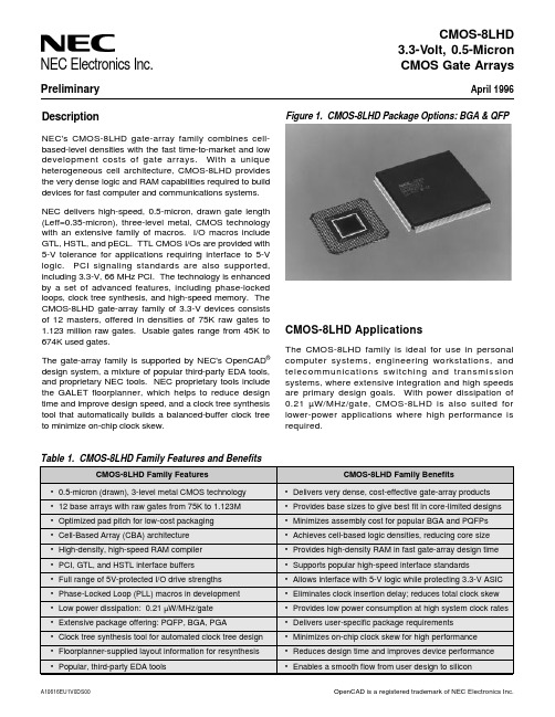
April 1996NEC Electronics Inc.A10616EU1V0DS00CMOS-8LHD3.3-Volt, 0.5-Micron CMOS Gate ArraysPreliminary DescriptionNEC's CMOS-8LHD gate-array family combines cell-based-level densities with the fast time-to-market and low development costs of gate arrays. With a unique heterogeneous cell architecture, CMOS-8LHD provides the very dense logic and RAM capabilities required to build devices for fast computer and communications systems.NEC delivers high-speed, 0.5-micron, drawn gate length (Leff=0.35-micron), three-level metal, CMOS technology with an extensive family of macros. I/O macros include GTL, HSTL, and pECL. TTL CMOS I/Os are provided with 5-V tolerance for applications requiring interface to 5-V logic. PCI signaling standards are also supported,including 3.3-V, 66 MHz PCI. The technology is enhanced by a set of advanced features, including phase-locked loops, clock tree synthesis, and high-speed memory. The CMOS-8LHD gate-array family of 3.3-V devices consists of 12 masters, offered in densities of 75K raw gates to 1.123 million raw gates. Usable gates range from 45K to 674K used gates.The gate-array family is supported by NEC's OpenCAD ®design system, a mixture of popular third-party EDA tools,and proprietary NEC tools. NEC proprietary tools include the GALET floorplanner, which helps to reduce design time and improve design speed, and a clock tree synthesis tool that automatically builds a balanced-buffer clock tree to minimize on-chip clock skew.Figure 1. CMOS-8LHD Package Options: BGA & QFPTable 1. CMOS-8LHD Family Features and BenefitsCMOS-8LHD ApplicationsThe CMOS-8LHD family is ideal for use in personal computer systems, engineering workstations, and telecommunications switching and transmission systems, where extensive integration and high speeds are primary design goals. With power dissipation of 0.21 µW/MHz/gate, CMOS-8LHD is also suited for lower-power applications where high performance is required.OpenCAD is a registered trademark of NEC Electronics Inc.CMOS-8LHD2Cell-Based Array ArchitectureThe CMOS-8LHD gate-array family is built with the Cell-Based Array (CBA) architecture licensed from the Silicon Architects Group of Synopsys. CBA architecture uses two types of cells: compute cells and drive cells.This heterogeneous cell architecture enables very high-density design. Compute cells are used to optimize intramacro logic. Drive cells are optimized for intermacro interconnect. The two cell types are also used to build macros with up to three different power/performance/area points.CBA has a rich macrocell library that is optimized for synthesis. RAM blocks are efficiently created from the CBA architecture, using compute cells as memory cores, and sense amplifiers and drive cells as word and address predecoder drivers.As shown in Figure 2, CBA is divided into I/O and array regions. The I/O region contains input and output buffers. The array region contains the gates used to build logic, RAM blocks, and other design features.Power Rail ArchitectureCMOS-8LHD provides additional flexibility for mixedvoltage system designs. As shown in Figure 2, the arrays contain two power rails: a 3.3-V rail, and V DD2.The V DD2 rail is used for interfaces such as 5-V PCI buffers where a clamping diode allows protection for up to an 11-V voltage spike, per the PCI revision 2.1specification.Figure 2. CBA Layout and Cell ConfigurationThe V DD2 rail is separated into sections to give flexibility for including two or more buses requiring special I/O voltage on one device. Each section can operate as an independent voltage zone, and sections can be linked together to form common voltage zones.Packaging and TestNEC utilizes BIST test structures for RAM testing. NEC also offers advanced packaging solutions including Plastic Ball Grid Arrays (PBGA), Plastic Quad Flat Packs (PQFP), and Pin Grid Arrays (PGA). Please call your local NEC ASIC design center representative for a listing of available master/package combinations.PublicationsThis data sheet contains preliminary specifications for the CMOS-8LHD gate-array family. Additional infor-mation will be available in NEC's CMOS-8LHD Block Library and CMOS-8LHD Design Manual . Call your local NEC ASIC design center representative or the NEC literature line for additional ASIC design information; see the back of this data sheet for locations and phone numbers.Table 2. CMOS-8LHD Base Array Line-upDevice Raw Gates Used Gates (1)Total Pads66562750404502416466563997925987518866565125216751292126656617963210777925266568202400121440268665692681281608763086657029792017875232466571359744215845356665725008643005184206657362054437232646866575802240481344532(1) Actual gate utilization varies depending on circuit implementation.Utilization is 60% for 3LM.3CMOS-8LHDInput/Output CapacitanceV DD =V I =0-V; f =1 MHzTerminal Symbol Typ Max Unit Input C IN 1020pF Output C OUT 1020pF I/OC I/O1020pF(1)Values include package pin capacitancePower ConsumptionDescription Limits Unit Internal gate (1)0.21µW/MHz Input buffer 2.546µW/MHz Output buffer10.60µW/MHzAbsolute Maximum RatingsPower supply voltage, V DD –0.5 to +4.6-VInput voltage, V I3.3-V input buffer (at V I < V DD + 0.5-V)–0.5 to +4.6-V 3.3-V fail-safe input buffer (at V I < V DD + 0.5-V)–0.5 to +4.6-V 5 V-tolerant (at V I < V DD + 3.0-V)–0.5 to +4.6-V Output Voltage, V O3.3-V output buffer (at V O < V DD + 0.5-V)–0.5 to +4.6-V 5-V-tolerant output buffer (at V O < V DD + 3.0-V)–0.5 to +4.6-V 5-V open-drain output buffer (at V O < V DD + 3.0-V)–0.5 to +4.6-VLatch-up current, I LATCH >1 A (typ)Operating temperature, T OPT –40 to +85°C Storage temperature, T STG–65 to +150°C (1) Assumes 30% internal gate switching at one timeCaution: Exposure to absolute maximum ratings for extended periods may affect device reliability; exceeding the ratings could cause permanent damage. The device should not be operated outside the recommended operating conditions.Recommended Operating ConditionsV DD = 3.3-V ±0.165-V; T j = 0 to +100°C3.3-V Interface 5-V Interface5-V PCI 3.3-V PCIBlock BlockLevel LevelParameterSymbol Min Max Min Max Min Max Min Max Unit I/O power supply voltage V DD 3.0 3.6 3.0 3.6 3.0 5.5 3.0 3.6V Junction temperature T J 0+1000+1000+1000+100°C High-level input voltage V IH 2.0V DD 2.0 5.5 2.0V CC 0.5 V CCV CC V Low-level input voltage V IL 00.800.800.800.3 V CCV Positive trigger voltage V P 1.50 2.70 1.50 2.70————V Negative trigger voltage V N 0.60 1.60.60 1.6————V Hysteresis voltage V H 1.10 1.3 1.10 1.3————V Input rise/fall time t R , t F 0200020002000200ns Input rise/fall time, Schmittt R , t F1010————nsAC CharacteristicsV DD = 3.3-V ±0.3-V; T j = –40 to +125°C ParameterSymbol MinTypMax Unit Conditions Toggle frequency (F611)f TOG356MHzD-F/F; F/O = 2 mmDelay time2-input NAND (F322)t PD181ps F/O = 1; L = 0 mmt PD 186ps F/O = 2; L = typ (0.42 mm)Flip-flop (F611)t PD 573ps F/O = 1; L = 0 mm t PD 688ps F/O = 2; L = typ t SETUP 410ps —t HOLD 540ps —Input buffer (FI01)t PD 268ps F/O = 1; L = 0 mm t PD 312ps F/O = 2; L = typ Output buffer (9 mA) 3.3-V (FO01)t PD 1.316ns C L = 15 pF Output buffer (9 mA) 5-V-tolerant (FV01)t PD 1.228ns C L = 15 pF Output buffer (9 mA) 5-V-swing (FY01)t PD 1.517ns C L = 15 pF Output rise time (9 mA) (FO01)t R 1.347ns C L = 15 pF Output fall time (9 mA) (FO01)t F1.284nsC L = 15 pFCMOS-8LHD4(3)Rating is for only one output operating in this mode for less than 1 second.(4)Normal type buffer: I OH < I OL .(5)Balanced buffer: I OH = I OL .(6)Resistor is called 50ký to maintain consistency with previous families.Notes:(1)Static current consumption increases if an I/O block with on-chip pull-up/pull-down resistor or an oscillator is used. Call an NEC ASIC design center repre-sentative for assistance in calculation.(2)Leakage current is limited by tester capabilities. Specification listed representsthis measurement limitation. Actual values will be significantly lower.DC CharacteristicsV DD = 3.3-V ±0.165-V; T j = 0 to +100°C ParameterSymbol Min Typ Max Unit Conditions Quiescent current (1)µPD66578I DDS 2.0300µA V I = V DD or GND µPD66575, 66573, 66572I DDS 1.0300µA V I = V DD or GND Remaining mastersI DDS 0.5200µA V I = V DD or GND Off-state output leakage current3.3-V buffers, 3.3-V PCII OZ ±10µA V O = V DD or GND 5-V-tolerant buffers, 5-V PCI I OZ ±14µA V O = V DD or GND 5-V open-drainI OZ ±14µA V O = V DD or GND Output short circuit current (3)I OS –250mA V O = GND Input leakage current (2)5-V PCI I IH +70, –70µA V IN = 2.7-V, 0.5-V 3.3-V PCI I I ±10µA V IN = V DD or GND RegularI I ±10–5±10µA V I = V DD or GND 50 k Ω pull-up I I –180–40µA V I = GND 5 k Ω pull-up I I –1400–350mA V I = GND 50 k Ω pull-down I I 30160µA V I = V DDResistor values50 k Ω pull-up (6)R pu 2075k Ω5 k Ω pull-upR pu 2.68.6k Ω50 k Ω pull-down (6)R pu 22.5100k ΩInput clamp voltageV IC –1.2V I I = 18 mA Low-level output current (ALL buffer types)3 mA I OL 3mA V OL = 0.4-V 6 mA I OL 6mA V OL = 0.4-V 9 mA I OL 9mA V OL = 0.4-V 12 mA I OL 12mA V OL = 0.4-V 18 mA I OL 18mA V OL = 0.4-V 24 mAI OL 24mA V OL = 0.4-V High-level output current (5-V-tolerant block)3 mA I OH –3mA V OH = V DD –0.4-V 6 mA I OH –3mA V OH = V DD –0.4-V 9 mA I OH –3mA V OH = V DD –0.4-V 12 mA I OH –3mA V OH = V DD –0.4-V 18 mA I OH –4mA V OH = V DD –0.4-V 24 mAI OH –4mA V OH = V DD –0.4-V High-level output current (3.3-V interface block)3 mA I OH –3mA V OH = V DD –0.4-V 6 mA I OH –6mA V OH = V DD –0.4-V 9 mA I OH –9mA V OH = V DD –0.4-V 12 mA I OH –12mA V OH = V DD –0.4-V 18 mA I OH -18mA V OH = V DD –0.4-V 24 mAI OH -24mA V OH = V DD –0.4-V Output voltage (5-V PCI)High-level output voltage V OH 2.4mA I OH = 2 mALow-level output voltage V OL 0.55mA I OL = 3 mA, 6 mA Output voltage (3.3-V PCI)High-level output voltage V OH 0.9 V DDmA I OH = 500 µA Low-level output voltage V OL 0.1 V DDmA I OL = 1500 µA Low-level output voltageV OL 0.1V I OL = 0 mA High-level output voltage, 5-V TTL V OH V DD –0.2V I OL = 0 mA High-level output voltage, 3.3-VV OHV DD –0.1VI OH = 0 mACMOS-8LHD5CMOS-8LHD6Document No. A10616EU1V0DS00For literature, call toll-free 7 a.m. to 6 p.m. Pacific time: 1-800-366-9782or FAX your request to: 1-800-729-9288©1996 NEC Electronics Inc./Printed in U.S.A.NEC ASIC DESIGN CENTERSWEST•3033 Scott Boulevard Santa Clara, CA 95054TEL 408-588-5008FAX 408-588-5017•One Embassy Centre9020 S.W. Washington Square Road,Suite 400Tigard, OR 97223TEL 503-671-0177FAX 503-643-5911THIRD-PARTY DESIGN CENTERSSOUTH CENTRAL/SOUTHEAST•Koos Technical Services, Inc.385 Commerce Way, Suite 101Longwood, FL 32750TEL 407-260-8727FAX 407-260-6227•Integrated Silicon Systems Inc.2222 Chapel Hill Nelson Highway Durham, NC 27713TEL 919-361-5814FAX 919-361-2019•Applied Systems, Inc.1761 W. Hillsboro Blvd., Suite 328Deerfield Beach, FL 33442TEL 305-428-0534FAX 305-428-5906NEC Electronics Inc.CORPORATE HEADQUARTERS2880 Scott Boulevard P.O. Box 58062Santa Clara, CA 95052TEL 408-588-6000No part of this document may be copied or reproduced in any form or by any means without the prior written consent of NEC Electronics Inc. (NECEL). The information in this document is subject to change without notice. ALL DEVICES SOLD BY NECEL ARE COVERED BY THE PROVISIONS APPEARING IN NECEL TERMS AND CONDITIONS OF SALES ONLY. INCLUDING THE LIMITATION OF LIABILITY,WARRANTY, AND PATENT PROVISIONS. NECEL makes no warranty, express, statutory, implied or by description, regarding informa-tion set forth herein or regarding the freedom of the described devices from patent infringement. NECEL assumes no responsibility for any errors that may appear in this document. NECEL makes no commitments to update or to keep current information contained in this document. The devices listed in this document are not suitable for use in applications such as, but not limited to, aircraft control systems,aerospace equipment, submarine cables, nuclear reactor control systems and life support systems. “Standard” quality grade devices are recommended for computers, office equipment, communication equipment, test and measurement equipment, machine tools,industrial robots, audio and visual equipment, and other consumer products. For automotive and transportation equipment, traffic control systems, anti-disaster and anti-crime systems, it is recommended that the customer contact the responsible NECEL salesperson to determine the reliabilty requirements for any such application and any cost adder. NECEL does not recommend or approve use of any of its products in life support devices or systems or in any application where failure could result in injury or death.If customers wish to use NECEL devices in applications not intended by NECEL, customer must contact the responsible NECEL sales people to determine NECEL’s willingness to support a given application.SOUTH CENTRAL/SOUTHEAST•16475 Dallas Parkway, Suite 380Dallas, TX 75248TEL 972-735-7444FAX 972-931-8680•Research Triangle Park2000 Regency Parkway, Suite 455Cary, NC 27511TEL 919-460-1890FAX 919-469-5926•Two Chasewood Park 20405 SH 249, Suite 580Houston, TX 77070TEL 713-320-0524FAX 713-320-0574NORTH CENTRAL/NORTHEAST•The Meadows, 2nd Floor 161 Worcester Road Framingham, MA 01701TEL 508-935-2200FAX 508-935-2234•Greenspoint Tower2800 W. Higgins Road, Suite 765Hoffman Estates, IL 60195TEL708-519-3945FAX 708-882-7564。

亞當斯級飛彈驅逐艦早期的亞當斯級使用MK-11雙臂發射器,圖為USS Henry B. Wilson(DDG-7)。
早期型亞當斯級的USS Barney(DDG-6)早期型亞當斯級的USS Robison(DDG-12)。
後期型的亞當斯級改用MK-13單臂發射器,圖為USS Cochraneu(DDG-21)。
德國向美國採購的亞當斯級,稱為呂特晏斯級(Lutjens class)。
此為首艦呂特晏斯號(Lütjens D-185),注意二號煙囪的第二桅杆與後方的SPS-52對空搜索雷達與亞當斯級不同,煙囪也為了避開SPS-52雷達天線而改成向兩側排氣。
澳洲向美國採購的三艘亞當斯級,稱為柏斯級(Perth class)。
圖為荷伯特號(HMAS Hobart D-39),注意艦體中部兩側各設置一座Ikara反潛飛彈發射器,並在艦舯增設一座艙室來容納Ikara反潛飛彈的彈艙。
另一張柏斯號的照片,攝於1990年代初的改良之後,原本設在兩舷彈藥艙室前方的Ikara反潛飛彈發射器遭到移除,二號煙囪兩側增設一對MK-15方陣近迫武器系統。
三艘澳洲柏斯級編隊航行,由前而後柏斯號、霍巴特號(HMAS Hobart DDG-39)與布里斯本號(HMAS Brisbane DDG-41)──by captain Picard主要參考資料:尖端科技雜誌270~272:冷戰時期美國海軍艦載防空系統發展──從3T的改良到NTU(張明德著)亞當斯級飛彈驅逐艦是美國海軍第一種飛彈驅逐艦,在1960到1980年代是美國海軍的防空主力之一,其艦體與動力系統的設計乃是以前一代薛曼級(Forrest Sherman class)驅逐艦為基礎。
最初美國還沒有「飛彈驅逐艦」(DDG)這個艦種,因此在1957年3月訂購的第一批八艘亞當斯級仍被視為艦隊型驅逐艦(DD),編號也接續於薛曼級之後,即DD-952~959。
在1956年8月16日,美國將當時規劃中的亞當斯級重新歸類為飛彈驅逐艦(DDG);在1957年5月23日,美國海軍將經過改裝、加裝防空飛彈系統的基靈級(Gearing class)驅逐艦蓋雅提號(USS USS Gyatt DDG-1 ex-DD-712)改歸類為飛彈驅逐艦(DDG),且舷號「歸零」從DDG-1開始,因此隨後亞當斯級的舷號便改由DDG-2排起。

编码解码芯片PT2262/PT2272芯片原理简介:PT2262/2272是台湾普城公司生产的一种CMOS工艺制造的低功耗低价位通用编解码电路,PT2262/2272最多可有12位(A0-A11)三态地址端管脚(悬空,接高电平,接低电平), 任意组合可提供531441地址码,PT2262最多可有6位(D0-D5)数据端管脚,设定的地址码和数据码从17脚串行输出,可用于无线遥控发射电路。
编码芯片PT2262发出的编码信号由:地址码、数据码、同步码组成一个完整的码字,解码芯片PT2272接收到信号后,其地址码经过两次比较核对后,VT脚才输出高电平,与此同时相应的数据脚也输出高电平,如果发送端一直按住按键,编码芯片也会连续发射。
当发射机没有按键按下时,PT2262不接通电源,其17脚为低电平,所以315MHz的高频发射电路不工作,当有按键按下时,PT2262得电工作,其第17脚输出经调制的串行数据信号,当17脚为高电平期间315MHz的高频发射电路起振并发射等幅高频信号,当17脚为低平期间315MHz的高频发射电路停止振荡,所以高频发射电路完全收控于PT2262的17脚输出的数字信号,从而对高频电路完成幅度键控(ASK调制)相当于调制度为100%的调幅。
PT2262/2272特点:CMOS工艺制造,低功耗,外部元器件少,RC振荡电阻,工作电压范围宽:2.6~15v ,数据最多可达6位,地址码最多可达531441种。
应用范围:车辆防盗系统、家庭防盗系统、遥控玩具、其他电器遥控。
名称管脚说明A0-A11 1-8、10-13 地址管脚,用于进行地址编码,可置为“0”,“1”,“f”(悬空), D0-D5 7-8、10-13 数据输入端,有一个为“1”即有编码发出,内部下拉Vcc 18 电源正端(+)Vss 9 电源负端(-)TE 14 编码启动端,用于多数据的编码发射,低电平有效;OSC1 16 振荡电阻输入端,与OSC2所接电阻决定振荡频率;OSC2 15 振荡电阻振荡器输出端;Dout 17 编码输出端(正常时为低电平)在具体的应用中,外接振荡电阻可根据需要进行适当的调节,阻值越大振荡频率越慢,编码的宽度越大,发码一帧的时间越长。

HSC277Silicon Epitaxial Planar Diode for UHF/VHF tuner Band SwitchADE-208-413 (Z)Rev. 0Dec. 1995 Features• Low forward resistance. (r f = 0.7max)• U l tra small F l at P a ckage (UFP) is suitable for surface mount design.Ordering InformationType No.Cathode Mark Package CodeHSC277Laser UFPOutlineAbsolute Maximum Ratings (Ta = 25°C)Item Symbol Value Unit35VReverse voltage VRJunction temperature Tj125°CPower dissipation Pd150mWOperation temperature Topr–20 to +60°CStorage temperature Tstg–45 to +125°CHSC2772Electrical Characteristics (Ta = 25°C)ItemSymbol Min Typ Max Unit Test Condition Reverse voltage V R 35——V I R = 10µA Reverse current I R ——50µA V R = 25V Forward voltage V F —— 1.0V I F = 10mA Capacitance C —— 1.2pF V R = 6V, f = 1MHz Forward resistancer f——0.7ΩI F = 2mA, f = 100MHzFig.1 Forward current Vs. Forward voltageHSC277Fig.2 Reverse current Vs. Reverse voltageFig.3 Capacitance Vs. Reverse voltage3HSC277Fig.4 Forward resistance Vs. Forward current 4HSC277 Package Dimensions5Cautions1.Hitachi neither warrants nor grants licenses of any rights of Hitachi’s or any third party’s patent,copyright, trademark, or other intellectual property rights for information contained in this document.Hitachi bears no responsibility for problems that may arise with third party’s rights, includingintellectual property rights, in connection with use of the information contained in this document.2.Products and product specifications may be subject to change without notice. Confirm that you have received the latest product standards or specifications before final design, purchase or use.3.Hitachi makes every attempt to ensure that its products are of high quality and reliability. However,contact Hitachi’s sales office before using the product in an application that demands especially high quality and reliability or where its failure or malfunction may directly threaten human life or cause risk of bodily injury, such as aerospace, aeronautics, nuclear power, combustion control, transportation,traffic, safety equipment or medical equipment for life support.4.Design your application so that the product is used within the ranges guaranteed by Hitachi particularly for maximum rating, operating supply voltage range, heat radiation characteristics, installationconditions and other characteristics. Hitachi bears no responsibility for failure or damage when used beyond the guaranteed ranges. Even within the guaranteed ranges, consider normally foreseeable failure rates or failure modes in semiconductor devices and employ systemic measures such as fail-safes, so that the equipment incorporating Hitachi product does not cause bodily injury, fire or other consequential damage due to operation of the Hitachi product.5.This product is not designed to be radiation resistant.6.No one is permitted to reproduce or duplicate, in any form, the whole or part of this document without written approval from Hitachi.7.Contact Hitachi’s sales office for any questions regarding this document or Hitachi semiconductor products.Hitachi, Ltd.Semiconductor & Integrated Circuits.Nippon Bldg., 2-6-2, Ohte-machi, Chiyoda-ku, Tokyo 100-0004, Japan Tel: Tokyo (03) 3270-2111 Fax: (03) 3270-5109Copyright ' Hitachi, Ltd., 1999. All rights reserved. Printed in Japan.Hitachi Asia Pte. Ltd.16 Collyer Quay #20-00Hitachi TowerSingapore 049318Tel: 535-2100Fax: 535-1533URLNorthAmerica : http:/Europe : /hel/ecg Asia (Singapore): .sg/grp3/sicd/index.htm Asia (Taiwan): /E/Product/SICD_Frame.htm Asia (HongKong): /eng/bo/grp3/index.htm Japan : http://www.hitachi.co.jp/Sicd/indx.htmHitachi Asia Ltd.Taipei Branch Office3F, Hung Kuo Building. No.167, Tun-Hwa North Road, Taipei (105)Tel: <886> (2) 2718-3666Fax: <886> (2) 2718-8180Hitachi Asia (Hong Kong) Ltd.Group III (Electronic Components)7/F., North Tower, World Finance Centre,Harbour City, Canton Road, Tsim Sha Tsui,Kowloon, Hong Kong Tel: <852> (2) 735 9218Fax: <852> (2) 730 0281 Telex: 40815 HITEC HXHitachi Europe Ltd.Electronic Components Group.Whitebrook ParkLower Cookham Road MaidenheadBerkshire SL6 8YA, United Kingdom Tel: <44> (1628) 585000Fax: <44> (1628) 778322Hitachi Europe GmbHElectronic components Group Dornacher Stra§e 3D-85622 Feldkirchen, Munich GermanyTel: <49> (89) 9 9180-0Fax: <49> (89) 9 29 30 00Hitachi Semiconductor (America) Inc.179 East Tasman Drive,San Jose,CA 95134 Tel: <1> (408) 433-1990Fax: <1>(408) 433-0223For further information write to:。

6073元器件交易网IMPORTANT NOTICETexas Instruments and its subsidiaries (TI) reserve the right to make changes to their products or to discontinueany product or service without notice, and advise customers to obtain the latest version of relevant informationto verify, before placing orders, that information being relied on is current and complete. All products are soldsubject to the terms and conditions of sale supplied at the time of order acknowledgement, including thosepertaining to warranty, patent infringement, and limitation of liability.TI warrants performance of its semiconductor products to the specifications applicable at the time of sale inaccordance with TI’s standard warranty. Testing and other quality control techniques are utilized to the extentTI deems necessary to support this warranty. Specific testing of all parameters of each device is not necessarilyperformed, except those mandated by government requirements.CERTAIN APPLICATIONS USING SEMICONDUCTOR PRODUCTS MAY INVOLVE POTENTIAL RISKS OFDEATH, PERSONAL INJURY, OR SEVERE PROPERTY OR ENVIRONMENTAL DAMAGE (“CRITICALAPPLICATIONS”). TI SEMICONDUCTOR PRODUCTS ARE NOT DESIGNED, AUTHORIZED, ORWARRANTED TO BE SUITABLE FOR USE IN LIFE-SUPPORT DEVICES OR SYSTEMS OR OTHERCRITICAL APPLICATIONS. INCLUSION OF TI PRODUCTS IN SUCH APPLICATIONS IS UNDERSTOOD TOBE FULLY AT THE CUSTOMER’S RISK.In order to minimize risks associated with the customer’s applications, adequate design and operatingsafeguards must be provided by the customer to minimize inherent or procedural hazards.TI assumes no liability for applications assistance or customer product design. TI does not warrant or representthat any license, either express or implied, is granted under any patent right, copyright, mask work right, or otherintellectual property right of TI covering or relating to any combination, machine, or process in which suchsemiconductor products or services might be or are used. TI’s publication of information regarding any thirdparty’s products or services does not constitute TI’s approval, warranty or endorsement thereof.Copyright © 1998, Texas Instruments Incorporated。


MCM 277 Quick Start GuideWhat’s in the Box?You should find these items upon opening the box.Mounting stand onto the set 123Put MCM277 on a flat and firm surface, rear side facing upAs shown, align the stand to the slots at set’s bottom, 4 FRONT facing downPush the stand down into the slotsRear connectionsConnect the cable of the left speaker to LEFT (red and black) and the cable of the right speaker to RIGHT (red and black)1Helpful hints:- For wall mounting, please refer to the User Manual , Appendix: How to mount your MCM277 onto Walls. You may need assistance from the qualified service personnel.Setting the clock 12345In the standby mode, press and hold DISPLAY/CLOCK on the remote control➜ 24 HR or 12 HR appears for the initial clock setting. T o select 12-hour clock or 24-hour clock,a. Press VOL +/- once or moreb. Press DISPLAY/CLOCK to confirm ➜ The hours digits start flashingHold down or press VOL +/- repeatedly to set the hoursPress DISPLA Y/CLOCK to confirmHold down or press VOL +/- repeatedly to set the minutesPress DISPLAY/CLOCKto confirm123Playing discsWith this system, you can play all pre-recorded audio CDs (CDDA), all finalized audio CD-Rsand CD-RWs, MP3/WMA-CDs (CD-Rs/CD-RWs with MP3/WMA files)Press SOURCE once or more to select CD (or CD on the remote control)Press CD OPEN•CLOSE ç to open the CD compartmentInsert a disc with the printed side facing up. Press CD OPEN•CLOSE ç again to close the compartmentNotes for remote control:–First, select the source you wish to control by pressing one of the source select keys on the remote control (DISC or TUNER, for example).–Then select the desired function ( 2;, 4, ¢ for example).IMPORTANT!– Remove the protective plastic tab before using the remote controlTuning to radio stations 123123Check you have unfolded the control panelInsert the USB device’s USB plug into the socketon the set ‘s foldable control panelPress SOURCE once or more to select USB (or USB on the remote control)PDCC-JW-0801C Royal Philips Electronics N.V . 2008All rights reserved. Detailed playback features and additional functions are described in the accompanied owner's manual.Press SOURCE once or more to select TUNER (or TUNER on the remote control)Press and hold PROG until AUTO appears➜ flashes. Available stations are programmed: RDS stations followed by FM stations, MW stationsPress the 3/ 4 buttons once or more until the desired preset station is displayedPlaying a USB mass storage deviceWith the Hi-Fi system, you can use USB flash memory (USB 2.0 or USB1.1),USB flash players (USB 2.0 or USB1.1), memory cards (requires an additional card reader to work with this Hi-Fi system).4Play the USB’s audio files as you do with the albums/tracks on a CD5Press STANDBY -ON y to switch off the set。


©2002 Whelen Engineering Company Inc.Form No.13739 (121002)51 Winthrop Road Chester, Connecticut 06412-0684Phone: (860) 526-9504Internet: Salese-mail:*******************CustomerServicee-mail:******************M a s sNo t if ica t ion ®ENGINEERING COMPANY INC.For warranty information regarding this product, visit /warrantyS.A.M.Siren Activation Monitoring Software Software GuideOverview...The SAM (Siren Activation and Monitoring) software, combined with the SAMI (Siren Activation and Monitoring Interface) module, allows a user to control and monitor from 1 to 10,000 individual siren sites from within a Microsoft Windows environment (Windows 2000 or higher). The SAM software uses highly detailed maps, onto which sirens are precisely positioned, along with their theoretical areas of coverage. With all sirens in place, the user can test or activate groups or individual sirens. This can be accomplished through manual control or automated activation through the use of individual, custom Call Keys.Although this software has been designed for ease of use, it is necessary for the user to thoroughly read and understand this manual before using the SAM software. This manual assumes the user has a basic understanding of the Windows operating system.IMPORTANT! The user must be logged into Windows as an administrator before this software can be used. Logging In...Before the configuration portions of the SAM software can be used, a user must be logged in. Until a user is logged in, Settings, Siren, Call Key and Mapping commands are not available. Logging in is accomplished as follows:1.Start the SAM program.2.Go to File>Configuration Log In. This opens the Configuration Log In window. Here the user will beprompted to enter a password as shown below:If a password has not yet been specified, the user may click on the OK button without entering a password. This will log the current user in and unlock the configuration features. No password is required until a password has been specified. To specify a password, click on the Change Password check box. This will expand the Configuration Log In window to include new information fields; New Password and Confirm Password. Leaving the Password field blank, enter the desired password in the New Password field. The user must then re-enter the exact same password in the Confirm Password field. IMPORTANT! When selecting a password any alpha-numeric characters (including spaces) are acceptable, but keep in mind that the password is case sensitive. Remember to write the password down and keep it in a safe, secure place. In the event of the password being lost, contact Whelen Engineering.Maps and map layers...After logging in for the first time, a map must be generated. This is accomplished by loading layers into the software. This step is only required to be performed once, as the layers (and the map they in turn generate) will be subsequently loaded whenever the software is started. Each layer contains specific map elements. For example, one layer may contain state and national parks, while another layer may contain all public buildings and schools. A layer may be configured to be visible or not visible, depending on the degree of detail the user wishes to be displayed.1.Got to Mapping>Layer Control. This will open the Layer Control window:As shown, 3 layers will be pre-loaded; Siren Layer, 60dB Layer and 70dB Layer. The mapping layers must now be added to the map.2.Click on the Add button. From the open window, navigate to the following address:C:\Documents and Settings\All Users\Application Data\Whelen\SAM\MapsNote:The ‘Application Data’ folder is a system folder and is hidden by default. System and Hidden folders and files can not be hidden for this procedure. Consult your windows operating system guide on changing this parameter.3.Select all of the *.TAB files in this folder. HINT: Hold the Ctrl key and click once on each file to select multiplefiles. With all the files highlighted, click the Open button. As the screen will now show, the mapping layers have now been added to the map.ing the Up button, move the Siren Layer, 60dB Layer and 70dB Layer to the top of the layers list.With the layers successfully loaded, the Radio and Station settings must now be configured.Radio and Station settings...Configuring the Radio and Station settings is accomplished by clicking on Settings>Radio and Settings>Station respectively. In each window, click the OK button after the appropriate information has been entered.Adding and working with sirens...Adding a siren1.Click on Siren>Add Siren to open the Siren Configuration window:In this window the user will configure the type of siren being added to the map. Configuration consists of defining siren address, the options present on the siren in question, the siren type, the siren model and, if required, the Latitude & Longitude of the sirens location. Please refer to your siren manual for further information on siren features and addressing. IMPORTANT! Each station’s address must be a unique number. If latitude & longitude values are not entered, and the Add to Map box is checked, the siren will be located at the center of your display.Deleting a siren1.Locate the list of siren address in the column on the left side of the screen. Click on the address of the siren tobe deleted.2.Click on Siren>Delete Siren. The user will then be reminded that a siren is about to be deleted. If the correctsiren was highlighted in Step 1, click the Yes button to delete the siren. If the wrong siren was selected in Step 1, Click No to abort the command.Configure/Inquire sirenClick on Siren>Configure/Inquire Siren to review or change information pertaining to a specific siren. The following window will open:This window is similar to the Siren Configuration window, with the additional display of the Activation and Response Log data.Call Keys...A Call Key offers the user an easy way to handle routine siren station activations. Essentially, a Call Key automates the execution of a series of command instructions. For demonstration purposes, this section will outline the steps used to create a Call Key that will be used to issue tornado warnings. In this example, the following siren equipment is in use: Siren #1WPS4003(Address 1001)Siren #2WPS4003(Address 1002)Siren #3WPS4003(Address 1003)When this Call Key, named Tornado Warning, is activated, the following events will occur:•Rotate all sirens to NORTH (allow 35 seconds to complete this task).•Broadcast DV1 (allow 30 seconds to complete this task).•Rotate all sirens to EAST (allow 10 seconds to complete this task).•Broadcast DV1 (allow 30 seconds to complete this task).•Rotate all sirens to SOUTH (allow 10 seconds to complete this task).•Broadcast DV1 (allow 30 seconds to complete this task).•Rotate all sirens to WEST (allow 10 seconds to complete this task).•Broadcast DV1 (allow 30 seconds to complete this task).•Broadcast the Alert tone (allow 3 minutes to complete this task)•Send the Clear command to all sirens (allow 2 seconds to complete this taskThe steps required to create this sequence of events are presented here in a step-by-step format.1.Click on Call Keys>Add Call Key to open the following window:In the Call Key Name text box, enter Tornado Warning and place a checkmark in the Activation check box.2.Click the Add button to create the Call Key.The Tornado Warning call key being created will be used to activate the siren. In this example the user will place a check mark in the Activation box. If the Call Key is to be used as part of a routine, automated test, the user would place a check in the Time of Day box. When this box is checked, the dialog window changes to allow the user to select the frequency of this particular system test.If the Call Key being created is to be activated with an external contact closure, the dialog window changes to allow the user to select which one of three available external contact closures will initiate this Call Key.Regardless of the Call Key type being selected, the subsequent programming procedures are the same.3.After clicking Add, a new window will appear. Here, the user will create the sequences that will comprise theTornado Warning Call Key.4.Sequence 1 - The first sequence requires all sirens to be rotated to face North. To accomplish this, the userplaces a checkmark in the North check box in the Rotor section.All sirens are required to face North. To accomplish this the user will click the All (####) button. This will add four ‘Wild Cards’ to the Siren Address text box (refer to your siren manual for an explanation of siren addressing protocols and Wild Cards).The user must allow sufficient time for all the sirens to rotate to the North before progressing to the next sequence. To accomplish this, the user will enter 35 in the Time Until Next Sequence text box.After all the data for this first sequence has been entered, the user will click on the Add Sequence button in the Add/Edit section of the window. The window will now display Sequence 1 in the table in the lower portion of the window as shown:5.Sequence 2- The second sequence requires all sirens to broadcast Digital Voice Message 1(DV1). Toaccomplish this the user places a checkmark in the DV1Check Box in the Digital Voice section of the window.All sirens are required to broadcast this message, so the 4 ‘Wild Cards’ will be left in the Siren Address section.The user must allow sufficient time for the message to be completed. In this example, DV1 takes 28 seconds to complete. The user will enter 30 in the Time Until Next Sequence text box.After all the data for Sequence 2 has been entered, the user will click on the Add Sequence button in the Add/Edit section of the window. This will add Sequence 2 to the table in the lower portion of the window as shown:6.Sequence 3 - The third sequence requires all sirens to be rotated to face East. To accomplish this, the userplaces a checkmark in the East check box in the Rotor section.All sirens are required to face East. To accomplish this the user will click the All (####) button. This will add four ‘Wild Cards’ to the Siren Address text box (refer to your siren manual for an explanation of siren addressing protocols and Wild Cards).The user must allow sufficient time for all the sirens to rotate to the East before progressing to the next sequence. Since prior to the execution of this sequence, all sirens were facing North, it will not take as long to orient the sirens to face to the East. The user will enter 10 in the Time Until Next Sequence text box.After all the data for Sequence 3 has been entered, the user will click on the Add Sequence button in the Add/Edit section of the window. The window will now display Sequence 3 in the table in the lower portion of the window as shown:7.Sequence 4- The second sequence requires all sirens to broadcast Digital Voice Message 1(DV1). Toaccomplish this the user places a checkmark in the DV1Check Box in the Digital Voice section of the window.All sirens are required to broadcast this message, so the 4 ‘Wild Cards’ will be left in the Siren Address section.The user must allow sufficient time for the message to be completed. In this example, DV1 takes 28 seconds to complete. The user will enter 30 in the Time Until Next Sequence text box.After all the data for Sequence 4 has been entered, the user will click on the Add Sequence button in the Add/Edit section of the window. This will add Sequence 4 to the table in the lower portion of the window as shown:8.Sequence 5 - Follow the same procedure used for Sequence 3, using South as the desired direction.9.Sequence 6 - Follow the same procedure used for Sequence 4.10.Sequence 7 - Follow the same procedure used for Sequence 3, using West as the desired direction.11.Sequence 8 - Follow the same procedure used for Sequence 4.12.Sequence 9 - This sequence requires all sirens to broadcast the Alert siren tone for 3 minutes. To accomplishthis, the user places a checkmark in the Alert check box.All sirens are required to broadcast this tone, so the 4 ‘Wild Cards’ will be left in the Siren Address section.This tone must be broadcast for 3 minutes. The user will enter 180 in the Time Until Next Sequence text box.13.Sequence 10 - This sequence will send the Clear command to the siren. To accomplish this, the user willplace a checkmark in the Clear check box.All sirens are to receive this command, so the 4 ‘Wild Cards’ will be left in the Siren Address section.The Clear command will be broadcast for 2 seconds. The user will enter 2 in the Time Until Next Sequence text box.After all the data for Sequence 10 has been entered, the user will click on the Add Sequence button in the Add/Edit section of the window. This will add Sequence 10 to the table in the lower portion of the window. 14.The user will now click the Done button to complete the programming procedure and close this window.This Call Key is completed and ready to be used. Activation Call Keys are activated by clicking on the Activation Call Key pull-down list located in the upper right area of the program window. Select the desired Call Key. The user will be presented with the option of either sending the selected Call Key sequence or aborting without transmitting the sequence.Editing a Sequence - If a particular sequence needs to be edited, the user will select the desired sequence by clicking on the grey bar preceding the sequence to be edited. In this example, Sequence 5 is to be edited.After the desired changes have been made, the user must then click the Update Sequence button in the Add/Edit section. Click the Done button to complete the editing procedure and close this window.Deleting a Sequence - If a sequence needs to be deleted the user would highlight the sequence to be deleted. The user would then click the Delete Sequence button. After all the designated sequences have been deleted, click the Done button to complete the editing procedure and close this window.Inserting a Sequence - If an additional sequence needs to be added, the user would highlight the sequence where the new sequence is to be inserted. After all the data for the new sequence has been entered, the user will click on the Insert Sequence button to insert the new sequence.。
HSU277Silicon Epitaxial Planar Diode for UHF/VHF tuner Band SwitchADE-208-018G(Z)Rev 6Nov. 1998 Features• Low forward resistance. (rf = 0.7Ω max)• U l tra small R e sin P a ckage (URP) is suitable for surface mount design.Ordering InformationType ser Mark Package CodeHSU2773URPOutlineHSU2772Absolute Maximum Ratings (Ta = 25°C)ItemSymbol Value Unit Reverse voltage V R 35V Power dissipation Pd 150mW Junction temperature Tj 125°C Storage temperature Tstg -45 to +125°C Operation temperatureTopr-20 to +60°CElectrical Characteristics (Ta = 25°C)ItemSymbol Min Typ Max Unit Test Condition Reverse voltage V R 35——V I R = 10µA Forward voltage V F —— 1.0V I F = 10 mA Reverse current I R ——50nA V R = 25VCapacitance C —— 1.2pF V R = 6V, f = 1 MHz Forward resistancer f——0.7ΩI F = 2 mA, f = 100 MHzHSU277 Main Characteristic3HSU277Package DimensionsUnit : mm4Cautions1.Hitachi neither warrants nor grants licenses of any rights of Hitachi’s or any third party’s patent,copyright, trademark, or other intellectual property rights for information contained in this document.Hitachi bears no responsibility for problems that may arise with third party’s rights, includingintellectual property rights, in connection with use of the information contained in this document.2.Products and product specifications may be subject to change without notice. Confirm that you have received the latest product standards or specifications before final design, purchase or use.3.Hitachi makes every attempt to ensure that its products are of high quality and reliability. However,contact Hitachi’s sales office before using the product in an application that demands especially high quality and reliability or where its failure or malfunction may directly threaten human life or cause risk of bodily injury, such as aerospace, aeronautics, nuclear power, combustion control, transportation,traffic, safety equipment or medical equipment for life support.4.Design your application so that the product is used within the ranges guaranteed by Hitachi particularly for maximum rating, operating supply voltage range, heat radiation characteristics, installationconditions and other characteristics. Hitachi bears no responsibility for failure or damage when used beyond the guaranteed ranges. Even within the guaranteed ranges, consider normally foreseeable failure rates or failure modes in semiconductor devices and employ systemic measures such as fail-safes, so that the equipment incorporating Hitachi product does not cause bodily injury, fire or other consequential damage due to operation of the Hitachi product.5.This product is not designed to be radiation resistant.6.No one is permitted to reproduce or duplicate, in any form, the whole or part of this document without written approval from Hitachi.7.Contact Hitachi’s sales office for any questions regarding this document or Hitachi semiconductor products.Hitachi, Ltd.Semiconductor & Integrated Circuits.Nippon Bldg., 2-6-2, Ohte-machi, Chiyoda-ku, Tokyo 100-0004, Japan Tel: Tokyo (03) 3270-2111 Fax: (03) 3270-5109Copyright ' Hitachi, Ltd., 1999. All rights reserved. Printed in Japan.Hitachi Asia Pte. Ltd.16 Collyer Quay #20-00Hitachi TowerSingapore 049318Tel: 535-2100Fax: 535-1533URLNorthAmerica : http:/Europe : /hel/ecg Asia (Singapore): .sg/grp3/sicd/index.htm Asia (Taiwan): /E/Product/SICD_Frame.htm Asia (HongKong): /eng/bo/grp3/index.htm Japan : http://www.hitachi.co.jp/Sicd/indx.htmHitachi Asia Ltd.Taipei Branch Office3F, Hung Kuo Building. No.167, Tun-Hwa North Road, Taipei (105)Tel: <886> (2) 2718-3666Fax: <886> (2) 2718-8180Hitachi Asia (Hong Kong) Ltd.Group III (Electronic Components)7/F., North Tower, World Finance Centre,Harbour City, Canton Road, Tsim Sha Tsui,Kowloon, Hong Kong Tel: <852> (2) 735 9218Fax: <852> (2) 730 0281 Telex: 40815 HITEC HXHitachi Europe Ltd.Electronic Components Group.Whitebrook ParkLower Cookham Road MaidenheadBerkshire SL6 8YA, United Kingdom Tel: <44> (1628) 585000Fax: <44> (1628) 778322Hitachi Europe GmbHElectronic components Group Dornacher Stra§e 3D-85622 Feldkirchen, Munich GermanyTel: <49> (89) 9 9180-0Fax: <49> (89) 9 29 30 00Hitachi Semiconductor (America) Inc.179 East Tasman Drive,San Jose,CA 95134 Tel: <1> (408) 433-1990Fax: <1>(408) 433-0223For further information write to:。