合科泰常规厚膜片式电阻器规格书
- 格式:pdf
- 大小:1.42 MB
- 文档页数:11
厚膜贴片电阻的原理、特点和应用厚膜贴片电阻是一种常见的被动元件,它是利用厚膜工艺将电阻性材料印刷在绝缘基体(如氧化铝陶瓷)上,然后经过高温烧结而成的。
厚膜贴片电阻具有体积小、功率大、耐热、耐冲击和耐腐蚀等优点,广泛应用于各种电子设备中,如智能手机、平板电脑、笔记本电脑、电视、汽车、医疗和军事设备等。
厚膜贴片电阻的原理厚膜贴片电阻的原理是利用电阻性材料的电阻率随温度的变化而变化的特性,通过控制印刷的厚度和图案,来调节电阻值。
电阻性材料一般是由金属粉末(如银、钯、铂等)和玻璃粉末混合而成的浆料,通过丝网印刷工艺将其印刷在绝缘基体上,形成一层或多层的厚膜。
厚膜的厚度一般在10微米到100微米之间,因此称为厚膜。
然后,将印刷好的基体放入高温炉中进行烧结,使浆料中的金属粉末和玻璃粉末熔化并固化,形成具有一定电阻率的均匀薄膜。
最后,通过激光切割或化学刻蚀等方法,在厚膜上切割出所需的图案,从而确定电阻值。
同时,在基体的两端印刷出导电性材料(如银或银钯合金),作为与外部电路连接的焊盘。
厚膜贴片电阻的特点厚膜贴片电阻具有以下几个主要特点:体积小、功率大。
由于厚膜贴片电阻是直接印刷在绝缘基体上,因此可以做到非常小的尺寸,如0075、01005、0201等。
同时,由于厚膜贴片电阻具有较高的耐热性和散热性,因此可以承受较大的功率,如0.125W、0.25W、0.5W等。
耐热、耐冲击和耐腐蚀。
由于厚膜贴片电阻采用了高温烧结工艺,因此具有较高的稳定性和可靠性,可以在-55℃到+155℃的温度范围内正常工作,并且不易受到机械冲击和化学腐蚀的影响。
适用于所有焊接工艺。
由于厚膜贴片电阻具有较高的耐热性和导电性,因此可以适应各种焊接工艺,如波峰焊、回流焊、手工焊等,并且在自动贴片应用中具有较高的稳定性和一致性。
成本低、产量高。
由于厚膜贴片电阻采用了丝网印刷工艺,因此可以实现批量生产,降低生产成本和时间。
同时,由于厚膜贴片电阻的材料和工艺相对简单,因此可以提供较多的规格和参数,满足不同的应用需求。
片式电阻尺寸表一、尺寸定义片式电阻尺寸采用英制单位,主要包括长、宽和厚度三个维度。
长和宽的尺寸以英寸为单位,而厚度尺寸则以英寸的字母缩写表示。
例如,0201表示片式电阻的长和宽均为0.02英寸,而厚度的尺寸则由数字后面的字母来表示,如M表示0.125英寸,K表示0.156英寸等。
二、尺寸规格以下是一些常见的片式电阻尺寸规格:1.0201:长×宽×厚为0.02×0.02×0.125英寸。
2.0402:长×宽×厚为0.04×0.02×0.125英寸。
3.0603:长×宽×厚为0.06×0.03×0.156英寸。
4.0805:长×宽×厚为0.08×0.05×0.156英寸。
5.1206:长×宽×厚为0.12×0.06×0.2英寸。
这些规格中的数字代表了片式电阻的长和宽的尺寸,单位为英寸。
例如,0201表示片式电阻的长和宽均为0.02英寸,而厚度的尺寸则由数字后面的字母来表示,如M表示0.125英寸,K表示0.156英寸等。
三、尺寸与功率关系一般来说,片式电阻的尺寸越大,其所能承受的功率也就越大。
因此,在选择电阻时,需要根据实际应用场景选择合适的尺寸以满足功率需求。
四、尺寸与精度关系片式电阻的尺寸越大,其精度通常越高。
这是因为较大的电阻通常具有更均匀的阻值分布和更小的温度系数。
因此,在需要高精度的应用场景下,可以选择较大的片式电阻。
五、尺寸与温度系数关系片式电阻的尺寸也会影响其温度系数。
一般来说,较大的片式电阻具有更小的温度系数,即其阻值随温度的变化更小。
因此,在需要稳定性的应用场景下,可以选择较大的片式电阻。
综上所述,选择合适的片式电阻尺寸需要考虑实际应用场景中的功率、精度和稳定性等因素。
根据这些因素选择合适的片式电阻尺寸可以更好地满足实际需求。
No.: RPCH-K-HTS-0001 /2Date: 2017.4.21Data sheetTitle: FIXED THICK FILM CHIP RESISTORS; RECTANGULAR TYPE AND HIGH POWER ⋅ ANTI SURGEStyle: RPCH16,20,32,35AEC-Q200 qualifiedRoHS COMPLIANCE ITEMHalogen and Antimony FreeNote: ・Stock conditionsTemperature: +5°C ∼+35°CRelative humidity: 25% ∼ 75%The period of guarantee: Within 2 year from shipmen t by the company.Solderability shall be satisfied.・Product specification contained in this data sheetare subject to change at any time without notice・If you have any questions or a Purchasing Specification for any quality Agreement is necessary, please contact our sales staff. ArrayHokkaido Research CenterApproval by: T. SannomiyaDrawing by: M. Shibuya1. Scope1.1 This data sheet covers the detail requirements for fixed thick film chip resistors; rectangular type & high power ⋅ anti surge,style of RPCH16,20,32,35.1.2 Applicable documentsJIS C 5201−1: 2011, JIS C 5201−8: 2014, JIS C 5201−8−1: 2014 IEC60115−1: 2008, IEC60115−8: 2009, IEC60115−8−1: 2014 EIAJ RC −2134C −20102. ClassificationType designation shall be the following form.(Example) RPCH 32 K 123 J TP 1 2 3 4 5 6 Style1 Fixed thick film chip resistors; rectangular type & & high power ⋅ anti surge2 Rated dissipation and / or dimension3 T emperature coefficient of resistance4 Rated resistance123 E24 Series, 3 digit, Ex. 123--> 12k Ω, 1000 E96 Series, 4 digit, Ex. 1000-->100Ω1022--> 10.2k Ω5 T olerance on rated resistanceD ±0.5% F ±1% J ±5%6 Packaging formB Bulk (loose package) TP Paper taping TE Embossed tapingK ±100×10−6/ °C−(Dash ) Standard Style3. Rating3.1 The ratings shall be in accordance with T able −1.T able −1StyleRated dissipation (W) T emperature coefficient of resistance (10-6 / °C) Rated resistance range (Ω)Preferred number series for resistors T olerance on rated resistance RPCH160.33K ±100 10∼1M E24, 96 D(±0.5%), F(±1%) Standard ±200 1.0∼9.76 K ±100 10∼1M E24 J(±5%) Standard ±200 1.0∼9.1 RPCH20 0.5K ±100 10∼1M E24, 96 D(±0.5%), F(±1%) Standard ±200 1.0∼9.76 K ±100 10∼1M E24 J(±5%) Standard ±200 1.0∼9.1 RPCH32 0.66K ±100 10∼1M E24, 96 D(±0.5%), F(±1%) Standard ±200 1.0∼9.76 K ±100 10∼1M E24 J(±5%) Standard ±200 1.0∼9.1 RPCH35 0.75K ±100 10∼1M E24, 96 D(±0.5%), F(±1%) Standard ±200 1.0∼9.76 K ±100 10∼1M E24J(±5%)Standard±200 1.0∼9.1Style Limiting element voltage(V) Isolation voltage(V) Category temperaturerange(°C)RPCH16 150150 −55~+155RPCH20200500RPCH32 RPCH353.2 Climatic category55/155/56 Lower category temperature − 55 °C Upper category temperature +155 °C Duration of the damp heat, steady state test 56days 3.3 Stability class5% Limits for change of resistance:−for long −term tests ±(5%+0.1Ω) −for short −term tests ±(1%+0.05Ω)3.4 DeratingFigure–1 Derating curveAmbient temperature (°C)3.5 Rated voltaged.c.or a.c.r.m.s.voltage calculated from the square root of the product of the rated resistance and the rated dissipation. E: Rated voltage (V)E =P ·RP: Rated dissipation (W) R: Rated resistance (Ω)Limiting element voltage can only be applied to resistors when the resistance value is equal to or higher than the criticalresistance value.At high value of resistance, the rated voltage may not be applicable.4. Packaging formThe standard packaging form shall be in accordance with T able −2.T able −2Symbol Packaging form Standard packagingquantity / unitsApplicationB Bulk (loose package) 1,000 pcs .RPCH16,20,32,35 TP Paper taping 8mm width, 4mm pitches 5,000 pcs. RPCH16,20,32TE Embossed taping8mm width, 4mm pitches 4,000 pcs. RPCH355. Dimensions5.1 The resistor shall be of the design and physical dimensions in accordance with Figure −2 and T able −3.Figure −2T able −3 Unit: mmStyle L W H c d RPCH16 1.6±0.1 +0.15 0.8 -0.05 0.45±0.10 0.3±0.2 0.3±0.1 RPCH20 2.0±0.1 1.25±0.10 0.55±0.10 0.3±0.2 0.4±0.2 RPCH32 3.1±0.1 1.6±0.15 0.55±0.10 0.4±0.25 0.5±0.25 RPCH35 3.1±0.15 2.5±0.15 0.55±0.15 0.4±0.25 0.5±0.255.2 Net weight (Reference)Style Net weight(mg) RPCH16 2 RPCH20 5 RPCH32 9 RPCH35 166. MarkingResistorThe Rated resistance shall be marked in 3 digits (E24) or 4 digits (E96) and marked on over coat side.• E24 series: 3 digits, E96 series: 4 digitsIn case of the resistance value that E96 overlaps with E24, It is marked by either.The Rated resistance of RPCH16 should not be marked in 4 digits(E96)Marking example Contents Application123 12×10 3 [Ω]→ 12 [kΩ]E24(RPCH16,20,32,35)2R2 2. 2[Ω]E24(RPCH 16,20,32,35)5623 562 ×103 [Ω] → 562 [kΩ] E96(RPCH 20,32,35)12R7 12.7 [Ω] E96(RPCH 20,32,35)7. Performance7.1 The standard condition for tests shall be in accordance with Sub−clause 4.2, JIS C 5201−1: 2011.7.2 The performance shall be satisfied in T able−4.T able−4(1)No. T est items Condition of test (JIS C 5201−1) Performance requirements1 Visual examination Sub−clause 4.4.1Checked by visual examination. As in 4.4.1The marking shall be legible, as checked by visual examination.2 DimensionResistance Sub−clause 4.4.2Sub−clause 4.5As specified in T able−3 of thisspecification.As in 4.5.2The resistance value shallcorrespond with the rated resistancetaking into account the specifiedtolerance.3 Voltage proof Sub−clause 4.7Method: 4.6.1.4T est voltage: Alternating voltage with a peakvalue of 1.42 times the insulationvoltage.Duration: 60 s ± 5 sInsulation resistanceT est voltage: Insulation voltageDuration: 1 min. No breakdown or flash over R ≥ 1 G Ω4 Solderability Sub−clause 4.17Without ageingFlux: The resistors shall be immersed in anon−activated soldering flux for 2s.Bath temperature: 235 °C ± 5 °CImmersion time: 2 s ± 0.5 s As in 4.17.4.5The terminations shall be covered with a smooth and bright solder coating.T able −4(2)No T est items Condition of test (JIS C 5201−1)Performance requirements 5Mounting Overload (in the mounted state) Solvent resistance of the marking Sub −clause 4.31 Substrate material: Epoxide woven glass Sub −clause 4.13 The applied voltage shall be 2.5 times the rated voltage or twice the limiting element voltage, whichever is the less severe. Duration: 2 s Visual examination ResistanceSub −clause 4.30 Solvent: 2−propanolSolvent temperature: 23 °C ± 5 °C Method 1Rubbing material: cotton wool Without recoveryNo visible damage ∆R ≤ ± (1%+0.05Ω) Legible marking6Mounting Bound strength of the end face plating Final measurements Sub −clause 4.31 Substrate material: Epoxide woven glass Sub −clause 4.33 Bent value: 3 mm Resistance Sub −clause 4.33.6 Visual examination∆R ≤ ± (1%+0.05Ω) No visible damage7Resistance to soldering heat Component solvent resistance Sub −clause 4.18 Solder temperature: 260 °C ± 5 °C Immersion time: 10 s ± 0.5 s Visual examination Resistance Sub −clause 4.29 Solvent: 2−propanolSolvent temperature: 23 °C ± 5 °C Method 2Recovery: 48 h Visual examination ResistanceAs in 4.18.3.4No sign of damage such as cracks. ∆R ≤ ± (1%+0.05Ω)No visible damage ∆R ≤ ± (1%+0.05Ω)T able −4(3)No T est itemsCondition of test (JIS C 5201−1)Performance requirements 8MountingAdhesionRapid change temperatureSub −clause 4.31Substrate material: Epoxide woven glass Sub −clause 4.32 Force: 5 NDuration: 10 s ± 1 s Visual examination Sub −clause 4.19Lower category temperature:−55 °C Upper category temperature:+155 °CDuration of exposure at each temperature: 30 min.Number of cycles: 5 cycles. Visual examination ResistanceNo visible damageNo visible damage ∆R ≤ ±(1%+0.05Ω) 9Climatic sequence −Dry heat−Damp heat, cycle (12+12hour cycle) First cycle−Cold−Damp heat, cycle (12+12hour cycle) Remaining cycle−D.C. loadSub −clause 4.23 Sub −clause 4.23.2T est temperature: +155 °C Duration: 16 h Sub −clause 4.23.3 T est method: 2T est temperature: 55 °C [Severity(2)]Sub −clause 4.23.4T est temperature −55 °C Duration: 2hSub −clause 4.23.6 T est method: 2T est temperature: 55 °C [Severity (2)]Number of cycles: 5 cycles Sub −clause 4.23.7The applied voltage shall be the rated voltage or the limiting element voltage whichever is the smaller.Duration: 1 min. Visual examination ResistanceNo visible damage ∆R ≤ ± (5%+0.1Ω) 10MountingEndurance at 70 °C Sub −clause 4.31Substrate material: Epoxide woven glass Sub −clause 4.25.1Ambient temperature: 70 °C ± 2 °C Duration: 1000 hThe voltage shall be applied in cycles of 1.5 h on and 0.5 h.The applied voltage shall be the rated voltage or the limiting element voltage whichever is the smaller.Examination at 48 h , 500 h and 1000 h:Visual examination ResistanceNo visible damage ∆R ≤ ± (5%+0.1Ω)T able −4(4)No T est items Condition of test (JIS C 5201−1)Performance requirements 11Mounting V ariation of resistance with temperature Sub −clause 4.31 Substrate material: Epoxide woven glass Sub −clause 4.8 −55 °C / +20 °C+20 °C / +155°CAs in T able −112Mounting Damp heat, steady state Sub −clause 4.31 Substrate material: Epoxide woven glass Sub −clause 4.24Ambient temperature: 40 °C ± 2 °C +2 Relative humidity : 93 % −3 a) 1st group: without voltage applied.b) 2nd group: The d. c. voltage shall be appliedcontinuously .The voltage shall be accordance with Sub −clause 4.24.2.1 b). without polarizing voltage [4.24.2.1, c)] Visual examinationResistanceNo visible damage Legible marking ∆R ≤ ± (5%+0.1Ω) 13Dimensions (detail) Mounting Endurance at upper category temperature Sub −clause 4.4.3 Sub −clause 4.31 Substrate material: Epoxide woven glass Sub −clause 4.25.3 Ambient temperature:155 °C ± 2 °CDuration: 1000 hExamination at 48 h, 500 h and 1000 h:Visual examination Resistance As in T able −3No visible damage ∆R ≤ ± (5%+0.1Ω)8. T aping8.1 Applicable documents JIS C 0806−3: 2014, EIAJ ET −7200C: 2010 8.2 T aping dimensions8.2.1 T aping dimensions shall be in accordance with Figure −3 and T able −5.Unit: mmFigure −3T able −5 Unit: mmStyle A B t 1 t 2 RPCH16 1.15±0.15 1.9±0.2 0.6±0.1 0.8max. RPCH20 1.65±0.15 2.5±0.2 0.8±0.1 1.0max. RPCH32 2.00±0.15 3.6±0.2 0.8±0.1 1.0max.8.2.2 Embossed taping dimensions shall be in accordance with Figure −4 and T able −6.Unit: mmFigure −4T able −6 Unit: mmStyle A B W E t 1 RPCH35 2.85±0.20 3.5±0.2 8.0±0.3 3.5±0.05 1.0±0.21). The cover tapes shall not cover the sprocket holes.2). T apes in adjacent layers shall not stick together in the packing. 3). Components shall not stick to the carrier tape or to the cover tape. 4). Pitch tolerance over any 10 pitches ±0.2mm.5). The peel strength of the top cover tape shall be with in 0.1N to 0.5N on the test method as shown in the followingRPCH16,20,32:Figure −4,RPCH35:Figure-5.6). When the tape is bent with the minimum radius for 25 mm, the tape shall not be damaged and the components shallmaintain their position and orientation in the tape.7). In no case shall there be two or more consecutive components missing.The maximum number of missing components shall be one or 0.1%, whichever is greater. 8). The resistors shall be faced to upward at the over coating side in the carrier cavity .Figure −5Figure −6/min )165°to180°Carrier tape T op cover tapeP eel −off(About 300mm /min )Direction of unreelingNo: RPCH −K −HTS −0001 /2Title:FIXED THICK FILM CHIP RESISTORS; RECTANGULAR TYPE ANDHIGH POWER ⋅ ANTI SURGE RPCH16,20,32,35Page: 10/10Product specification contained in this data sheet are subject to change at any time without notice.If you have any questions or a Purchasing Specification for any quality agreement is necessary, please contact our sales staff.Issue: KAMAYA ELECTRIC CO., LTD. Research & Development Department HOKKAIDO Research center Last update: 2017.4.218.3 Reel dimensionReel dimensions shall be in accordance with the following Figure −7 and T able −7.T able −7 Unit: mmStyleA B Note RPCH16,20,32,35 +1.0 9 011.4±1.0 Injection molding13±1.0 V acuum formingNote : Marking label shall be marked on a place of Marking A or two place of marking A and B.Figure −89. Marking on packageThe label of a minimum package shall be legibly marked with follows. 9.1 Marking A(1) Classification(Style, T emperature coefficient of resistance, Rated resistance, T olerance on rated resistance, Packaging form)(2) Quantity (3) Lot number (4) Manufacturer’s name or trade mark (5) Others9.2 Marking B (KAMA Y A control label)。
片式厚膜电阻器片式厚膜电阻器,是一种常见的电阻器类型,具有许多优点和广泛的应用。
本文将从厚膜电阻器的原理、结构、特点和应用等方面进行介绍。
一、厚膜电阻器的原理厚膜电阻器是利用厚膜工艺在陶瓷或玻璃基片上制作电阻材料,再通过蒸镀、丝印等工艺形成导线和引线,最后在高温烧结过程中形成电阻器结构。
厚膜电阻器的电阻值由电阻材料的阻值、长度和宽度决定。
二、厚膜电阻器的结构厚膜电阻器一般由基片、电阻材料、电极、引线和封装等部分组成。
基片作为电阻器的基础,一般采用陶瓷或玻璃材料;电阻材料是通过厚膜工艺在基片上制作的,常见的材料有铬、铜、镍等;电极是连接电阻材料的导线,常见的形式有蒸镀、丝印等;引线是将电阻器连接到电路中的导线,一般采用金属材料;封装是将电阻器保护起来,常见的封装有贴片式、插件式等。
三、厚膜电阻器的特点1. 高精度:厚膜电阻器的电阻值精度高,一般可达到1%或更高。
2. 耐高温:厚膜电阻器可以在高温环境下工作,一般可耐受几百摄氏度的温度。
3. 耐腐蚀:厚膜电阻器的电阻材料往往具有良好的耐腐蚀性能,可以在恶劣的环境下使用。
4. 体积小:厚膜电阻器的体积相对较小,适合在空间有限的电路中使用。
5. 成本低:相比于其他类型的电阻器,厚膜电阻器的制造成本相对较低。
四、厚膜电阻器的应用厚膜电阻器广泛应用于各种电子设备和电路中,主要包括以下几个方面:1. 电源供应:厚膜电阻器常用于电源供应电路中的电流限制、电压分压等功能。
2. 信号处理:厚膜电阻器用于信号处理电路中的电流测量、电阻匹配等。
3. 温度测量:厚膜电阻器可以作为温度传感器使用,常用于温度测量和控制中。
4. 自动控制:厚膜电阻器常用于自动控制电路中的反馈、调节和保护等功能。
5. 通信设备:厚膜电阻器用于通信设备中的阻抗匹配、滤波等。
片式厚膜电阻器是一种常见的电阻器类型,具有高精度、耐高温、耐腐蚀、体积小和成本低等特点。
它广泛应用于电子设备和电路中的电源供应、信号处理、温度测量、自动控制和通信设备等领域。
片式电阻尺寸表
一般情况下,片式电阻的尺寸表包括以下几个参数:
1. 长度(Length):片式电阻的整体长度,通常以毫米(mm)为单位。
2. 宽度(Width):片式电阻的整体宽度,通常以毫米(mm)为单位。
3. 厚度(Thickness):片式电阻的整体厚度,通常以毫米(mm)为单位。
4. 电阻面积(Resistance Area):片式电阻器的电阻发热区域
的面积,通常以平方毫米(mm²)为单位。
5. 电阻值(Resistance Value):片式电阻器的电阻值,通常以欧姆(Ω)为单位。
6. 容差(Tolerance):片式电阻器的电阻值允许的偏差范围,通常以百分比形式表示。
7. 最大功率(Maximum Power):片式电阻器能够承受的最大功率,通常以瓦特(W)为单位。
需要注意的是,片式电阻的尺寸表可能会因不同的制造商、型号和尺寸而有所差异,上述参数仅为常见参数,具体以实际产品规格为准。
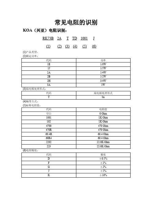
常见电阻的识别KOA(兴亚)电阻识别:RK73B2A T TD1001J(1)(2)(3)(4)(5)(6)(1)产品类型:(2)额定功率:代码功率1E1/8W1J1/5W2A1/4W2B1/2W2H3/4W3A1W (3)端电极处理形式:代码端电极处理形式T Sn(4)编带方式:(5)标称电阻值:代码电阻值空白0Ohm10011K Ohm1021K Ohm4700470Ohm470R470Ohm60.4R60.4Ohm60R460.4Ohm220222.0K Ohm22322.0K Ohm (6)电阻精度:代码精度D±0.5%F±1%G±2%J±5%K±10%ROHM(罗姆)电阻识别:MCR01MZP J102(1)(2)(3)(4)(5)(1)电阻类型:代码类型MCR厚膜电阻器PMR金属盘电阻器ESR抗波动型厚膜电阻器KTR耐高压厚膜电阻器MNR网络型厚膜电阻器RCN贴片式衰减型厚膜电阻器MVR贴片式微条型厚膜电阻器(2)封装尺寸、功率及耐压:代码型号英制长×宽功率耐压00602010.6×0.3mm1/20W25V 010402 1.0×0.5mm1/16W50V 030603 1.6×0.8mm1/10W50V 100805 2.0×1.25mm1/8W150V (3)元件个数:代码个数JZH4000EZH5000HZP2000EZP5000MZP10000YZP15000EOAP5000MOAP10000HXBR2000IXBR3000KXBR5000(4)电阻精度:代码精度D±0.5%F±1%G±2%J±5%K±10%(5)标称电阻值:代码电阻值0000Ohm1021K Ohm UNIOHM(厚声)电阻识别:1206S4J012J T5E(1)(2)(3)(4)(5)(6)(7)(1)封装尺寸:型号公制型号英制长×宽050302010.5×0.25mm10050402 1.0×0.5mm16080603 1.5×0.76mm20120805 2.0×1.25mm32161206 3.2×1.6mm32251210 3.2×2.5mm45321812 4.5×3.2mm (2)额定功率:代码功率WM1/20WWG1/16WWA1/10WW81/8WW41/4WW21/2W073/4W1W1W1A1/10WSS81/8WSS41/4W-SU21/2WSSS21/2W-S073/4W-S(3)电阻精度:代码精度D±0.5%F±1%G±2%J±5%(4)标称电阻值:代码电阻值100210K Ohm10011K Ohm00000Ohm012J 1.2Ohm012K0.12Ohm012L0.012Ohm注:前三位表示有效数字,后一位表示有几个0,其中J=0.1,K=0.01,L=0.001。
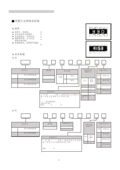
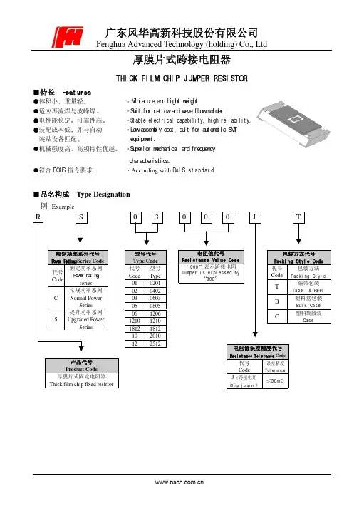
特性 FEATURES品名构成 Type Designation体积小、重量轻。
适应再流焊与波峰焊。
电性能稳定,可靠性高。
装配成本低,并与自动装贴设备匹配。
机械强度高、高频特性优越。
Miniature and light weight.Suit for reflow and wave flow solder.Stable electrical capability, high reliability.Low assembly cost, suit for automatic SMTequipment.Superior mechanical and frequencycharacteristics.例1 Example 1例2 Example 2RCML08W103JTML0610R103JT厚膜片式网络电阻器THICK FILM CHIP NETWORK RESISTORTHICK FILM CHIP NETWORK RESISTOR参考标准 REFERENCE STANDARD结构图 CONSTRUCTIONIEC E-24 系列电阻值代码对照表 GB/T 5729-94GB/T 9546-1995JIS C 5223-1989JIS C 5201-1994JIS C 5202-1985IEC E-24 Series Resistance Cross-reference Listn E-24 系列 E-24 Series (×10Ω)(单位unit:1Ω、10Ω、100Ω、1KΩ、10KΩ、100KΩ、1MΩ)6.二次玻璃 2nd cover glass5. 一次玻璃 1st cover glass4. 电阻体 resistive element3. 面电极 face electrode7. 端电极 inner termination8. 中间电极 Middle termination2. 背电极 reverse side electrode1. 陶瓷基片 ceramic substrate9. 外部电极 outer termination6. 二次玻璃 2nd cover glass5. 一次玻璃 1st cover glass4. 电阻体 resistive element3. 面电极 face electrode7. 端电极 inner termination8. 中间电极 Middle termination2. 背电极 reverse side electrode1. 陶瓷基片 ceramic substrate9. 外部电极 outer termination例1 Example 1:RCMT/RCML/RCMC:例2 Example 2:ML06/ML12:THICK FILM CHIP NETWORK RESISTOR规格尺寸及等效电路 DIMENSIONS AND EQUIVALENT CIRCUIT例1 Example 1:RCMT/RCML/RCMC:R1R2R3R4R1=R2=R3=R4R1R2R1=R2例2 Example 2:ML06/ML12:SRR1R5R1=R2=R3=R4=R5=R6=R7=R8负荷下降曲线 DERATING CURVE当电阻使用的环境温度超过70℃时,其额定负荷(额定功率或额定电流)按上述曲线下降。
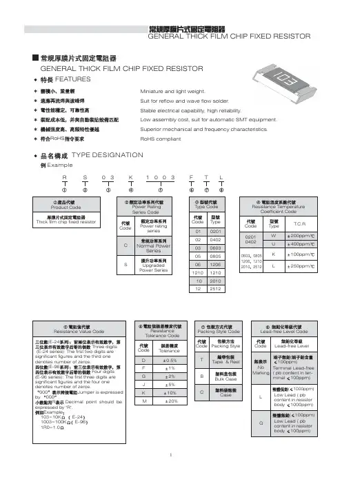
FEATURESGENERAL THICK FILM CHIP FIXED RESISTORRoHSTYPE DESIGNATIONExampleGENERAL THICK FILM CHIP FIXED RESISTORMiniature and light weight.Suit for reflow and wave flow solder.Stable electrical capability,high reliability.Low assembly cost,suit for automatic SMT equipment.Superior mechanical and frequency characteristics.RoHS compliantCONSTRUCTION AND DIMENSIONLaWtbunit:mmAPPEARANCE,The surface of resistor is covered with Protective Coating which hard to fade,and the surface of coating should avoid unevenness.The terminal part is covered equable ,the plating is hard to fade,and should avoid unevenness,flaw,pinhole and discoloration.With a clear mark ,the resistor body is crack-free.REFERENCE STANDARDGB/T 5729-2003GB/T 9546-1995DERATING CURVE70()For resistors operated in ambient over 70,rated load (power rating or current rating)shall be deratedin accordance with the above figure.1007550-55-50-25255075100125175Ambient temperature()P e r c e n t r a t e d l o a dGENERAL THICK FILM CHIP FIXED RESISTOR150RATINGSPACKAGINGTape and reelPaper taping 02010402GENERAL THICK FILM CHIP FIXED RESISTOR0603080512061210Embossed tapingP P1W FEA0B0D0P0D1tA0K0K0B0tP P1WFEABD0P0TRemark:For0201type,T1refers to the hole depth of paper carrier tape,T refers to the thickness of the paper carrier tape.ReelDMWTGENERAL THICK FILM CHIP FIXED RESISTORBulk casePACKAGING QUANTITYunit:mm110313612GENERAL THICK FILM CHIP FIXED RESISTORThe Explanation For The Resistance Value MarkingIEC E-24E-96IEC E-24E-96Series Resistance Cross-reference ListE-24E-24series10nunit1101001K10K100K1M10MTable oneE-2410E-24series:Express resistance value on the glass side with three digits,the first tow digits should be significant and the third one denote number of zeros.ExampleE-96Example0603E-96For the dimension type of 0603,express the resistance value with three code,the first two digit code denote the resistance of E-96series,and the third code of letter denote the multiplier (see the table three and four ).ExampleR The decimal point should be expressed by .R ExampleThe jumper should be expressed by 0Example02010402For the dimension type of 02010402,there is no mark on the glass side.ExampleIEC IEC E-24For the resistancewhich don't belong to IEC serial,use the resistance of IEC serial which is most close to the required resistance of non-IEC serial for replacement.To get agreement by both party if there special requirement for the marking.10K100K2M5.610E-96series:For the dimension type of 0805,1206,12102010,2512express the resistance value with four digits,the first three digits are significant figures and the fourth denotes the number of zeros.,GENERAL THICK FILM CHIP FIXED RESISTOR Table threeE-96E-96series resistance value codeTable fourMultiplied code11。
承认书APPROV AL SHEET客户名称:CUSTOMER品名:常规厚膜片式固定电阻器PARTNAME规格版本号VERSION日期DATE制造客户APPROV AL APPROV AL 拟制审核确认检验审核批准序号No目录TABLE OF CONTENTS1.0 概述Summary2.0 结构及尺寸Structure And Dimensions3.0 型号规格表示办法How To Order4.0 电气性能Performance Specification5.0 可靠性Reliability Data6.0 包装Package7.0 环保情况说明Environmental Protection Statement8.0 推荐使用的焊接曲线Recommended soldering profile9.0 使用注意事项Precautions For UseRC/RS□□□□1.0概述Summary片式电阻器主要生产的型号包括01005、0201、0402、0603、0805、1206、1210、2010、2512。
其特点是:The dimension type for chip resistor including01005、 0201、0402、0603、0805、1206、1210、2010、2512, and the features are as below:*体积小、重量轻miniature and light weight*电性能稳定,可靠性高 stable electrical capability and high reliability *机械强度高、高频特性优越superior mechanical and frequency*装配成本低,并与自动贴装设备匹配low assembly cost, suit for automatic SMT *适应再流焊与波峰焊suit for re-flow and wave flow soldering .*符合ROHS指令要求Compliant with ROHS Directive*符合无卤素要求Compliant with halogen free requirement*禁止使用SS-00259中规定的1级环境管理物质*SONY指定原材料只能从绿色伙伴认定供应商处采购产品广泛应用于计算机、通讯、工业自动化、航天航空、军事、数字电视、数字音响及消费类电子等领域。
1.品名的构成例如:RI0603L1003FTRI 0603 L 1003 F T2.结构1.外保护层2.字码印记3.内保护层4.阻体层5.导体层6.侧面导体层7.镀镍层8.镀锡层9. 陶瓷基体2 3 4 5 6 7 8 913.尺寸和电性参数4.字码4.1 (大于1Ω表示方法)*0201、0402 因电阻本体太小,固无印记表示。
*公差为±0.1%、±0.5%、±1%的用四位数表示,前三位表示有效数字,第四位表示乘幂(10V)。
例如1003=100X103=100X1000=100000Ω=100KΩ4703=470X103.=470X1000=470000Ω=470KΩ22R1=22.1Ω(R表示小数点)1R30=1.3Ω(R表示小数点,不足四位在后面加0)*公差为±2%、±5%、用三位数表示,前二位数表示有效数字,第三位数表示乘幂(10V)。
例如103=10X103=10X1000=10000Ω=10KΩ473=47X103.=47X1000=47000Ω=47KΩ1R3=1.3Ω(R表示小数点)*E96代码表示, 公差为±0.1%、±0.5%、±1%用三位数表示(仅对0603表示)例如02C=102X102=102X100=10200Ω=10.2KΩ15E=140X104=140X10000=1400000Ω=1.4MΩ*公差为±0.1%、±0.5%、±1%(仅对0603表示)在E-24 系列中,但不属于E-96系列的阻值,标示和±5%的公差相同,但是在字码下多加一条横线.例如:124=120K4.2 (小于1Ω表示方法)*0201、0402 因电阻本体太小,固无印记表示。
*公差为±0.1%、±0.5%、±1%的用四位数表示,R表示小数点。
例如R200=0.2ΩR002=0.002Ω*公差为±2%、±5%、用三位数表示,R表示小数点。
• Small size & light weight 短小轻薄• Reduction of assembly costs and matching with placement machine. 可降低装置成本及配合机器组装• Suitable for both wave & re-flow soldering. 适合波峰焊与回流焊• Applications: Navigator (GPS), Mobile Phone,Telecom, PDA, Setbox, Meter. 应用于GPS , 移动电话,PDA ,机顶盒,仪表Feature (特性)Figures (型状)Derating Curve & Specification降功率曲线及性能Thick Film Chip ResistorsP e r c e n t r a t e d l o a d (%)Ambient termperature 环境温度 (°C)厚膜晶片电阻器负载比率(%)UniOhm3r i g h s e rv ed .©UValue阻值Code 代码Value 阻值Code 代码Value 阻值Code 代码Value 阻值Code 代码Value 阻值Code 代码Value 阻值Code 代码100011471721533316494646568181102021501822134324504756669882105031541922635332514876771583107041582023236340524996873284110051622123737348535116975085113061652224338357545237076886115071692324939365555367178787118081742425540374565497280688121091782526141383575627382589124101822626742392585767484590127111872727443402595907586691130121912828044412606047688792133131962928745422616197790993137142003029446432626347893194140152053130147442636497995395143162103230948453646658097696Thick Film Chip Resistors• For 0201 & 0402 size, no marking on the body due to the small size of the resistor. 0201, 0402因电阻本体太小,故本体无标示字码• ±5% tolerance product: the marking is 3 digits, the first 2 digits are the significant of theresistance and the 3rd digit denotes number of zeros following.±5%公差产品字码是三位数,前二位是阻值的有效数,第三位表示有几个 0• 0805, 1206, 1210, 2010, 2512 ≤±1%: the marking is 4 digits, the first 3 digits are the significant of the resistance and the 4th digit denotes number of zeros following. 0805, 1206, 1210, 2010, 2512 ≤±1%公差产品字码有四位数,前三位是阻值的有效数,第四位表示有几个 0Marking on the Resistors Body (电阻本体字码标示)2372 = 23700Ω = 23.7KΩBelow 10Ω : 3R24 = 3.24Ω10Ω 以下标示: 3R24 = 3.24Ω153 = 15000Ω = 15KΩBelow 10Ω: 6R8 = 6.8Ω10Ω 以下标示: 6R8 = 6.8Ω• Standard E-96 series values of 0603 ≤±1%: due to the small size of the resistor’s body, 3 digits marking will be used to indicate the accurate resistance value by using the following Multiplier & Resistance Code.0603 ≤±1%公差 E-96系列标准阻值,因电阻本体太小,采用三位阻值代码(数字)及下列指数代码(字母)配合来指明标准的阻值。
2018产品说明书PRODUCT MANUAL深圳市叁叶源主要生产被动元器件SMD R‐Chip 电阻,产品尺寸:0402‐1206,阻值范围:1‐22兆欧姆,产品具有高可靠性电极设计、兼容所有焊接制程等特点。
Administrator深圳市叁叶源电子有限公司2018/6/1目录Contents●特点Features3●品名构成Type Designation3●结构Construction4●规格尺寸Dimensions4●负荷下降曲线Derating Curve4●额定值Ratings5●常规TCR值5●高精度TCR±50额定值6●特性Characteristics6●推荐焊盘尺寸Recommend Solder Pad Size9●包装Packaging9●IEC E-24、E-96系列电阻值代码对照表12●厚膜电阻阻值代码及标记规则14●片式电阻器使用说明16●焊接Soldering17■常规厚膜片式固定电阻器General Thick Film Chip Fixed Resistor●特点Features体积小、重量轻Miniature and light weight 适应再流焊与波峰焊Suit for reflow and wave flow solder 电性能稳定,可靠性高Stable electrical capability,high reliability 装配成本低,并与自动贴装设备匹配Low assembly cost,suit for automatic SMT equipment 机械强度高,高频特性优越Superior mechanical and frequency characteristics 符合RoHS 指令要求Compliant with RoHS directive 符合无卤素Halogen free requirement●品名构成Type Designation Single Chip ResistorSY 0402J N 100R P (1)(2)(3)(4)(5)(6)(1)(2)(3)(4)(5)(6)SeriesSize Reslstance Toleiance TCRResistance Packing style SY Thinck Film ST Thinck FilmSA Atuomotive Garde0402060308051206B=±0.1%D=±0.5%F=±1%J=±5%N=Base on Spc E=±50ppm/℃D=±25ppm/℃F=±100ppm/℃G=±200ppm/℃1K 100K 10R 4K71MP=Pager TapeB=Embossed Plastic●结构Construction①陶瓷基板Ceramic Substrate ②背电极Bottom Electrode ③面电极Top Electrode ④电阻体Resistor Layer ⑤一次保护Primary Overcoat ⑥二次保护Secondary Overcoat ⑦端电极Edge Electrode ⑧中间电极Barrier Layer ⑨外部电极External Electrode●规格尺寸Dimensions型号Type 尺寸Dimensions(mm)L W t a b 0402 1.00±0.100.50±0.050.35±0.050.20±0.100.25±0.100603 1.60±0.100.80±0.100.45±0.100.30±0.200.30±0.200805 2.00±0.15 1.25+0.15-0.100.55±0.100.40±0.200.40±0.2012063.10±0.151.55+0.15-0.100.55±0.100.45±0.200.45±0.20●负荷下降曲线Derating Curve额定负荷百分比Percent Rated Load环境温度Ambient temperature(℃)使用温度范围:OperatingTemperature Range:①-55℃~125℃②-55℃~155℃注1:图中曲线适用于适用于0402、0603、0805、1206。