X5045中文资料
- 格式:pdf
- 大小:1.17 MB
- 文档页数:6

监控芯片X5045的应用作者:杜洋2005-10-13X5045是一种3合1功能监控芯片,其具有EEPROM、电压跌落检测、看门狗复位。
用SPI总线与处理器通信,是兼有储存监测的单片机系统的最佳选择。
X5045的特性如下:·支持MOTOROLA推出的SPI总线协议·可选复位时间的看门狗定时器·电源电压跌落检测和复位控制·5种标准的开始复位电压·当电源电压为1V时仍可保证复位输出·多种芯片选择不同的工作电压·内置4Kbit的EEPROM,可擦写100万次·EEPROM数据可全部或分区保护·硬件及指令写保护,使数据更安全·时钟可达3.3MHZ·读写速度快,16字节的页写入·经典写周期为5mS·商用级温宽为0~70摄氏度,工业级温宽为-40~84摄氏度·16字节的页写入模式·复位信号输出可保持200MSX5045接口说明:1-CS/WDI使能及看门狗复位输入2-SO数据输出(可与SI复用)3-WP写保护(低电平保护)4-Vss参考0电位5-SI数据输入6-SCK时钟输入7-RESET复位信号输出(必须接上接电阻)8-Vcc电源电压X5045与单片机接口电路:通信协议:在每一次通信之前都必须输入2个字节的操作数据。
其中有9位是操作地址位,3位功能选择位。
操作位在第5到第7个时钟脉冲输入,地址位在第4个脉冲为最高地址,第8到第23个时钟脉冲输入由高到低的8位地址数据。
地址结构为:“0 0 0 0 A8 M2 M1 M0 A7 A6 A5 A4 A3 A2 A1 A0”(A为地址,M为功能)。
其第1个字节的功能选择表如下:读数据操作:写数据操作:状态寄存器的说明:X5045内置一个状态寄存器,用于设置看门狗和数据锁存。
其为8位数据,有单独的功能操作数据。
当读写状态寄存器时地址位数据就成为状态寄存器的数据镜像。


4K X5043/X5045512 x 8 BitCPU Supervisor with 4K SPI EEPROMFEATURES•Selectable time out watchdog timer•Low V CC detection and reset assertion—Five standard reset threshold voltages—Re-program low V CC reset threshold voltage using special programming sequence.—Reset signal valid to V CC = 1V•Long battery life with low power consumption —<50µA max standby current, watchdog on —<10µA max standby current, watchdog off —<2mA max active current during read• 2.7V to 5.5V and 4.5V to 5.5V power supply versions•4Kbits of EEPROM–1M write cycle endurance •Save critical data with Block Lock™ memory —Protect 1/4, 1/2, all or none of EEPROM array •Built-in inadvertent write protection—Write enable latch—Write protect pin• 3.3MHz clock rate•Minimize programming time—16-byte page write mode—Self-timed write cycle—5ms write cycle time (typical)•SPI modes (0,0 & 1,1)•Available packages—8-lead MSOP, 8-lead SOIC, 8-pin PDIP—14-lead TSSOP DESCRIPTIONThese devices combine four popular functions, Power-on Reset Control, Watchdog Timer, Supply Voltage Supervision, and Block Lock Protect Serial EEPROM Memory in one package. This combination lowers system cost, reduces board space requirements, and increases reliability.Applying power to the device activates the power on reset circuit which holds RESET/RESET active for a period of time. This allows the power supply and oscil-lator to stabilize before the processor executes code. The Watchdog Timer provides an independent protec-tion mechanism for microcontrollers. When the micro-controller fails to restart a timer within a selectable time out interval, the device activates the RESET/ RESET signal. The user selects the interval from three preset values. Once selected, the interval does not change, even after cycling the power.The device’s low V CC detection circuitry protects the user’s system from low voltage conditions, resetting the system when V CC falls below the minimum V CC trip point. RESET/RESET is asserted until V CC returns to proper operating level and stabilizes. Five industry standard V TRIP thresholds are available, however, Xicor’s unique circuits allow the threshold to be repro-grammed to meet custom requirements or to fine-tune the threshold for applications requiring higher precision.BLOCK DIAGRAMSISOSCK CS/WDIV CC RESET/RESETWPX5043 = RESETX5045 = RESETX5043/X5045The memory portion of the device is a CMOS Serial EEPROM array with Xicor’s block lock protection. The array is internally organized as x 8. The device features a Serial Peripheral Interface (SPI) and software proto-col allowing operation on a simple four-wire bus.The device utilizes Xicor’s proprietary Direct Write™cell, providing a minimum endurance of 1,000,000 cycles and a minimum data retention of 100 years.PIN CONFIGURATIONPIN DESCRIPTIONSSerial Output (SO)SO is a push/pull serial data output pin. During a read cycle, data is shifted out on this pin. Data is clocked out by the falling edge of the serial clock.Serial Input (SI)SI is the serial data input pin. All opcodes, byte addresses, and data to be written to the memory are input on this pin. Data is latched by the rising edge of the serial clock.Serial Clock (SCK)The Serial Clock controls the serial bus timing for data input and output. Opcodes, addresses, or data present on the SI pin is latched on the rising edge of the clock input, while data on the SO pin changes after the fall-ing edge of the clock input.Chip Select (CS)When CS is high, the X5043/45 is deselected and the SO output pin is at high impedance and, unless an internal write operation is underway, the X5043/45 will be in the standby power mode. CS low enables the X5043/45, placing it in the active power mode. It should be noted that after power-up, a high to low transition on CS is required prior to the start of any operation.Write Protect (WP)When WP is low, nonvolatile writes to the X5043/45 are disabled, but the part otherwise functions normally. When WP is held high, all functions, including non vol-atile writes operate normally. WP going low while CS is still low will interrupt a write to the X5043/45. If the internal write cycle has already been initiated, WP going low will have no affect on a write.Reset (RESET, RESET)X5043/45, RESET/RESET is an active low/HIGH, open drain output which goes active whenever V CC falls below the minimum V CC sense level. It will remain active until V CC rises above the minimum V CC sense level for 200ms. RESET/RESET also goes active if the Watchdog timer is enabled and CS remains either high or low longer than the Watchdog time out period. A fall-ing edge of CS will reset the watchdog timer.PIN NAMESSymbol Description CS Chip Select InputSO Serial OutputSI Serial InputSCK Serial Clock InputWP Write Protect InputV SS GroundV CC Supply Voltage RESET/RESET Reset OutputX5043/X5045PRINCIPLES OF OPERATIONPower On ResetApplication of power to the X5043/X5045 activates a Power On Reset Circuit. This circuit pulls the RESET/ RESET pin active. RESET/RESET prevents the sys-tem microprocessor from starting to operate with insuf-ficient voltage or prior to stabilization of the oscillator. When V CC exceeds the device V TRIP value for 200ms (nominal) the circuit releases RESET/RESET, allowing the processor to begin executing code.Low Voltage MonitoringDuring operation, the X5043/X5045 monitors the V CC level and asserts RESET/RESET if supply voltage falls below a preset minimum V TRIP. The RESET/RESET signal prevents the microprocessor from operating in a power fail or brownout condition. The RESET/RESET signal remains active until the voltage drops below 1V. It also remains active until V CC returns and exceeds V TRIP for 200ms.Watchdog TimerThe Watchdog Timer circuit monitors the microproces-sor activity by monitoring the WDI input. The micropro-cessor must toggle the CS/WDI pin periodically to prevent an active RESET/RESET signal. The CS/WDI pin must be toggled from HIGH to LOW prior to the expiration of the watchdog time out period. The state of two nonvolatile control bits in the Status Register determines the watchdog timer period. The micropro-cessor can change these watchdog bits. With no microprocessor action, the watchdog timer control bits remain unchanged, even during total power failure.V CC Threshold Reset ProcedureThe X5043/X5045 is shipped with a standard V CC threshold (V TRIP) voltage. This value will not change over normal operating and storage conditions. How-ever, in applications where the standard V TRIP is not exactly right, or if higher precision is needed in the V TRIP value, the X5043/X5045 threshold may be adjusted. The procedure is described below, and uses the application of a high voltage control signal.Setting the V TRIP VoltageThis procedure is used to set the V TRIP to a higher volt-age value. For example, if the current V TRIP is 4.4V and the new V TRIP is 4.6V, this procedure will directly make the change. If the new setting is to be lower than the current setting, then it is necessary to reset the trip point before setting the new value.T o set the new V TRIP voltage, apply the desired V TRIP threshold voltage to the V CC pin and tie the WP pin to the programming voltage V P. Then send a WREN com-mand, followed by a write of Data 00h to address 01h. CS going HIGH on the write operation initiates the V TRIP programming sequence. Bring WP LOW to com-plete the operation.Note: This operation also writes 00h to array address 01h.Figure 1. Set V TRIP Level Sequence (V CC = desired V TRIP value.)X5043/X5045Resetting the V TRIP VoltageThis procedure is used to set the V TRIP to a “native”voltage level. For example, if the current V TRIP is 4.4V and the new V TRIP must be 4.0V, then the V TRIP must be reset. When V TRIP is reset, the new V TRIP is some-thing less than 1.7V. This procedure must be used to set the voltage to a lower value.T o reset the V TRIP voltage, apply at least 3V to the V CC pin and tie the WP pin to the programming voltage V P. Then send a WREN command, followed by a write of Data 00h to address 03h. CS going HIGH on the write operation initiates the V TRIP programming sequence. Bring WP LOW to complete the operation.Note: This operation also writes 00h to array address 03h.Figure 2. Reset V TRIP Level Sequence (V CC > 3V. WP = 15–18V) Figure 3. Sample V TRIP Reset CircuitX5043/X5045Figure 4. V TRIP Programming SequenceSPI Serial MemoryThe memory portion of the device is a CMOS Serial EEPROM array with Xicor’s block lock protection. The array is internally organized as x8 bits. The device fea-tures a Serial Peripheral Interface (SPI) and software protocol allowing operation on a simple four-wire bus. The device utilizes Xicor’s proprietary Direct Write ™ cell, providing a minimum endurance of 1,000,000cycles and a minimum data retention of 100 years.The device is designed to interface directly with the synchronous Serial Peripheral Interface (SPI) of many popular microcontroller families.The device contains an 8-bit instruction register that controls the operation of the device. The instruction code is written to the device via the SI input. There are two write operations that requires only the instruction byte. There are two read operations that use the instruction byte to initiate the output of data. The remainder of the operations require an instruction byte,an 8-bit address, then data bytes. All instruction,address and data bits are clocked by the SCK input. All instructions (T able 1), addresses and data are trans-ferred MSB first.Clock and Data TimingData input on the SI line is latched on the first rising edge of SCK after CS goes LOW. Data is output on the SO line by the falling edge of SCK. SCK is static,allowing the user to stop the clock and then start it again to resume operations where left off. CS must be LOW during the entire operation.Table 1. Instruction Set Note:*Instructions are shown MSB in leftmost position. Instructions are transferred MSB first.Instruction NameInstruction Format*OperationWREN 0000 0110Set the Write Enable Latch (Enable Write Operations)WRDI 0000 0100Reset the Write Enable Latch (Disable Write Operations)RSDR 0000 0101Read Status RegisterWRSR 0000 0001Write Status Register (Watchdog and Block Lock)READ 0000 A 8011Read Data from Memory Array Beginning at Selected Address WRITE0000 A 8010Write Data to Memory Array Beginning at Selected Address (1 to 16 bytes)X5043/X5045Write Enable LatchThe device contains a Write Enable Latch. This latch must be SET before a Write Operation is initiated. The WREN instruction will set the latch and the WRDI instruction will reset the latch (Figure 3). This latch is automatically reset upon a power-up condition and after the completion of a valid byte, page, or status register write cycle. The latch is also reset if WP is brought LOW.When issuing a WREN, WRDI or RDSR commands, it is not necessary to send a byte address or data.Figure 5. Write Enable/Disable Latch SequenceStatus RegisterThe Status Register contains four nonvolatile control bits and two volatile status bits. The control bits set the operation of the watchdog timer and the memory block lock protection. The Status Register is formatted as shown in “Status Register”.Status Register: (Default = 30H)The Write-In-Progress (WIP) bit is a volatile, read only bit and indicates whether the device is busy with an internal nonvolatile write operation. The WIP bit is read using the RDSR instruction. When set to a “1”, a non-volatile write operation is in progress. When set to a “0”, no write is in progress.The Write Enable Latch (WEL) bit indicates the status of the “write enable” latch. When WEL = 1, the latch is set and when WEL = 0 the latch is reset. The WEL bit is a volatile, read only bit. The WREN instruction sets the WEL bit and the WRDS instruction resets the WEL bit.The block lock bits, BL0 and BL1, set the level of block lock protection. These nonvolatile bits are programmed using the WRSR instruction and allow the user to pro-tect one quarter, one half, all or none of the EEPROM array. Any portion of the array that is block lock pro-tected can be read but not written. It will remain pro-tected until the BL bits are altered to disable block lock protection of that portion of memory.The Watchdog Timer bits, WD0 and WD1, select the Watchdog Time-out Period. These nonvolatile bits are programmed with the WRSR instruction.Read Status RegisterT o read the Status Register, pull CS low to select the device, then send the 8-bit RDSR instruction. Then the contents of the Status Register are shifted out on the SO line, clocked by CLK. Refer to the Read Status Register Sequence (Figure 6). The Status Register may be read at any time, even during a Write Cycle. Write Status RegisterPrior to any attempt to write data into the status regis-ter, the “Write Enable” Latch (WEL) must be set by issuing the WREN instruction (Figure 5). First pull CS LOW, then clock the WREN instruction into the device and pull CS HIGH. Then bring CS LOW again and enter the WRSR instruction followed by 8 bits of data.These 8 bits of data correspond to the contents of the status register. The operation ends with CS going HIGH. If CS does not go HIGH between WREN and WRSR, the WRSR instruction is ignored.7654321WD1WD0BL1BL0WELWIP1234567CSSI SCKHigh ImpedanceSOStatus Reg Bits Array Addresses ProtectedBL1BL0X5043/X504500None 01$180–$1FF 10$100–$1FF 11$000–$1FFStatus Register Bits Watchdog Time Out(Typical)WD1WD000 1.4 seconds 01600 milliseconds 10200 milliseconds 11disabled (factory default)X5043/X5045Table 2. Device Protect Matrix Figure 6. Read Status Register SequenceFigure 7. Write Status Register SequenceWREN CMD (WEL)Device Pin (WP)Memory BlockStatus Register Protected AreaUnprotected Area(BL0, BL1, WD0, WD1)0x Protected Protected Protected x 0Protected Protected Protected 11ProtectedWritableWritableRead Memory ArrayWhen reading from the EEPROM memory array, CS is first pulled low to select the device. The 8-bit READ instruction is transmitted to the device, followed by the 8-bit address. Bit 3 of the READ instruction selects the upper or lower half of the device. After the READ opcode and address are sent, the data stored in the memory at the selected address is shifted out on the SO line. The data stored in memory at the nextaddress can be read sequentially by continuing to pro-vide clock pulses. The address is automatically incre-mented to the next higher address after each byte of data is shifted out. When the highest address is reached, the address counter rolls over to address $000 allowing the read cycle to be continued indefi-nitely. The read operation is terminated by taking CS high. Refer to the Read EEPROM Array Sequence (Figure 8).X5043/X5045Figure 8. Read EEPROM Array SequenceWrite Memory ArrayPrior to any attempt to write data into the memory array, the “Write Enable” Latch (WEL) must be set by issuing the WREN instruction (Figure 5). First pull CS LOW, then clock the WREN instruction into the device and pull CS HIGH. Then bring CS LOW again and enter the WRITE instruction followed by the 8-bit address and then the data to be written. Bit 3 of the WRITE instruction contains address bit A8, which selects the upper or lower half of the array. If CS does not go HIGH between WREN and WRITE, the WRITE instruction is ignored.The WRITE operation requires at least 16 clocks. CS must go low and remain low for the duration of the operation. The host may continue to write up to 16 bytes of data. The only restriction is that the 16 bytes must reside within the same page. A page address begins with address [x xxxx 0000] and ends with [x xxxx 1111]. If the byte address reaches the last byte on the page and the clock continues, the counter will roll back to the first address of the page and overwrite any data that has been previously written.For the write operation (byte or page write) to be com-pleted, CS must be brought HIGH after bit 0 of the last complete data byte to be written is clocked in. If it is brought HIGH at any other time, the write operation will not be completed (Figure 9).While the write is in progress following a status register or memory array write sequence, the Status Register may be read to check the WIP bit. WIP is HIGH while the nonvolatile write is in progress.X5043/X5045Figure 9. Write Memory SequenceOPERATIONAL NOTESThe device powers-up in the following state:–The device is in the low power standby state.–A HIGH to LOW transition on CS is required to enter an active state and receive an instruction.–SO pin is high impedance.–The Write Enable Latch is reset.–The Flag Bit is reset.–Reset Signal is active for t PURST.Data ProtectionThe following circuitry has been included to prevent inadvertent writes:–A WREN instruction must be issued to set the Write Enable Latch.–CS must come HIGH at the proper clock count in order to start a nonvolatile write cycle.–Block Protect bits provide additional level of write protection for the memory array.–The WP pin LOW blocks nonvolatile write operations.X5043/X5045ABSOLUTE MAXIMUM RATINGST emperature under bias....................–65°C to +135°C Storage temperature ........................–65°C to +150°C Voltage on any pin withrespect to V SS ......................................–1.0V to +7V D.C. output current...............................................5mA Lead temperature (soldering, 10 seconds).........300°CCOMMENTStresses above those listed under “Absolute Maximum Ratings” may cause permanent damage to the device.This is a stress rating only; functional operation of the device (at these or any other conditions above those listed in the operational sections of this specification) is not implied. Exposure to absolute maximum rating con-ditions for extended periods may affect device reliability.RECOMMENDED OPERATING CONDITIONS TemperatureMin.Max.Commercial 0°C 70°C Industrial–40°C+85°COptionSupply Voltage Limits-2.7, -2.7A 2.7V to 5.5V Blank, -4.5A4.5V to5.5VD.C. OPERATING CHARACTERISTICS (Over the recommended operating conditions unless otherwise specified.)CAPACITANCE T A = +25°C, f = 1MHz, V CC = 5V Notes:(1)V IL min. and V IH max. are for reference only and are not tested.(2)This parameter is periodically sampled and not 100% tested.(3)SCK frequency measured from V CC x 0.1/V CC x 0.9SymbolParameterLimitsUnitTest Conditions/CommentsMin.Typ.(2)Max.I CC1V CC Write Current (Active)3mA SCK = 3.3MHz (3); SO, RESET, RESET = OpenI CC2V CC Read Current (Active)2mA SCK = 3.3MHz (3); SI = V SS , RESET, RESET = OpenI SB1V CC Standby Current WDT = OFF10µA CS = V CC , SCK, SI = V SS , V CC = 5.5VI SB2V CC Standby Current WDT = ON50µA CS = V CC , SCK, SI = V SS , V CC = 5.5VI LI Input Leakage Current 0.110µA SCK, SI, WP = V SS to V CC I LO Output Leakage Current 0.110µA SO, RESET, RESET = V SS to V CC V IL (1)Input LOW Voltage –0.5V CC x 0.3V SCK, SI, WP, CS V IH (1)Input HIGH Voltage V CC x 0.7V CC + 0.5V SCK, SI, WP, CSV OL Output LOW Voltage (SO)0.4V I OL = 2mA @ V CC = 2.7V I OL = 0.5mA @ V CC = 1.8V V OH1Output HIGH Voltage (SO)V CC – 0.8 V V CC > 3.3V, I OH = –1.0mA V OH2Output HIGH Voltage (SO)V CC – 0.4V 2V < V CC ≤ 3.3V, I OH = –0.4mA V OH3Output HIGH Voltage (SO)V CC – 0.2V V CC ≤ 2V, I OH = –0.25mA V OLRSOutput LOW Voltage (RESET, RESET)0.4VI OL = 1mASymbolTestMax.UnitConditionsC OUT (2)Output Capacitance (SO, RESET, RESET)8pF V OUT = 0V C IN (2)Input Capacitance (SCK, SI, CS, WP)6pFV IN = 0VX5043/X5045Equivalent A.C. Load Circuit at 5V V CC A.C. Test ConditionsInput pulse levels V CC x 0.1 to V CC x 0.9Input rise and fall times10nsInput and output timing level V CC x0.5A.C. CHARACTERISTICS (Over recommended operating conditions, unless otherwise specified)Data Input TimingData Output TimingNotes:(3)This parameter is periodically sampled and not 100% tested.(4)t WC is the time from the rising edge of CS after a valid write sequence has been sent to the end of the self-timed internal nonvolatilewrite cycle.Symbol Parameter2.7V–5.5VUnitMin.Max.f SCK Clock Frequency0 3.3MHzt CYC Cycle Time300ns t LEAD CS Lead Time150ns t LAG CS Lag Time150ns t WH Clock HIGH Time130ns t WL Clock LOW Time130ns t SU Data Setup Time30ns t H Data Hold Time30ns t RI(3)Input Rise Time2µs t FI(3)Input Fall Time2µs t CS CS Deselect Time100ns t WC(4)Write Cycle Time10msSymbol Parameter2.7–5.5VUnitMin.Max.f SCK Clock Frequency0 3.3MHzt DIS Output Disable Time150ns t V Output Valid from Clock Low120ns t HO Output Hold Time0ns t RO(3)Output Rise Time50ns t FO(3)Output Fall Time50nsX5043/X5045 Serial Output TimingSerial Input TimingSYMBOL TABLEX5043/X5045Power-Up and Power-Down TimingRESET Output TimingX5043/X5045V TRIP Programming Timing DiagramV TRIP Programming ParametersParameter Description Min Max Unit t VPS V TRIP Program Enable Voltage Setup time1µs t VPH V TRIP Program Enable Voltage Hold time1µs t PCS V TRIP Programming CS inactive time1µs t TSU V TRIP Setup time1µs t THD V TRIP Hold (stable) time10ms t WC V TRIP Write Cycle Time10ms t VPO V TRIP Program Enable Voltage Off time (Between successive adjustments)0µs t RP V TRIP Program Recovery Period (Between successive adjustments)10ms V P Programming Voltage1518V V TRAN V TRIP Programmed Voltage Range 1.7 5.0V V ta1Initial V TRIP Program Voltage accuracy (V CC applied–V TRIP) (Programmedat 25°C.)-0.1+0.4VV ta2Subsequent V TRIP Program Voltage accuracy [(V CC applied–V ta1)–V TRIP.Programmed at 25°C.)-25+25mVV tr V TRIP Program Voltage repeatability (Successive program operations.Programmed at 25°C.)-25+25mV V tv V TRIP Program variation after programming (0–75°C). (Programmed at 25°C.)-25+25mV V TRIP programming parameters are periodically sampled and are not 100% tested.X5043/X5045PACKAGING INFORMATION8-Lead Miniature Small Outline Gull Wing Package Type M0.007 (0.18)0.005 (0.13)NOTE:1.ALL DIMENSIONS IN INCHES AND (MILLIMETERS)X5043/X5045PACKAGING INFORMATIONNOTE:1.ALL DIMENSIONS IN INCHES (IN PARENTHESES IN MILLIMETERS)2.PACKAGE DIMENSIONS EXCLUDE MOLDING FLASH8-Lead Plastic Dual In-Line Package Type PMax.X5043/X5045PACKAGING INFORMATION8-Lead Plastic Small Outline Gull Wing Package Type SNOTE: ALL DIMENSIONS IN INCHES (IN PARENTHESES IN MILLIMETERS)X5043/X5045PACKAGING INFORMATIONNOTE: ALL DIMENSIONS IN INCHES (IN PARENTHESES IN MILLIMETERS)14-Lead Plastic, TSSOP, Package Type V0° - 8°X5043/X5045 Ordering InformationV CC Range V TRIPRange PackageOperatingTemperature RangePart Number RESET(Active LOW)Part Number RESET(Active HIGH)4.5-5.5V 4.5-4.758-Pin PDIP-40°C–85°C X5043PI-4.5A X5045PI-4.5A8L SOIC-40°C–85°C X5043S8I-4.5A X5045S8I-4.5A8L MSOP-40°C–85°C X5043M8I-4.5A X5045M8I-4.5A14L TSSOP-40°C–85°C X5043V14I-4.5A X5045V14I-4.5A4.25-4.58-Pin PDIP-40°C–85°C X5043PI X5045PI8L SOIC0°C–70°C X5043S8X5045S8-40°C–85°C X5043S8I X5045S8I8L MSOP-40°C–85°C X5043M8I X5045M8I14L TSSOP-40°C–85°C X5043V14I X5045V14I 2.7-5.5V 2.85-3.08L PDIP-40°C–85°C X5043PI-2.7A X5045PI-2.7A8L SOIC-40°C–85°C X5043S8I-2.7A X5045S8I-2.7A8L MSOP-40°C–85°C X5043M8I-2.7A X5045M8I-2.7A14L TSSOP-40°C–85°C X5043V14I-2.7A X5045V14I-2.7A2.55-2.78-Pin PDIP-40°C–85°C X5043PI-2.7X5045PI-2.78L SOIC0°C–70°C X5043S8-2.7X5045S8-2.7-40°C–85°C X5043S8I-2.7X5045S8I-2.78L MSOP-40°C–85°C X5043M8I-2.7X5045M8I-2.714L TSSOP-40°C–85°C X5043V14I-2.7X5045V14I-2.7X5043/X5045©Xicor, Inc. 2001 Patents PendingLIMITED WARRANTY Devices sold by Xicor, Inc. are covered by the warranty and patent indemnification provisions appearing in its T erms of Sale only. Xicor, Inc. makes no warranty,express, statutory, implied, or by description regarding the information set forth herein or regarding the freedom of the described devices from patent infringement.Xicor, Inc. makes no warranty of merchantability or fitness for any purpose. Xicor, Inc. reserves the right to discontinue production and change specifications and prices at any time and without notice.Xicor, Inc. assumes no responsibility for the use of any circuitry other than circuitry embodied in a Xicor, Inc. product. No other circuits, patents, or licenses are implied.COPYRIGHTS AND TRADEMARKSXicor, Inc., the Xicor logo, E 2POT, XDCP, XBGA, AUTOSTORE, Direct Write cell, Concurrent Read-Write, PASS, MPS, PushPOT, Block Lock, IdentiPROM,E 2KEY, X24C16, SecureFlash, and SerialFlash are all trademarks or registered trademarks of Xicor, Inc. All other brand and product names mentioned herein are used for identification purposes only, and are trademarks or registered trademarks of their respective holders. U.S. PATENTSXicor products are covered by one or more of the following U.S. Patents: 4,326,134; 4,393,481; 4,404,475; 4,450,402; 4,486,769; 4,488,060; 4,520,461; 4,533,846;4,599,706; 4,617,652; 4,668,932; 4,752,912; 4,829,482; 4,874,967; 4,883,976; 4,980,859; 5,012,132; 5,003,197; 5,023,694; 5,084,667; 5,153,880; 5,153,691;5,161,137; 5,219,774; 5,270,927; 5,324,676; 5,434,396; 5,544,103; 5,587,573; 5,835,409; 5,977,585. Foreign patents and additional patents pending.LIFE RELATED POLICYIn situations where semiconductor component failure may endanger life, system designers using this product should design the system with appropriate error detection and correction, redundancy and back-up features to prevent such an occurrence.Xicor’s products are not authorized for use in critical components in life support devices or systems.1.Life support devices or systems are devices or systems which, (a) are intended for surgical implant into the body, or (b) support or sustain life, and whose failure toperform, when properly used in accordance with instructions for use provided in the labeling, can be reasonably expected to result in a significant injury to the user.2. A critical component is any component of a life support device or system whose failure to perform can be reasonably expected to cause the failure of the lifesupport device or system, or to affect its safety or effectiveness.Part Mark Information Blank = 8-Lead SOIC P= 8 Pin Plastic DIPBlank = No suffix, 0°C to +70°C I = No Suffix; –40°C to +85°C A = -4,5A; 0°C to +70°C,IA = -4.5A; –40°C to +85°C F = -2.7; 0°C to +70°C G = -2.7; –40°C to +85°C FA = -2.7A; 0°C to +70°C GA = -2.7A; –40°C to +85°CXX5043/45XAEP/AEY = No Suffix; –40°C to +85°C AEN/AEW = -4.5A; –40°C to +85°C AET/AFC = -2.7; –40°C to +85°C AER/AFA = -2.7A; –40°C to +85°CX5043/X5045YWW XXXPDIP/SOIC MSOP V = 14 Lead TSSOPBlank = 5V ±10%, 0°C to +70°C, V TRIP = 4.25-4.5AL = 5V±10%, 0°C to +70°C, V TRIP = 4.5-4.75I = 5V ±10%, –40°C to +85°C, V TRIP = 4.25-4.5AM = 5V ±10%, –40°C to +85°C, V TRIP = 4.5-4.75F = 2.7V to 5.5V , 0°C to +70°C, V TRIP = 2.55-2.7AN = 2.7V to 5.5V , 0°C to +70°C, V TRIP = 2.85-3.0G = 2.7V to 5.5V , –40°C to +85°C, V TRIP = 2.55-2.7AP = 2.7V to 5.5V , –40°C to +85°C, V TRIP = 2.85-3.0WX5043/45XTSSOP。


本科毕业论文题目:楼宇智能照明控制系统设计院(部):信息与电气工程学院专业:电气工程与自动化班级:电本0705姓名:季田田学号:2007082315指导教师:李全民曹丽霞完成日期:2011年6月5日目录摘要 IVABSTRACT V1前言 71.1选题背景和意义 71.2课题关键问题及难点 81.3调研综述 81.3.1目前国内、国外该项目的研究状况 81.3.2目前项目的发展趋势 91.4主要研究内容 92 基于CAN总线的系统结构 102.1 CAN技术简介 102.2基于CAN总线的控制系统网络拓扑结构 11 2.3 CAN总线系统的通信方式 122.4 CAN总线的分层结构 122.5 CAN总线报文格式与类型 132.5.1 数据帧 132.5.2.远程帧 142.5.3 出错帧 142.5.4超载帧 152.5.5 错误检测 152.6 本系统结构及特点 163.智能照明系统的硬件设计 183.1 系统简介 183.2 CAN通信接口模块的设计 183.2.1 芯片介绍 183.2.2 SJA1000工作原理 203.2.3 基于SJA1000的CAN总线硬件接口电路设计 213.2.4采用MAX232芯片接口PC机与单片机的连接 223.3控制面板模块的设计 233.3.1 74HC164芯片说明 233.3.2显示部分设计 253.3.3键盘部分设计 263.3.4基于74HC164的中断串行键盘硬件设计 273.3.5矩阵式键盘的按键识别方法 283.4智能继电器模块 283.4.1电压-频率变换器LM331的介绍 293.4.2继电器模块基本原理结构 303.4.3整流模块设计 303.4.4 V/F转换器LM331模块 313.4.5光电耦合器6N137 323.4.6单片机AT89C51模块 323.5传感器模块 343.5.1热释电传感器的工作原理 343.5.2芯片介绍 363.5.3热释电传感器原理 373.5.4照度传感器的设计 383.5.5 A/D转换部分 393.6调光模块 413.6.1电子镇流器调光功能的主要实现方法 423.6.2基于IR2159的荧光灯可调光电子镇流器的电路设计 433.6.3基于IR21592的调光电子镇流器 443.7远程控制模块 463.7.1芯片介绍 463.7.2 工作原理 483.8看门狗电路 503.8.1 X5045芯片引脚及功能介绍 503.8.2 看门狗电路的工作原理 523.8.3基于X5045的复位电路硬件设计 523.9 小结 524.智能照明系统的软件电路设计 534.1 CAN通信接口模块软件设计 534.2控制面板模块软件设计 564.3智能继电器模块软件设计 594.5调光模块软件设计 624.6 小结 635 结论 645.1主要结论 645.2不足与展望 64谢辞 66参考文献 67摘要随着社会的进步,建筑设计也向着更舒适、安全和节省能源的方向发展。

X5045特性介绍1.特性:可选时间的看门狗定时器。
VCC的降压检测和复位控制5种标准的开始复位电压使用特定的编程顺序即可对低电压检测和复位开始电压进行编程。
复位电压可低至VCC=1V。
省电特性在看门狗打开时,电流小于50uA在看门狗关闭时,电流小10uA在读操作时,电流小2mA不同的型号的器件,其供电电压可以是1.8-3.6V,2.7V-5.5V,4.5V-5.5V。
4K位EEPROM,1,000,000次的擦写周期。
具有数据的块保护功能——可以保护1/4、1/2、全部的EEPROM,当然也可以置于不保护状态。
内建的防误写措施——用指令允许写操作。
——写保护引脚。
时钟可达3.3M。
短的编程时间——16字节的页写模式。
——写时由器件内部自动完成。
——典型的器件写周期为5ms。
2.功能描述:本器件将四种功能合于一体:上电复位控制、看门狗定时器、降压管理以及具有块保护功能的串行EEPROM。
它有助于简化应用系统的设计,减少印制板的占用面积,提高可靠性。
该芯片内的串行EEPROM是具有Xicor公司的块锁保护CMOS串行EEPROM。
它被组织成8位的结构。
它由一个由四线构成的SPI总线方式进行操作,其擦写周期至少有1,000,000次,并且写好的数据能够保存100年。
3.操作方法上电复位当器件通电并超过V TRIP时,X5045内部的复位电路将会提供一个约为200MS的复位脉冲,让微处理器能够正常复位。
降压检测:工作过程中,X5045监测V CC端的电压下降,并且在VCC电压跌落到V TRIP以下时会产生一个复位脉冲。
这个复位脉冲一直有效,直到VCC降到1V以下。
如果V CC在降落到V TRIP后上升,超过V后延时约200ms,复位信号消失,使得微处理器可以继续工作。
则在V时内部的非易失性写周期已经初始化了,WP变为低电平不起作用。
4 VSS 地5 SI 串行输入:SI是串行数据输入端,指令码、地址、数据都通过这个引脚进行输入。

基于proteus的51单片机仿真实例八十三、SPI器件X5045应用实例标签: proteus SPI单片机器件实例2010-02-26 10:241、SPI总线器件与单片机的连接需要3跟线:时钟线SCK,数据线MOSI(主机发送,从机接收)和MISO (主机接收,从机发送)。
X5045是一种集合了看门狗、电压监控和串行EEPROM三种功能于一身的器件。
上电复位功能:在系统上电时产生一个足够长时间的复位信号,以确保单片机正常工作前,系统电路已处于稳定状态。
看门狗功能:如果在规定的时间内单片机没有在CS引脚产生规定的电平变化(喂狗信号),芯片内的看门狗电路将产生复位信号。
利用该功能,可让单片机死机后自动复位并开始工作。
电压检测:当电源电压下降到一定的值后,虽然单片机仍能工作,但可能已经不能稳定工作了,此时X5045将产生复位信号,直到电压恢复正常后,才能正常工作。
串行EEPROM:X5045自带512字节的数据存储空间,数据可掉电保存。
2、x5045的引脚及功能CS/WDI:片选输入端。
低电平时选中该芯片SO:串行数据输出端,数据在sck的下降沿输出WP:写保护端,该脚接地,写操作被禁止,接高电平,所有功能正常VSS:电源地SI:串行数据输入端,数据在sck的上升沿写入(高位在前)SCK:串行时钟端,RESET:复位输出端,用于电源监测和看门狗超时输出VCC:电源3、使用方法1)上电复位:当器件通电并超过规定值时,X5045内部的复位电路将会产生一个约200ms的复位脉冲,使单片机正常复位。
2)电压检测:工作过程中,X5045能不断检测VCC端的电压,在电压下降到一定值后,将产生一个复位脉冲,使单片机停止工作,这个复位脉冲一直有效,直到VCC下降到1V以下,整个系统停止工作。
如果VCC 在下降后又升高,则当超过规定值后200ms,复位信号消失,单片机可以继续工作。
3)看门狗定时器:看门狗定时器电路通过检测WDI端的输入来判断单片机工作是否正常,在规定的时间内,单片机必须在WDI端口产生一个由高到低的电平变化。

© 2001 Xilinx, Inc. All rights reserved. All Xilinx trademarks, registered trademarks, patents, and disclaimers are as listed at /legal.htm .All other trademarks and registered trademarks are the property of their respective owners. All specifications are subject to change without notice.IntroductionThe Spartan ™ and the Spartan-XL families are a high-vol-ume production FPGA solution that delivers all the key requirements for ASIC replacement up to 40,000 gates.These requirements include high performance, on-chip RAM, core solutions and prices that, in high volume,approach and in many cases are equivalent to mask pro-grammed ASIC devices.The Spartan series is the result of more than 14 years of FPGA design experience and feedback from thousands of customers. By streamlining the Spartan series feature set,leveraging advanced process technologies and focusing on total cost management, the Spartan series delivers the key features required by ASIC and other high-volume logic users while avoiding the initial cost, long development cycles and inherent risk of conventional ASICs. The Spar-tan and Spartan-XL families in the Spartan series have ten members, as shown in T able 1.Spartan and Spartan-XL FeaturesNote: The Spartan series devices described in this data sheet include the 5V Spartan family and the 3.3V Spartan-XL family. See the separate data sheet for the 2.5V Spartan-II family.•First ASIC replacement FPGA for high-volume production with on-chip RAM•Density up to 1862 logic cells or 40,000 system gates •Streamlined feature set based on XC4000 architecture •System performance beyond 80MHz•Broad set of AllianceCORE ™ and LogiCORE ™ predefined solutions available •Unlimited reprogrammability •Low cost•System level features-Available in both 5V and 3.3V versions -On-chip SelectRAM ™ memory -Fully PCI compliant-Full readback capability for program verificationand internal node observability -Dedicated high-speed carry logic -Internal 3-state bus capability-Eight global low-skew clock or signal networks -IEEE 1149.1-compatible Boundary Scan logic -Low cost plastic packages available in all densities -Footprint compatibility in common packages•Fully supported by powerful Xilinx development system -Foundation Series: Integrated, shrink-wrapsoftware-Alliance Series: Dozens of PC and workstationthird party development systems supported-Fully automatic mapping, placement and routing Additional Spartan-XL Features• 3.3V supply for low power with 5V tolerant I/Os •Power down input •Higher performance •Faster carry logic•More flexible high-speed clock network•Latch capability in Configurable Logic Blocks •Input fast capture latch•Optional mux or 2-input function generator on outputs •12 mA or 24 mA output drive •5V and 3.3V PCI compliant •Enhanced Boundary Scan •Express Mode configuration •Chip scale packagingSpartan and Spartan-XL Families Field Programmable Gate ArraysDS060 (v1.6) September 19, 2001Product Specification T able 1: Spartan and Spartan-XL Field Programmable Gate Arrays1.Max values of Typical Gate Range include 20-30% of CLBs used as RAM.2DS060 (v1.6) September 19, 2001General OverviewSpartan series FPGAs are implemented with a regular, flex-ible, programmable architecture of Configurable Logic Blocks (CLBs), interconnected by a powerful hierarchy of versatile routing resources (routing channels), and sur-rounded by a perimeter of programmable Input/Output Blocks (IOBs), as seen in Figure 1. They have generous routing resources to accommodate the most complex inter-connect patterns.The devices are customized by loading configuration data into internal static memory cells. Re-programming is possi-ble an unlimited number of times. The values stored in thesememory cells determine the logic functions and intercon-nections implemented in the FPGA. The FPGA can either actively read its configuration data from an external serial PROM (Master Serial mode), or the configuration data can be written into the FPGA from an external device (Slave Serial mode).Spartan series FPGAs can be used where hardware must be adapted to different user applications. FPGAs are ideal for shortening design and development cycles, and also offer a cost-effective solution for production rates well beyond 50,000 systems per month.Figure 1: Basic FPGA Block DiagramSpartan series devices achieve high-performance, low-cost operation through the use of an advanced architecture and semiconductor technology. Spartan and Spartan-XL devices provide system clock rates exceeding 80MHz and internal performance in excess of150MHz. In contrast to other FPGA devices, the Spartan series offers the most cost-effective solution while maintaining leading-edge per-formance. In addition to the conventional benefit of high vol-ume programmable logic solutions, Spartan series FPGAs also offer on-chip edge-triggered single-port and dual-port RAM, clock enables on all flip-flops, fast carry logic, and many other features.The Spartan/XL families leverage the highly successful XC4000 architecture with many of that family’s features and benefits. T echnology advancements have been derived from the XC4000XLA process developments.Logic Functional DescriptionThe Spartan series uses a standard FPGA structure as shown in Figure1, page2. The FPGA consists of an array of configurable logic blocks (CLBs) placed in a matrix of routing channels. The input and output of signals is achieved through a set of input/output blocks (IOBs) forming a ring around the CLBs and routing channels.•CLBs provide the functional elements for implementing the user’s logic.•IOBs provide the interface between the package pins and internal signal lines.•Routing channels provide paths to interconnect the inputs and outputs of the CLBs and IOBs.The functionality of each circuit block is customized during configuration by programming internal static memory cells. The values stored in these memory cells determine the logic functions and interconnections implemented in the FPGA.Configurable Logic Blocks (CLBs)The CLBs are used to implement most of the logic in an FPGA. The principal CLB elements are shown in the simpli-fied block diagram in Figure2. There are three look-up tables (LUT) which are used as logic function generators, two flip-flops and two groups of signal steering multiplexers. There are also some more advanced features provided by the CLB which will be covered in the Advanced Features Description, page13.Function GeneratorsTwo 16x1 memory look-up tables (F-LUT and G-LUT) are used to implement 4-input function generators, each offer-ing unrestricted logic implementation of any Boolean func-tion of up to four independent input signals (F1 to F4 or G1 to G4). Using memory look-up tables the propagation delay is independent of the function implemented.A third 3-input function generator (H-LUT) can implement any Boolean function of its three inputs. Two of these inputs are controlled by programmable multiplexers (see box "A" of Figure2). These inputs can come from the F-LUT or G-LUT outputs or from CLB inputs. The third input always comes from a CLB input. The CLB can, therefore, implement cer-tain functions of up to nine inputs, like parity checking. The three LUTs in the CLB can also be combined to do any arbi-trarily defined Boolean function of five inputs.4DS060 (v1.6) September 19, 2001A CLB can implement any of the following functions:•Any function of up to four variables, plus any second function of up to four unrelated variables, plus any third function of up to three unrelated variablesNote: When three separate functions are generated, one of the function outputs must be captured in a flip-flop internal to the CLB. Only two unregistered function generator outputs are available from the CLB.•Any single function of five variables•Any function of four variables together with some functions of six variables•Some functions of up to nine variables.Implementing wide functions in a single block reduces both the number of blocks required and the delay in the signal path, achieving both increased capacity and speed. The versatility of the CLB function generators significantly improves system speed. In addition, the design-software tools can deal with each function generator independently.This flexibility improves cell usage.Flip-FlopsEach CLB contains two flip-flops that can be used to regis-ter (store) the function generator outputs. The flip-flops and function generators can also be used independently (see Figure 2). The CLB input DIN can be used as a direct input to either of the two flip-flops. H1 can also drive either flip-flop via the H-LUT with a slight additional delay.The two flip-flops have common clock (CK), clock enable (EC) and set/reset (SR) inputs. Internally both flip-flops are also controlled by a global initialization signal (GSR) which is described in detail in Global Signals: GSR and GTS ,page 20.Latches (Spartan-XL only)The Spartan-XL CLB storage elements can also be config-ured as latches. The two latches have common clock (K)and clock enable (EC) inputs. Functionality of the storage element is described in Table 2.Figure 2: Spartan/XL Simplified CLB Logic Diagram (some features not shown)Clock InputEach flip-flop can be triggered on either the rising or falling clock edge. The CLB clock line is shared by both flip-flops.However, the clock is individually invertible for each flip-flop (see CK path in Figure 3). Any inverter placed on the clock line in the design is automatically absorbed into the CLB. Clock EnableThe clock enable line (EC) is active High. The EC line is shared by both flip-flops in a CLB. If either one is left discon-nected, the clock enable for that flip-flop defaults to the active state. EC is not invertible within the CLB. The clock enable is synchronous to the clock and must satisfy the setup and hold timing specified for the device.Set/ResetThe set/reset line (SR) is an asynchronous active High con-trol of the flip-flop. SR can be configured as either set or reset at each flip-flop. This configuration option determines the state in which each flip-flop becomes operational after configuration. It also determines the effect of a GSR pulse during normal operation, and the effect of a pulse on the SR line of the CLB. The SR line is shared by both flip-flops. If SR is not specified for a flip-flop the set/reset for that flip-flop defaults to the inactive state. SR is not invertible within the CLB.CLB Signal Flow ControlIn addition to the H-LUT input control multiplexers (shown in box "A" of Figure 2, page 4) there are signal flow control multiplexers (shown in box "B" of Figure 2) which select the signals which drive the flip-flop inputs and the combinatorial CLB outputs (X and Y).Each flip-flop input is driven from a 4:1 multiplexer which selects among the three LUT outputs and DIN as the data source.Each combinatorial output is driven from a 2:1 multiplexer which selects between two of the LUT outputs. The X output can be driven from the F-LUT or H-LUT, the Y output from G-LUT or H-LUT .Control SignalsThere are four signal control multiplexers on the input of the CLB. These multiplexers allow the internal CLB control sig-nals (H1, DIN, SR, and EC in Figure 2 and Figure 4) to be driven from any of the four general control inputs (C1-C4 in Figure 4) into the CLB. Any of these inputs can drive any of the four internal control signals.T able 2: CLB Storage Element FunctionalityLegend:XDon ’t careRising edge (clock not inverted).SR Set or Reset value. Reset is default.0*Input is Low or unconnected (default value)1*Input is High or unconnected (default value)Figure 3: CLB Flip-Flop Functional Block Diagram6DS060 (v1.6) September 19, 2001The four internal control signals are:•EC: Enable Clock•SR: Asynchronous Set/Reset or H function generator Input 0•DIN: Direct In or H function generator Input 2•H1: H function generator Input 1.Input/Output Blocks (IOBs)User-configurable input/output blocks (IOBs) provide the interface between external package pins and the internal logic. Each IOB controls one package pin and can be con-figured for input, output, or bidirectional signals. Figure 6shows a simplified functional block diagram of the Spar-tan/XL IOB.IOB Input Signal PathThe input signal to the IOB can be configured to either go directly to the routing channels (via I1 and I2 in Figure 6) or to the input register. The input register can be programmed as either an edge-triggered flip-flop or a level-sensitive latch. The functionality of this register is shown in Table 3,and a simplified block diagram of the register can be seen in Figure 5.Figure 4: CLB Control Signal InterfaceFigure 5: IOB Flip-Flop/Latch Functional BlockDiagramTable 3: Input Register FunctionalityX Don ’t care.Rising edge (clock not inverted).SR Set or Reset value. Reset is default.0*Input is Low or unconnected (default value)1*Input is High or unconnected (default value)The register choice is made by placing the appropriate library symbol. For example, IFD is the basic input flip-flop (rising edge triggered), and ILD is the basic input latch (transparent-High). Variations with inverted clocks are also available. The clock signal inverter is also shown in Figure5 on the CK line.The Spartan IOB data input path has a one-tap delay ele-ment: either the delay is inserted (default), or it is not. The Spartan-XL IOB data input path has a two-tap delay ele-ment, with choices of a full delay, a partial delay, or no delay. The added delay guarantees a zero hold time with respect to clocks routed through the global clock buffers. (See Glo-bal Nets and Buffers, page12 for a description of the glo-bal clock buffers in the Spartan/XL families.) For a shorter input register setup time, with positive hold-time, attach a NODELAY attribute or property to the flip-flop.The output of the input register goes to the routing channels (via I1 and I2 in Figure6). The I1 and I2 signals that exit the IOB can each carry either the direct or registered input signal.The 5V Spartan input buffers can be globally configured for either TTL (1.2V) or CMOS (VCC/2) thresholds, using an option in the bitstream generation software. The Spartan output levels are also configurable; the two global adjust-ments of input threshold and output level are independent. The inputs of Spartan devices can be driven by the outputs of any 3.3V device, if the Spartan inputs are in TTL mode. Input and output thresholds are TTL on all configuration pins until the configuration has been loaded into the device and specifies how they are to be used. Spartan-XL inputs are TTL compatible and 3.3V CMOS compatible. Supported sources for Spartan/XL device inputs are shown in Table4.Spartan-XL I/Os are fully 5V tolerant even though the V CC is 3.3V. This allows 5V signals to directly connect to the Spar-tan-XL inputs without damage, as shown in Table4. In addi-tion, the 3.3V V CC can be applied before or after 5V signals are applied to the I/Os. This makes the Spartan-XL devices immune to power supply sequencing problems.Figure 6: Simplified Spartan/XL IOB Block Diagram8DS060 (v1.6) September 19, 2001Spartan-XL V CC ClampingSpartan-XL FPGAs have an optional clamping diode con-nected from each I/O to V CC . When enabled they clamp ringing transients back to the 3.3V supply rail. This clamping action is required in 3.3V PCI applications. V CC clamping is a global option affecting all I/O pins.Spartan-XL devices are fully 5V TTL I/O compatible if V CC clamping is not enabled. With V CC clamping enabled, the Spartan-XL devices will begin to clamp input voltages to one diode voltage drop above V CC . If enabled, TTL I/O com-patibility is maintained but full 5V I/O tolerance is sacrificed.The user may select either 5V tolerance (default) or 3.3V PCI compatibility. In both cases negative voltage is clamped to one diode voltage drop below ground.Spartan-XL devices are compatible with TTL, LVTTL, PCI 3V, PCI 5V and LVCMOS signalling. The various standards are illustrated in Table 5.Additional Fast Capture Input Latch (Spartan-XL only)The Spartan-XL IOB has an additional optional latch on the input. This latch is clocked by the clock used for the output flip-flop rather than the input clock. Therefore, two different clocks can be used to clock the two input storage elements.This additional latch allows the fast capture of input data,which is then synchronized to the internal clock by the IOB flip-flop or latch.T o place the Fast Capture latch in a design, use one of the special library symbols, ILFFX or ILFLX. ILFFX is a trans-parent-Low Fast Capture latch followed by an active High input flip-flop. ILFLX is a transparent Low Fast Capture latch followed by a transparent High input latch. Any of the clock inputs can be inverted before driving the library element,and the inverter is absorbed into the IOB.IOB Output Signal PathOutput signals can be optionally inverted within the IOB,and can pass directly to the output buffer or be stored in an edge-triggered flip-flop and then to the output buffer. The functionality of this flip-flop is shown in T able 6.T able 4: Supported Sources for Spartan/XL InputsT able 5: I/O Standards Supported by Spartan-XL FPGAsTable 6: Output Flip-Flop Functionality X Don ’t careRising edge (clock not inverted). SR Set or Reset value. Reset is default.0*Input is Low or unconnected (default value)1*Input is High or unconnected (default value)Z3-stateOutput Multiplexer/2-Input Function Generator (Spartan-XL only)The output path in the Spartan-XL IOB contains an addi-tional multiplexer not available in the Spartan IOB. The mul-tiplexer can also be configured as a 2-input function generator, implementing a pass gate, AND gate, OR gate, or XOR gate, with 0, 1, or 2 inverted inputs.When configured as a multiplexer, this feature allows two output signals to time-share the same output pad, effec-tively doubling the number of device outputs without requir-ing a larger, more expensive package. The select input is the pin used for the output flip-flop clock, OK.When the multiplexer is configured as a 2-input function generator, logic can be implemented within the IOB itself. Combined with a Global buffer, this arrangement allows very high-speed gating of a single signal. For example, a wide decoder can be implemented in CLBs, and its output gated with a Read or Write Strobe driven by a global buffer. The user can specify that the IOB function generator be used by placing special library symbols beginning with the letter "O." For example, a 2-input AND gate in the IOB func-tion generator is called OAND2. Use the symbol input pin labeled "F" for the signal on the critical path. This signal is placed on the OK pin — the IOB input with the shortest delay to the function generator. Two examples are shown in Figure7.Output BufferAn active High 3-state signal can be used to place the out-put buffer in a high-impedance state, implementing 3-state outputs or bidirectional I/O. Under configuration control, the output (O) and output 3-state (T) signals can be inverted. The polarity of these signals is independently configured for each IOB (see Figure6, page7). An output can be config-ured as open-drain (open-collector) by tying the 3-state pin (T) to the output signal, and the input pin (I) to Ground.By default, a 5V Spartan device output buffer pull-up struc-ture is configured as a TTL-like totem-pole. The High driver is an n-channel pull-up transistor, pulling to a voltage one transistor threshold below V CC. Alternatively, the outputs can be globally configured as CMOS drivers, with additional p-channel pull-up transistors pulling to V CC. This option, applied using the bitstream generation software, applies to all outputs on the device. It is not individually programma-ble.All Spartan-XL device outputs are configured as CMOS drivers, therefore driving rail-to-rail. The Spartan-XL outputs are individually programmable for 12mA or 24mA output drive.Any 5V Spartan device with its outputs configured in TTL mode can drive the inputs of any typical 3.3V device. Sup-ported destinations for Spartan/XL device outputs are shown in Table7.Three-State Register (Spartan-XL Only)Spartan-XL devices incorporate an optional register control-ling the three-state enable in the IOBs. The use of the three-state control register can significantly improve output enable and disable time.Output Slew RateThe slew rate of each output buffer is, by default, reduced, to minimize power bus transients when switching non-criti-cal signals. For critical signals, attach a FAST attribute or property to the output buffer or flip-flop.Spartan/XL devices have a feature called "Soft Start-up," designed to reduce ground bounce when all outputs are turned on simultaneously at the end of configuration. When the configuration process is finished and the device starts up, the first activation of the outputs is automatically slew-rate limited. Immediately following the initial activation of the I/O, the slew rate of the individual outputs is deter-mined by the individual configuration option for each IOB. Pull-up and Pull-down NetworkProgrammable pull-up and pull-down resistors are used fortying unused pins to V CC or Ground to minimize power con-sumption and reduce noise sensitivity. The configurablepull-up resistor is a p-channel transistor that pulls to V CC.The configurable pull-down resistor is an n-channel transis-tor that pulls to Ground. The value of these resistors is typi-cally 20KΩ − 100KΩ (See "Spartan DC Characteristics Figure 7: AND and MUX Symbols in Spartan-XL IOB10DS060 (v1.6) September 19, 2001Over Operating Conditions" on page 43.). This high value makes them unsuitable as wired-AND pull-up resistors.After configuration, voltage levels of unused pads, bonded or unbonded, must be valid logic levels, to reduce noise sensitivity and avoid excess current. Therefore, by default,unused pads are configured with the internal pull-up resistor active. Alternatively, they can be individually configured with the pull-down resistor, or as a driven output, or to be driven by an external source. To activate the internal pull-up, attach the PULLUP library component to the net attached to the pad. To activate the internal pull-down, attach the PULL-DOWN library component to the net attached to the pad.Set/ResetAs with the CLB registers, the GSR signal can be used to set or clear the input and output registers, depending on the value of the INIT attribute or property. The two flip-flops can be individually configured to set or clear on reset and after configuration. Other than the global GSR net, no user-con-trolled set/reset signal is available to the I/O flip-flops (Figure 5). The choice of set or reset applies to both the ini-tial state of the flip-flop and the response to the GSR pulse.Independent ClocksSeparate clock signals are provided for the input (IK) and output (OK) flip-flops. The clock can be independently inverted for each flip-flop within the IOB, generating eitherfalling-edge or rising-edge triggered flip-flops. The clock inputs for each IOB are mon Clock EnablesThe input and output flip-flops in each IOB have a common clock enable input (see EC signal in Figure 5), which through configuration, can be activated individually for the input or output flip-flop, or both. This clock enable operates exactly like the EC signal on the Spartan/XL CLB. It cannot be inverted within the IOB.Routing Channel DescriptionAll internal routing channels are composed of metal seg-ments with programmable switching points and switching matrices to implement the desired routing. A structured,hierarchical matrix of routing channels is provided to achieve efficient automated routing.This section describes the routing channels available in Spartan/XL devices. Figure 8 shows a general block dia-gram of the CLB routing channels. The implementation soft-ware automatically assigns the appropriate resources based on the density and timing requirements of the design.The following description of the routing channels is for infor-mation only and is simplified with some minor details omit-ted. For an exact interconnect description the designer should open a design in the FPGA Editor and review the actual connections in this tool.The routing channels will be discussed as follows;•CLB routing channels which run along each row and column of the CLB array.•IOB routing channels which form a ring (called a VersaRing) around the outside of the CLB array. It connects the I/O with the CLB routing channels.•Global routing consists of dedicated networks primarily designed to distribute clocks throughout the device with minimum delay and skew. Global routing can also be used for other high-fanout signals.CLB Routing ChannelsThe routing channels around the CLB are derived from three types of interconnects; single-length, double-length,and longlines. At the intersection of each vertical and hori-zontal routing channel is a signal steering matrix called a Programmable Switch Matrix (PSM). Figure 8 shows the basic routing channel configuration showing single-length lines, double-length lines and longlines as well as the CLBs and PSMs. The CLB to routing channel interface is shown as well as how the PSMs interface at the channel intersec-tions.T able 7: Supported Destinations for Spartan/XL OutputsNotes:1.Only if destination device has 5V tolerant inputs.CLB InterfaceA block diagram of the CLB interface signals is shown in Figure9. The input signals to the CLB are distributed evenly on all four sides providing maximum routing flexibility. In general, the entire architecture is symmetrical and regular. It is well suited to established placement and routing algo-rithms. Inputs, outputs, and function generators can freely swap positions within a CLB to avoid routing congestion during the placement and routing operation. The exceptions are the clock (K) input and CIN/COUT signals. The K input is routed to dedicated global vertical lines as well as four single-length lines and is on the left side of the CLB. The CIN/COUT signals are routed through dedicated intercon-nects which do not interfere with the general routing struc-ture. The output signals from the CLB are available to drive both vertical and horizontal channels.Programmable Switch MatricesThe horizontal and vertical single- and double-length lines intersect at a box called a programmable switch matrix (PSM). Each PSM consists of programmable pass transis-tors used to establish connections between the lines (see Figure10).For example, a single-length signal entering on the right side of the switch matrix can be routed to a single-length line on the top, left, or bottom sides, or any combination thereof, if multiple branches are required. Similarly, a dou-ble-length signal can be routed to a double-length line on any or all of the other three edges of the programmable switch matrix.Single-Length LinesSingle-length lines provide the greatest interconnect flexibil-ity and offer fast routing between adjacent blocks. There are eight vertical and eight horizontal single-length lines associ-ated with each CLB. These lines connect the switching matrices that are located in every row and column of CLBs. Single-length lines are connected by way of the program-mable switch matrices, as shown in Figure10. Routing con-nectivity is shown in Figure8.Single-length lines incur a delay whenever they go through a PSM. Therefore, they are not suitable for routing signals for long distances. They are normally used to conduct sig-nals within a localized area and to provide the branching for nets with fanout greater than one.Figure 8: Spartan/XL CLB Routing Channels and Interface Block DiagramFigure 9: CLB Interconnect Signals。

高级回复X5045读写一体化C51程序包-- HotPower的文潭X5045读写一体化C51程序包发表于2006/12/30 1:46:50X5045读写一体化C51程序包-(精)(11972字)hotpower2004-9-5 13:37:56[130次]voidX5045SpiOpen(void);//打开X5045片选void X5045SpiClose(void);//关闭X5045片选void X5045WriteEnable(void);//软件使能X5045写操作void X5045WriteDisable(void);//软件禁止X5045写操作unsigned char X5045SpiSend(unsigned char val);//X5045收发SPI协议void X5045WriteByte(unsigned int addr, unsigned char val);//写X5045一个字节void X5045WriteWord(unsigned int addr, unsigned int val);//写X5045一个字unsigned char X5045ReadByte(unsigned int addr);//读X5045一个字节unsigned int X5045ReadWord(unsigned int addr);//读X5045一个字unsigned char X5045ReadStatus(void);//读X5045状态void X5045WriteStatus(unsigned char val);//写X5045状态void X5045WriteWait(void);//等待X5045写入完成/*--------------------------------------打开X5045片选--------------------------------------*/void X5045SpiOpen(void){EEPROMCS = 1;//WDTEEPROMSCK = 0;EEPROMSIO = 1;//SO=SI=1,释放总线EEPROMCS = 0;//WDT;打开X5045片选CS}/*--------------------------------------关闭X5045片选--------------------------------------*/void X5045SpiClose(void){EEPROMCS = 1;//关闭X5045片选CS EEPROMSIO = 1;//SO=SI=1,释放总线EEPROMSCK = 0;}/*--------------------------------------软件使能X5045写操作--------------------------------------*/voidX5045WriteEnable(void){X5045SpiOpen();//打开X5045片选EEPROMWP = 1;//硬件使能X5045写操作X5045SpiSend(WREN);//发送使能X5045写命令X5045SpiClose();//关闭X5045片选}/*--------------------------------------软件禁止X5045写操作--------------------------------------*/void X5045WriteDisable(void){X5045SpiOpen();//打开X5045片选X5045SpiSend(WRDI);//发送禁止X5045写命令EEPROMWP = 0;//硬件禁止X5045写操作X5045SpiClose();//关闭X5045片选}/*--------------------------------------X5045收发SPI协议--------------------------------------*/unsigned char X5045SpiSend(unsigned char val) {unsigned char i;WDTRST = 0x1e;//89s52内狗WDTRST = 0xe1;//89s52内狗ACC = val;for (i = 8; i > 0; i --){CY = EEPROMSO;//取数据SO_rlca_();//存数据ACC.0读数据ACC.7同时进行EEPROMSI = CY;//送数据SIEEPROMSCK = 1;//上升沿打入数据_nop_();EEPROMSCK = 0;//下降沿读入数据(首次为假动作)}return ACC;}/*--------------------------------------写X5045一个字节--------------------------------------*/void X5045WriteByte(unsigned int addr, unsigned char val) {unsigned char temp;temp = WRITE;if ((addr >> 8) & 0x01) temp |= 8;X5045WriteEnable();//使能X5045写操作X5045SpiOpen();//打开X5045片选X5045SpiSend(temp);//发送X5045写命令及高位地址X5045SpiSend(addr & 0xff);//发送X5045写低位地址X5045SpiSend(val);//发送X5045写数据X5045SpiClose();//关闭X5045片选X5045WriteWait();//等待本次X5045写入完成X5045WriteDisable();//禁止X5045写操作}/*--------------------------------------写X5045一个字--------------------------------------*/void X5045WriteWord(unsigned int addr, unsigned int val) {unsigned char temp;temp = WRITE;if ((addr >> 8) & 0x01) temp |= 8;X5045WriteEnable();//使能X5045写操作X5045SpiOpen();//打开X5045片选X5045SpiSend(temp);//发送X5045写命令及高位地址X5045SpiSend(addr & 0xff);//发送X5045写低位地址X5045SpiSend(val & 0xff);//发送X5045写低位数据X5045SpiSend(val >> 8);//发送X5045写高位数据X5045SpiClose();//关闭X5045片选X5045WriteWait();//等待本次X5045写入完成X5045WriteDisable();//禁止X5045写操作}/*--------------------------------------读X5045一个字节--------------------------------------*/unsigned char X5045ReadByte(unsigned int addr){unsigned char val;X5045SpiOpen();//打开X5045片选val = READ;if ((addr >> 8) & 0x01) val |= 8;X5045SpiSend(val);//发送X5045读命令及高位地址X5045SpiSend(addr & 0xff);//发送X5045读低位地址val = X5045SpiSend(0xff);//接收X5045读数据X5045SpiClose();//关闭X5045片选return val;}/*--------------------------------------读X5045一个字--------------------------------------*/unsigned int X5045ReadWord(unsigned int addr){unsigned char val;X5045SpiOpen();//打开X5045片选val = READ;if ((addr >> 8) & 0x01) val |= 8;X5045SpiSend(val);//发送X5045读命令及高位地址X5045SpiSend(addr & 0xff);//发送X5045读低位地址val = X5045SpiSend(0xff);//接收X5045读低位数据addr = X5045SpiSend(0xff);//接收X5045读高位数据X5045SpiClose();//关闭X5045片选addr <<= 8;addr |= val;return addr;}/*--------------------------------------读X5045状态--------------------------------------*/unsigned char X5045ReadStatus(void){unsigned char val;X5045SpiOpen();//打开X5045片选X5045SpiSend(RDSR);//发送读X5045状态命令val = X5045SpiSend(0xff);//接收X5045状态数据X5045SpiClose();//关闭X5045片选return val;}/*--------------------------------------写X5045状态--------------------------------------*/void X5045WriteStatus(unsigned char val){X5045SpiOpen();//打开X5045片选X5045SpiSend(WRSR);//发送写X5045状态命令X5045SpiSend(val);//发送X5045状态数据X5045SpiClose();//关闭X5045片选}/*--------------------------------------等待X5045写入完成--------------------------------------*/void X5045WriteWait(void){while (X5045ReadStatus() & WIP);//WIP=0 退出}系统注:本文被午夜听风加精.X5045SpiSend()的一个变例(平时EEPROMSCK=1)(868字)hotpower[18次]2004-9-5 19:01:01unsigned char X5045SpiSend(unsigned char val){unsigned char i;ACC = val;for (i = 8; i > 0; i --){EEPROMSCK = 0;//下降沿读入数据_nop_();//延时CY = EEPROMSO;//取数据SO_rlca_();//存数据ACC.0读数据ACC.7同时进行EEPROMSI = CY;//送数据SI_nop_();//延时EEPROMSCK = 1;//上升沿打入数据_nop_();//延时EEPROMSI = 1;//释放总线SI}return ACC;}系统分类: 单片机用户分类: Keil C51标签: 无标签发表评论阅读全文(2673) | 回复(0)。
![X5045电路及其应用[1]](https://img.taocdn.com/s1/m/b2d75ed97f1922791688e8c8.png)
X5045电路及其应用张浩然(中国兵器工业第214研究所 蚌埠 233042)摘 要 在控制系统中,尤其是在控制仪器、仪表中,“看门狗”电路是必不可少的,本文介绍了Xi 2cor 公司推出的带EEPROM 的“看门狗”芯片。
X5045是一种集上电复位、看门狗、电压监控和串行EE 2PROM 四种功能于一身的可编程芯片,并说明以51内核单片机为微处理器系统的硬件接口电路及其相应的读写程序。
关键词 看门狗 串行 EEPROM X50451 引脚介绍图1 X5045引脚排列S O:串行数据输出脚,在一个读操作的过程中,数据从S O 脚移位输出。
在时钟的下降沿时数据改变。
SI :串行数据输入脚,所有的操作码、字节地址和数据从SI 脚写入,在时钟的上升沿时数据被锁定。
SCK:串行时钟,控制总线上数据输入和输出的时序。
/CS :芯片使能信号,当其为高电平时,芯片不被选择,S O 脚为高阻态,除非一个内部的写操作正在进行,否则芯片处于待机模式;当引脚为低电平时,芯片处于活动模式,在上电后,在任何操作之前需要CS 引脚的一个从高电平到低电平的跳变。
/W P:当W P 引脚为低时,芯片禁止写入,但是其他的功能正常。
当W P 引脚为高电平时,所有的功能都正常。
当CS 为低时,W P 变为低可以中断对芯片的写操作。
但是如果内部的写周期已经被初始化后,W P 变为低不会对写操作造成影响。
RESET:复位输出端。
VCC:电源端。
VSS:接地端。
2 工作原理X5045是一种集上电复位、看门狗、电压监控和串行EEPROM 四种功能于一身的可编程控制电路,它有助于简化应用系统的设计,减少电路板的占用面积,提高可靠性。
图2为X5045的工作原理图。
2.1 上电复位X5045加电时会激活其内部的上电复位电路,从而使RESET 引脚有效。
该信号可避免系统微处理器在电压不足或振荡器未稳定的情况下工作。
当VCC 超过器件的V tri p 门限值时,电路将在200m s (典型)延时后释放RESET 以允许系统开始工作。


X5045和51单片机接口X25045是带有串行E2PROM的CPU监控器。
现在型号改为X5045,性能相同图2是它的引脚图:CS/WDI:片选输入/看门狗复位输入;SO:串行输出;WP:写保护输入;Vss:地;Vcc:电源;RESET:复位输出;SCK:同步时钟输入;SI:串行输入。
X25045的状态寄存器描述器件的当前状态,各位意义如表1所列。
图一7 6 5 4 3 2 1 00 0 WD1 WD0 BL1 BL0 WEL WLP其中,WD1、WD0是看门狗定时时间设置位;BL1、BL0是存储单元写保护区设置位;WEL是只读标志,1表明写使能开关打开;WLP也是只读标志,1代表芯片内部正处于写周期。
电复位时,各位都被清零。
X25045芯片功能包括以下4种:(1)上电复位控制。
在对X25045通电时,ERSET引脚输出有效的复位信号,并保持至少200ms,使CPU有效复位。
(2)电源电压监控。
当检测到电源电压低于内部门槛电压VTRIP时,RESET输出复位信号,直至电源电压高于VTRIP并保持至少200ms,复位信号才被撤消。
VTRIP的出厂值根据芯片型号不同共有5个级别的电压范围。
对于需要电源电压精确监控的应用,用户可以搭建编程电路,对芯片内VTRIP电压进行微调。
(3)看门狗定时器。
芯片内部状态寄存器的WD1、WD0是看门狗定时设置位,通过状态寄存器写指令WRSR修改这2个标志位,就能在3种定时间隔中进行选择或关闭定时器。
对看门狗的复位由CS输入电平的下降沿完成。
表2是WD1、WD0组合的含义。
表二WD0 看门狗定时值WD10 0 1.4s0 1 600ms1 0 200ms1 1 禁止看门狗工作(4)串行E2PROM。
芯片内含512字节存储单元,10万次可靠写,数据保持时间100年。
XICOR设计了3种保护方式防止误写。
包括:WP写保护引脚,当引脚被拉低时,内部存储单元状态寄存器都禁止写入;存储区域写保护模式,通过对状态寄存器的BL1、BL0位的设置,可以选择对不同的存储区域进行写保护;在进行任何写操作前都必须打开写使能开关,而且在上电初始化写操作完成时,写使能开关自动关闭。

存储器X5045的应用介绍X5045是内存为4K的串行外围接口的电可擦除的可编程只读存储器,它有四个通用的功能,包括上电复位控制,看门狗定时器,电源电压监控,和块锁保护的串行EEPROM存储器。
这些功能封装在一片存储器中,这种组合降低了系统成本,减少电路板空间要求,并增加了系统的可靠性。
当给电源供电激活上电复位电路,使得RESET信号被激活保持一段时间,这使得电源和振荡器在处理器执行代码之前变保持稳定。
看门狗定时器为微控制器提供了一个独立的保护机制,当微控制器在一个限制的时间间隔内未能重新启动计时器,便要激活RESET信号。
用户可以从三个预设值中选择一个时间间隔,该时间间隔一旦被选定,便不会改变,即使在下个周期到来的时候。
该器件的低电压检测电路能够在低电压的情况下保护用户的系统,当电源电压低于允许的最低电压时,便会重置系统。
RESET信号会一直持续到电源电压回到预定值并保持稳定。
四个工业标准VTRIP 也是可以接受的,然而Intersil特有的电路,允许阈值重新编程,以满足自定义要求或调整阈值以适应精度要求更高的场合。
内存部分的设备是一种Intersil的带有块锁存保护的CMOS串行电可擦除只读存储器阵列,该阵列是512*8的结构。
串行外设接口( SPI )和软件协议允许在一个简单的四总线结构上进行操作是该设备的显著的特点。
该器件采用Intersil的专有的直接Write™电池,可以提供最低耐力100000周期和最少保存数据100年的特点。
X5045的特征:1.低电压保护和复位功能(1)四个标准复位阈值电压,分别是4.63V , 4.38V , 2.93V , 2.63V (2)特定的程序直接重置复位阈值电压(3)复位的有效信号为VCC = 1V2. 可选的Time Out的看门狗定时器3. 电池使用寿命长,而且低功耗,看门狗电路开启时的最大待机电流为50μA,看门狗电路关闭时最大待机电流为10μA。

X5045和51单片机接口X25045是带有串行E2PROM的CPU监控器。
现在型号改为X5045,性能相同图2是它的引脚图:CS/WDI:片选输入/看门狗复位输入;SO:串行输出;WP:写保护输入;Vss:地;Vcc:电源;RESET:复位输出;SCK:同步时钟输入;SI:串行输入。
X25045的状态寄存器描述器件的当前状态,各位意义如表1所列。
图一7 6 5 4 3 2 1 00 0 WD1 WD0 BL1 BL0 WEL WLP其中,WD1、WD0是看门狗定时时间设置位;BL1、BL0是存储单元写保护区设置位;WEL是只读标志,1表明写使能开关打开;WLP也是只读标志,1代表芯片内部正处于写周期。
电复位时,各位都被清零。
X25045芯片功能包括以下4种:(1)上电复位控制。
在对X25045通电时,ERSET引脚输出有效的复位信号,并保持至少200ms,使CPU有效复位。
(2)电源电压监控。
当检测到电源电压低于内部门槛电压VTRIP时,RESET输出复位信号,直至电源电压高于VTRIP并保持至少200ms,复位信号才被撤消。
VTRIP的出厂值根据芯片型号不同共有5个级别的电压范围。
对于需要电源电压精确监控的应用,用户可以搭建编程电路,对芯片内VTRIP电压进行微调。
(3)看门狗定时器。
芯片内部状态寄存器的WD1、WD0是看门狗定时设置位,通过状态寄存器写指令WRSR修改这2个标志位,就能在3种定时间隔中进行选择或关闭定时器。
对看门狗的复位由CS输入电平的下降沿完成。
表2是WD1、WD0组合的含义。
表二WD0 看门狗定时值WD10 0 1.4s0 1 600ms1 0 200ms1 1 禁止看门狗工作(4)串行E2PROM。
芯片内含512字节存储单元,10万次可靠写,数据保持时间100年。
XICOR设计了3种保护方式防止误写。
包括:WP写保护引脚,当引脚被拉低时,内部存储单元状态寄存器都禁止写入;存储区域写保护模式,通过对状态寄存器的BL1、BL0位的设置,可以选择对不同的存储区域进行写保护;在进行任何写操作前都必须打开写使能开关,而且在上电初始化写操作完成时,写使能开关自动关闭。
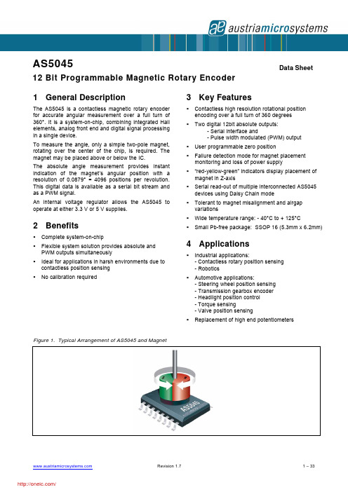
1 General DescriptionThe AS5045 is a contactless magnetic rotary encoder for accurate angular measurement over a full turn of 360°. It is a system-on-chip, combining integrated Hall elements, analog front end and digital signal processing in a single device.To measure the angle, only a simple two-pole magnet, rotating over the center of the chip, is required. The magnet may be placed above or below the IC.The absolute angle measurement provides instant indication of the magnet’s angular position with a resolution of 0.0879° = 4096 positions per revolution. This digital data is available as a serial bit stream and as a PWM signal.An internal voltage regulator allows the AS5045 to operate at either 3.3 V or 5 V supplies.2 BenefitsComplete system-on-chipFlexible system solution provides absolute andPWM outputs simultaneously Ideal for applications in harsh environments due tocontactless position sensing No calibration required3 Key FeaturesContactless high resolution rotational positionencoding over a full turn of 360 degrees Two digital 12bit absolute outputs:- Serial interface and- Pulse width modulated (PWM) output User programmable zero positionFailure detection mode for magnet placementmonitoring and loss of power supply “red-yellow-green” indicators display placement ofmagnet in Z-axis Serial read-out of multiple interconnected AS5045devices using Daisy Chain mode Tolerant to magnet misalignment and airgapvariations Wide temperature range: - 40°C to + 125°CSmall Pb-free package: SSOP 16 (5.3mm x 6.2mm)4 ApplicationsIndustrial applications:- Contactless rotary position sensing - Robotics Automotive applications:- Steering wheel position sensing - Transmission gearbox encoder - Headlight position control - Torque sensing- Valve position sensing Replacement of high end potentiometersFigure 1. Typical Arrangement of AS5045 and MagnetAS504512 Bit Programmable Magnetic Rotary Encoder Data SheetTable of Contents1General Description (1)2Benefits (1)3Key Features (1)4Applications (1)5Pinout (4)5.1Pin Configuration (4)5.2Pin Description (4)6Electrical Characteristics (5)6.1AS5045 Differences to AS5040 (5)6.2Absolute Maximum Ratings (non operating) (6)6.3Operating Conditions (6)6.4DC Characteristics for Digital Inputs and Outputs (7)6.4.1CMOS Schmitt-Trigger Inputs: CLK, CSn. (CSn = internal Pull-up) (7)6.4.2CMOS / Program Input: Prog (7)6.4.3CMOS Output Open Drain: MagINCn, MagDECn (7)6.4.4CMOS Output: PWM (7)6.4.5Tristate CMOS Output: DO (8)6.5Magnetic Input Specification (8)6.6Electrical System Specifications (9)6.7Timing Characteristics (10)6.7.1Synchronous Serial Interface (SSI) (10)6.7.2Pulse Width Modulation Output (11)6.8Programming Conditions (11)7Functional Description (12)8Mode Input Pin (13)8.1Synchronous Serial Interface (SSI) (13)8.1.1Data Content (14)8.1.2Z-axis Range Indication (Push Button Feature, Red/Yellow/Green Indicator) (14)8.2Daisy Chain Mode (15)9Pulse Width Modulation (PWM) Output (16)9.1Changing the PWM Frequency (17)10Analog Output (17)11Programming the AS5045 (18)11.1Zero Position Programming (18)11.2Repeated OTP Programming (18)11.3Non-permanent Programming (19)11.4Analog Readback Mode (20)12Alignment Mode (21)13 3.3V / 5V Operation (22)14Choosing the Proper Magnet (23)14.1Physical Placement of the Magnet (24)15Simulation Modeling (25)16Failure Diagnostics (26)16.1Magnetic Field Strength Diagnosis (26)16.2Power Supply Failure Detection (26)17Angular Output Tolerances (26)17.1Accuracy (26)17.2Transition Noise (28)17.3High Speed Operation (28)17.3.1Sampling Rate (28)17.4Propagation Delays (29)17.4.1Angular Error Caused by Propagation Delay (29)17.5Internal Timing Tolerance (29)17.6Temperature (30)17.6.1Magnetic Temperature Coefficient (30)17.7Accuracy over Temperature (30)17.7.1Timing Tolerance over Temperature (30)18Package Drawings and Markings (31)19Ordering Information (31)20Recommended PCB Footprint (32)5 Pinout5.1 Pin ConfigurationFigure 2. Pin Configuration SSOP165.2 Pin DescriptionTable 1 shows the description of each pin of the standard SSOP16 package (Shrink Small Outline Package, 16 leads, body size: 5.3mm x 6.2mmm; see Figure 2).Pins 7, 15 and 16 supply pins, pins 3, 4, 5, 6, 13 and 14 are for internal use and must not be connected.Pins 1 and 2 MagINCn and MagDECn are the magnetic field change indicators (magnetic field strength increase or decrease through variation of the distance between the magnet and the device). These outputs can be used to detect the valid magnetic field range. Furthermore those indicators can also be used for contact-less push-button functionality.Pin 6 Mode allows switching between filtered (slow) and unfiltered (fast mode). This pin must be tied to VSS or VDD5V, and must not be switched after power up. See chapter 8 Mode Input Pin.Pin 8 Prog is used to program the zero-position into the OTP (see chapter 11.1 Zero Position Programming).This pin is also used as digital input to shift serial data through the device in Daisy Chain configuration, (see chapter 8.2 Daisy Chain Mode).Pin 11 Chip Select (CSn; active low) selects a device within a network of AS5045 encoders and initiates serial data transfer. A logic high at CSn puts the data output pin (DO) to tri-state and terminates serial data transfer. This pin is also used for alignment mode (Figure 14) and programming mode (Figure 10).Pin 12 PWM allows a single wire output of the 10-bit absolute position value. The value is encoded into a pulse width modulated signal with 1µs pulse width per step (1µs to 4096µs over a full turn). By using an external low pass filter, the digital PWM signal is converted into an analog voltage, making a direct replacement of potentiometers possible.Table 1. Pin DescriptionPin Symbol Type Description1MagINCn DO_OD Magnet Field Mag nitude INC rease; active low, indicates a distance reduction between the magnet and the device surface. See Table 52MagDECn DO_OD Magnet Field Mag nitude DEC rease; active low, indicates a distance increase between the device and the magnet. See Table 53 NC - Must be left unconnected4 NC - Must be left unconnectedPin Symbol Type Description 5 NC - Must be left unconnected6Mode - Select between slow (low, VSS) and fast (high, VDD5V) mode. Internal pull-down resistor.7 VSS S Negative Supply Voltage (GND)8Prog_DI DI_PD OTP Prog ramming Input and Data Input for Daisy Chain mode. Internal pull-down resistor (~74kΩ). Connect to VSS if not used9 DO DO_TD ata O utput of Synchronous Serial Interface10 CLK DI,ST Cl oc k Input of Synchronous Serial Interface; Schmitt-Trigger input11 CSn DI_PU,STC hip S elect, active low; Schmitt-Trigger input, internal pull-up resistor (~50kΩ)12 PWM DO P ulse W idth M odulation of approx. 244Hz; 1µs/step (opt. 122Hz; 2µs/step)13 NC - Must be left unconnected14 NC - Must be left unconnected15VDD3V3 S 3V-Regulator Output, internally regulated from VDD5V. Connect to VDD5V for 3V supply voltage. Do not load externally.16 VDD5V S Positive Supply Voltage, 3.0 to 5.5 VDO_OD digital output open drain S supply pinDO digital output DI digital inputDI_PD digital input pull-down DO_T digital output /tri-stateDI_PU digital input pull-up ST Schmitt-Trigger input6 Electrical Characteristics6.1 AS5045 Differences to AS5040All parameters are according to AS5040 datasheet except for the parameters shown below: Building Block AS5045 AS5040Resolution 12bits, 0.088°/step. 10bit, 0.35°/stepData length Read: 18bits(12bits data + 6 bits status)OTP write: 18 bits(12bits zero position + 6 bits mode selection) Read: 16bits(10bits data + 6 bits status)OTP write: 16 bits(10bits zero position + 6 bits mode selection)Incremental encoder Not usedPin 3: not usedPin 4:not usedQuadrature, step/direction and BLDC motorcommutation modesPin 3:incremental output A_LSB_UPin 4:incremental output B_DIR_VPins 1 and 2 MagINCn, MagDECn: same feature asAS5040, additional OTP option for red-yellow-green magnetic range MagINCn, MagDECn indicate in-range or out-of-range magnetic field plus movement of magnet in z-axisPin 6 MODE pin, switch between fast and slowmodePin 6:Index outputPin 12 PWM output: frequency selectable by OTP:1µs / step, 4096 steps per revolution,f=244Hz 2µs/ step, 4096 steps perrevolution, f=122Hz PWM output:1µs / step, 1024 steps per revolution, 976Hz PWM frequencySampling frequency Selectable by MODE input pin:2.5kHz, 10kHzFixed at 10kHz @10bit resolutionBuilding Block AS5045AS5040 Propagation delay 384µs (slow mode) 96µs (fast mode)48µs Transition noise (rms; 1sigma) 0.03 degrees max. (slow mode) 0.06 degrees max. (fast mode)0.12 degreesOTP programming options Zero position, rotational direction, PWMdisable, 2 Magnetic Field indicator modes, 2 PWM frequenciesZero position, rotational direction, incremental modes, index bit width6.2 Absolute Maximum Ratings (non operating)Stresses beyond those listed under “Absolute Maximum Ratings“ may cause permanent damage to the device. These are stress ratings only. Functional operation of the device at these or any other conditions beyond those indicated under “Operating Conditions” is not implied. Exposure to absolute maximum rating conditions for extended periods may affect device reliability. ParameterSymbol Min Max Unit Note DC supply voltage at pin VDD5V VDD5V -0.3 7 V DC supply voltage at pin VDD3V3 VDD3V35VInput pin voltageV in -0.3VDD5V+0.3 V Except VDD3V3 Input current (latchup immunity) I scr -100 100 mA Norm: JEDEC 78Electrostatic discharge ESD ± 2 kV Norm: MIL 883 E method 3015 Storage temperature T strg-55125°CMin – 67°F ; Max +257°FBody temperature (Lead-free package)T Body 260°C t=20 to 40s,Norm: IPC/JEDEC J-Std-020 Lead finish 100% Sn “matte tin” Humidity non-condensing H585%6.3 Operating ConditionsParameterSymbol Min Typ Max UnitNoteAmbient temperature T amb -40125 °C -40°F…+257°FSupply currentI supp 1621 mA Supply voltage at pin VDD5V Voltage regulator output voltage at pin VDD3V3VDD5V VDD3V3 4.53.0 5.03.3 5.5 3.6 V 5V operationSupply voltage at pin VDD5V Supply voltage at pin VDD3V3 VDD5V VDD3V33.03.03.33.33.6 3.6V3.3V operation(pin VDD5V and VDD3V3 connected)6.4 DC Characteristics for Digital Inputs and Outputs6.4.1 CMOS Schmitt-Trigger Inputs: CLK, CSn. (CSn = internal Pull-up)(operating conditions: T amb = -40 to +125°C, VDD5V = 3.0-3.6V (3V operation) VDD5V = 4.5-5.5V (5V operation) unless otherwise noted) ParameterSymbol Min Max Unit NoteHigh level input voltage V IH 0.7 * VDD5VV Normal operation Low level input voltage V IL0.3 * VDD5VVSchmitt Trigger hysteresis V Ion- V Ioff 1V-1 1 CLK only Input leakage current Pull-up low level input current I LEAK I iL-30 -100µA µA CSn only, VDD5V: 5.0V6.4.2 CMOS / Program Input: Prog(operating conditions: T amb = -40 to +125°C, VDD5V = 3.0-3.6V (3V operation) VDD5V = 4.5-5.5V (5V operation)unless otherwise noted) ParameterSymbol Min Max Unit Note High level input voltage VIH 0.7 * VDD5VVDD5VVHigh level input voltage VPROG See Programming ConditionsV During programming Low level input voltage VIL 0.3 * VDD5VVHigh level input current IiL30100µAVDD5V: 5.5V6.4.3 CMOS Output Open Drain: MagINCn, MagDECn(operating conditions: T amb = -40 to +125°C, VDD5V = 3.0-3.6V (3V operation) VDD5V = 4.5-5.5V (5V operation)unless otherwise noted) ParameterSymbolMinMax UnitNote Low level output voltage V OL VSS+0.4 V Output currentI O4 2mAVDD5V: 4.5V VDD5V: 3VOpen drain leakage current I OZ 1 µA6.4.4 CMOS Output: PWM(operating conditions: T amb = -40 to +125°C, VDD5V = 3.0-3.6V (3V operation) VDD5V = 4.5-5.5V (5V operation)unless otherwise noted) ParameterSymbolMinMax UnitNoteHigh level output voltage V OH VDD5V-0.5 V Low level output voltage V OL VSS+0.4 V Output current I O4 2mA mAVDD5V: 4.5V VDD5V: 3V6.4.5 Tristate CMOS Output: DO(operating conditions: T amb = -40 to +125°C, VDD5V = 3.0-3.6V (3V operation) VDD5V = 4.5-5.5V (5V operation) unless otherwise noted) ParameterSymbolMinMax UnitNoteHigh level output voltage V OH VDD5V –0.5VLow level output voltage V OL VSS+0.4 VOutput currentI O4 2mAmAVDD5V: 4.5V VDD5V: 3VTri-state leakage current I OZ 1 µA6.5 Magnetic Input Specification(operating conditions: T amb = -40 to +125°C, VDD5V = 3.0-3.6V (3V operation) VDD5V = 4.5-5.5V (5V operation)unless otherwise noted)Two-pole cylindrical diametrically magnetised source: ParameterSymbolMinTypMaxUnitNoteDiameter d mag 4 6 mm Thickness t mag 2.5 mm Recommended magnet: Ø 6mm x 2.5mm forcylindrical magnets Magnetic input fieldamplitude B pk 4575 mTRequired vertical component of the magnetic field strength on the die’s surface, measured along a concentric circle with a radius of 1.1mm Magnetic offset B off ± 10mT Constant magnetic stray field Field non-linearity5 %Including offset gradient2.44146 rpm @ 4096 positions/rev.; fast modeInput frequency (rotational speed of magnet)f mag_abs0.61Hz36.6rpm @ 4096 positions/rev.; slow mode Displacement radiusDisp0.25mmMax. offset between defined device center and magnet axis (see Figure 18) Eccentricity Ecc 100µm Eccentricity of magnet center to rotational axis-0.12NdFeB (Neodymium Iron Boron) Recommended magnetmaterial andtemperature drift -0.035%/KSmCo (Samarium Cobalt)6.6 Electrical System Specifications(operating conditions: T amb = -40 to +125°C, VDD5V = 3.0~3.6V (3V operation) VDD5V = 4.5~5.5V (5V operation) unless otherwise noted) ParameterSymbolMinTypMaxUnitNoteResolution RES 12 bit 0.088 deg Integral non-linearity (optimum)INL opt± 0.5 deg Maximum error with respect to the best line fit. Centered magnet without calibration, T amb =25 °C. Integral non-linearity (optimum)INL temp± 0.9 degMaximum error with respect to the best line fit. Centered magnetwithout calibration, T amb = -40 to +125°CIntegral non-linearity INL ± 1.4 degBest line fit =(Err max – Err min ) / 2Over displacement tolerance with 6mm diameter magnet, without calibration,T amb = -40 to +125°C Differential non-linearity DNL ±0.044 deg 12bit, no missing codes 0.06 1 sigma, fast mode (MODE = 1)Transition noiseTN0.03deg RMS1 sigma, slow mode (MODE=0 or open)Power-on reset thresholds On voltage; 300mV typ. hysteresisOff voltage; 300mV typ. hysteresisV on V off 1.37 1.08 2.2 1.9 2.9 2.6VDC supply voltage 3.3V (VDD3V3)DC supply voltage 3.3V (VDD3V3)20Fast mode (Mode = 1); until status bit OCF = 1Power-up timet PwrUp80msSlow mode (Mode = 0 or open); until OCF = 196Fast mode (MODE=1)System propagation delay absolute output : delay of ADC, DSP and absolute interfacet delay384µsSlow mode (MODE=0 or open) 2.48 2.61 2.74T amb = 25°C, slow mode (MODE=0 or open)Internal sampling rate for absolute output:f S2.35 2.61 2.87 kHzT amb = -40 to +125°C, slow mode (MODE=0 or open) 9.90 10.42 10.94T amb = 25°C, fast mode (MODE = 1)Internal sampling rate forabsolute outputf S9.38 10.42 11.46kHz T amb = -40 to +125°C, : fast mode (MODE = 1)Read-out frequency CLK1MHz Max. clock frequency to read out serial dataFigure 3. Integral and Differential Non-linearity (example)Integral Non-Linearity (INL) is the maximum deviation between actual position and indicated position. Differential Non-Linearity (DNL) is the maximum deviation of the step length from one position to the next. Transition Noise (TN) is the repeatability of an indicated position6.7 Timing Characteristics6.7.1Synchronous Serial Interface (SSI)(operating conditions: T amb = -40 to +125°C, VDD5V = 3.0~3.6V (3V operation) VDD5V = 4.5~5.5V (5V operation) unless otherwise noted) ParameterSymbol MinTypMaxUnitNoteData output activated (logic high)t DO active 100 nsTime between falling edge of CSn and dataoutput activated First data shifted to output registert CLK FE500 nsTime between falling edge of CSn and firstfalling edge of CLKStart of data output T CLK / 2 500nsRising edge of CLK shifts out one bit at a timeData output valid t DO valid357 375 394 nsTime between rising edge of CLK and dataoutput validData output tristate t DO tristate100 nsAfter the last bit DO changes back to“tristate”Pulse width of CSn t CSn 500ns CSn = high; To initiate read-out of next angular position Read-out frequencyf CLK>01MHzClock frequency to read out serial data分销商库存信息:AMSAS5045-ASST AS5045-ASSU AS5045 PB AS5045 DB V2AS5045 AB。

基于单总线技术的分布式环境监控系统硬件设计白明;赵鑫【摘要】介绍了一个基于1-Wire总线网络的分布式温湿度监控系统的硬件设计.他由主控机和以单片机为核心的从机组成.由于采用1-Wire总线技术,该系统硬件接口比传统的设备更简单可靠,具有网络化的温湿度感知、能实现分布式测量温度湿度,并具有在异常环境条件下告警的功能;经实际调试证明,该系统安装简便、可扩展性能好、性价比高,对其他环境监控系统的设计具有一定的参考作用.【期刊名称】《现代电子技术》【年(卷),期】2006(029)017【总页数】3页(P106-108)【关键词】1-Wire网络;温湿度监控;单片机;AT89C52【作者】白明;赵鑫【作者单位】空军工程大学,工程学院,陕西,西安,710038;空军工程大学,工程学院,陕西,西安,710038【正文语种】中文【中图分类】TN41;TP331 引言在仓库管理、图书保存和工业测量等工作过程中,环境条件中的温湿度指标是需要实时监测的重要参数;实现对温度和湿度的监控具有十分重大的意义。
但目前常用的许多温湿度实时测控装置往往单站化、布线施工麻烦、可扩展性不强,并且不能实现智能化。
为了克服这些缺点,本文设计了一种基于1-Wire网络的分布式环境监测系统。
该系统可实现的功能如下:(1) 在微型局域网(Micro LAN)内可以实现远程数据采集和远程数据查询;(2) 扩展性能好,添加一个温度或湿度模块后,主控机能够自动搜索;(3) 测量精度指标高:测温精度为0.5℃,测湿精度为3%RH;(4) 可实时测量环境温度、湿度的变化情况;(5) 网络化的温湿度感知,实现多点测温、湿度。
(6) 具有环境条件异常告警模块,方便设备操作和仪器管理;(7) 成本低,通过双绞线进行通讯。
(8) 安装简便,维护方便、可靠性高。
2 1-Wire网络及其工作原理美国达拉斯半导体公司(Dallas Semiconductor)推出的单总线(1-Wire)是一种简单的信号交换方式,他在主机与外围器件之间通过一条线路进行双向通信。