Spartan-6datasheetSpartan系列FPGA芯片
- 格式:pdf
- 大小:1.86 MB
- 文档页数:89
Spartan-6 FPGA Electrical CharacteristicsSpartan®-6 LX and LXT FPGAs are available in various speed grades, with -3 having the highest performance. The DC and AC electrical parameters of the Automotive XA Spartan-6 FPGAs and Defense-grade Spartan-6Q FPGAs devices are equivalent to the commercial specifications except where noted. The timing characteristics of the commercial (XC) -2 speed grade industrial device are the same as for a -2 speed grade commercial device. The -2Q and -3Q speed grades areexclusively for the expanded (Q) temperature range. The timing characteristics are equivalent to those shown for the -2 and -3 speed grades for the Automotive and Defense-grade devices.Spartan-6FPGA DC and AC characteristics are specified for commercial (C), industrial (I), and expanded (Q) temperature ranges. Only selected speed grades and/or devices might be available in the industrial or expanded temperature ranges for Automotive and Defense-grade devices. References to device names refer to all available variations of that part number (for example, LX75 could denote XC6SLX75, XA6SLX75, or XQ6SLX75). The Spartan-6 FPGA -3N speed grade designates devices that do not support MCB functionality.All supply voltage and junction temperature specifications are representative of worst-case conditions. The parameters included are common to popular designs and typical applications. Available device and package combinations can be found at:DS162 (v3.1.1) January 30, 2015Product Specification找FPGA,上赛灵思半导体(深圳)有限公司V IN and V TS (3)I/O input voltage or voltage applied to 3-state output, relative to GND (4)All user and dedicatedI/OsCommercialDC–0.60 to 4.10V 20% overshoot duration –0.75 to 4.25V 8% overshoot duration (5)–0.75 to 4.40V IndustrialDC–0.60 to 3.95V 20% overshoot duration –0.75 to 4.15V 4% overshoot duration (5)–0.75 to 4.40V Expanded (Q)DC–0.60 to 3.95V 20% overshoot duration–0.75 to 4.15V 4% overshoot duration (5)–0.75 to 4.40V Restricted tomaximum of 100 user I/OsCommercial20% overshoot duration –0.75 to 4.35V 15% overshoot duration (5)–0.75 to 4.40V 10% overshoot duration–0.75 to 4.45V Industrial 20% overshoot duration –0.75 to 4.25V 10% overshoot duration –0.75 to 4.35V 8% overshoot duration (5)–0.75 to 4.40V Expanded (Q)20% overshoot duration–0.75 to 4.25V 10% overshoot duration–0.75 to 4.35V 8% overshoot duration (5)–0.75 to 4.40V T STGStorage temperature (ambient)–65to 150°C T SOLMaximum soldering temperature (6)(TQG144, CPG196, CSG225, CSG324, CSG484, and FTG256)+260°C Maximum soldering temperature (6) (Pb-free packages: FGG484, FGG676, and FGG900)+250°C Maximum soldering temperature (6) (Pb packages: CS484, FT256, FG484, FG676, and FG900)+220°C T jMaximum junction temperature (6)+125°CNotes:1.Stresses beyond those listed under Absolute Maximum Ratings might cause permanent damage to the device. These are stress ratings only, and functional operation of the device at these or any other conditions beyond those listed under Operating Conditions is not implied.Exposure to Absolute Maximum Ratings conditions for extended periods of time might affect device reliability.2.When programming eFUSE, V FS ≤V CCAUX . Requires up to 40mA current. For read mode, V FS can be between GND and3.45V .3.I/O absolute maximum limit applied to DC and AC signals. Overshoot duration is the percentage of a data period that the I/O is stressed beyond 3.45V .4.For I/O operation, refer to UG381: Spartan-6 FPGA SelectIO Resources User Guide .5.Maximum percent overshoot duration to meet 4.40V maximum.6.T SOL is the maximum soldering temperature for component bodies. For soldering guidelines and thermal considerations,see UG385: Spartan-6 FPGA Packaging and Pinout Specification .Table 1:Absolute Maximum Ratings (1) (Cont’d)SymbolDescriptionUnitseFUSE Read EnduranceTable11 lists the minimum guaranteed number of read cycle operations for Device DNA and for the AES eFUSE key. For more information, see UG380: Spartan-6 FPGA Configuration User Guide.Table 11:eFUSE Read EnduranceSymbol DescriptionSpeed Grade Units(Min) -3-3N-2-1LDNA_CYCLES Number of DNA_PORT READ operations or JT AG ISC_DNA read command operations. Unaffected by SHIFT operations.30,000,000ReadCyclesAES_CYCLES Number of JTAG FUSE_KEY or FUSE_CNTL read command operations.Unaffected by SHIFT operations.30,000,000ReadCyclesSymbol Description Typ(1)Max UnitsI MGTAVCC GTP transceiver internal analog supply current40.4Note2mAI MGTAVTTTX GTP transmitter termination supply current27.4mA I MGTAVTTRX GTP receiver termination supply current13.6mA I MGTAVCCPLL GTP transmitter and receiver PLL supply current28.7mA R MGTRREF Precision reference resistor for internal calibration termination50.0 ±1%toleranceΩGTP Transceiver DC Input and Output LevelsTable 16 summarizes the DC output specifications of the GTP transceivers in Spartan-6 FPGAs. Figure 1 shows the single-ended output voltage swing. Figure 2 shows the peak-to-peak differential output voltage.Consult UG386: Spartan-6 FPGA GTP Transceivers User Guide for further details.Table 17 summarizes the DC specifications of the clock input of the GTP transceiver. Consult UG386: Spartan-6 FPGA GTP Transceivers User Guide for further details.Table 16:GTP Transceiver DC SpecificationsSymbol DC ParameterConditionsMin Typ Max Units DV PPIN Differential peak-to-peak input voltageExternal AC coupled 140–2000mV V IN Absolute input voltage DC coupledMGT AVTTRX =1.2V –400–MGTAVTTRXmV V CMIN Common mode input voltageDC coupledMGTAVTTRX =1.2V–3/4MGTAVTTRX–mV DV PPOUT Differential peak-to-peak output voltage (1)T ransmitter output swing is set to maximum setting 1000––mV V SEOUT Single-ended output voltage swing (1)––500mV V CMOUTDCCommon mode output voltage Equation basedMGTAVTTTX –V SEOUT /2mV R IN Differential input resistance 80100130ΩR OUT Differential output resistance 80100130ΩT OSKEW Transmitter output skew––15ps C EXTRecommended external AC coupling capacitor (2)75100200nFNotes:1.The output swing and preemphasis levels are programmable using the attributes discussed in UG386: Spartan-6 FPGA GTP T ransceivers UserGuide and can result in values lower than reported in this table. DV PPOUT is the minimum guaranteed value at the maximum setting. Refer to UG386:Spartan-6 FPGA GTP Transceivers User Guide for nominal values.2.Other values can be used as appropriate to conform to specific protocols and standards.Figure 1:Single-Ended Peak-to-Peak VoltageFigure 2:Differential Peak-to-Peak Voltage。
Spartan6系列之器件引脚功能详述由技术编辑于星期四, 09/25/2014 - 14:48 发表1. Spartan-6系列封装概述Spartan-6系列具有低成本、省空间的封装形式,能使用户引脚密度最大化。
所有Spartan-6 LX器件之间的引脚分配是兼容的,所有Spartan-6 LXT器件之间的引脚分配是兼容的,但是Spartan-6 LX和Spartan-6 LXT器件之间的引脚分配是不兼容的。
表格 1Spartan-6系列FPGA封装2. Spartan-6系列引脚分配及功能详述Spartan-6系列有自己的专用引脚,这些引脚是不能作为Select IO使用的,这些专用引脚包括:专用配置引脚,表格2所示,GTP高速串行收发器引脚,表格3所示表格 2Spartan-6 FPGA专用配置引脚注意:只有LX75, LX75T, LX100, LX100T, LX150, and LX150T器件才有VFS、VBATT、RFUSE引脚。
表格 3Spartan-6器件GTP通道数目注意:LX75T在FG(G)484 和 CS(G)484中封装4个GTP通道,而在FG(G)676中封装了8个GTP通道;LX100T在FG(G)484 和 CS(G)484中封装4个GTP通道,而在FG(G)676 和 FG(G)900中封装了8个GTP通道。
如表4,每一种型号、每一种封装的器件的可用IO引脚数目不尽相同,例如对于LX4 TQG144器件,它总共有引脚144个,其中可作为单端IO引脚使用的IO个数为102个,这102个单端引脚可作为51对差分IO使用,另外的32个引脚为电源或特殊功能如配置引脚。
表格 4Spartan6系列各型号封装可用的IO资源汇总表格 5引脚功能详述3. Spartan-6系列GTP Transceiver引脚如表6所示,对LX25T,LX45T而言,只有一个GTP Transceiver通道,它的位置是X0Y0,所再Bank号为101;其他信号GTP Transceiver的解释类似。
SP601 Hardware User GuideUG518 (v1.7) September 26, 2012© Copyright 2009–2012 Xilinx, Inc. Xilinx, the Xilinx logo, Artix, ISE, Kintex, Spartan, Virtex, Zynq, and other designated brands included herein are trademarks of Xilinx in the United States and other countries. All other trademarks are the property of their respective owners. DISCLAIMERThe information disclosed to you hereunder (the “Materials”) is provided solely for the selection and use of Xilinx products. To the maximum extent permitted by applicable law: (1) Materials are made available “AS IS” and with all faults, Xilinx hereby DISCLAIMS ALL WARRANTIES AND CONDITIONS, EXPRESS, IMPLIED, OR ST ATUTORY, INCLUDING BUT NOT LIMITED TO WARRANTIES OF MERCHANTABILITY, NON-INFRINGEMENT, OR FITNESS FOR ANY PARTICULAR PURPOSE; and (2) Xilinx shall not be liable (whether in contract or tort, including negligence, or under any other theory of liability) for any loss or damage of any kind or nature related to, arising under, or in connection with, the Materials (including your use of the Materials), including for any direct, indirect, special, incidental, or consequential loss or damage (including loss of data, profits, goodwill, or any type of loss or damage suffered as a result of any action brought by a third party) even if such damage or loss was reasonably foreseeable or Xilinx had been advised of the possibility of the same. Xilinx assumes no obligation to correct any errors contained in the Materials, or to advise you of any corrections or update. Y ou may not reproduce, modify, distribute, or publicly display the Materials without prior written consent. Certain products are subject to the terms and conditions of the Limited Warranties which can be viewed at /warranty.htm; IP cores may be subject to warranty and support terms contained in a license issued to you by Xilinx. Xilinx products are not designed or intended to be fail-safe or for use in any application requiring fail-safe performance; you assume sole risk and liability for use of Xilinx products in Critical Applications:/warranty.htm#critapps.Revision HistoryThe following table shows the revision history for this document.Date Version Revision07/15/09 1.0Initial Xilinx release.08/19/09 1.1•Added Appendix B, VITA 57.1 FMC LPC Connector Pinout.•Updated Figure1-17.•Updated Table1-4, Table1-19, and Table1-22.•Added introductory paragraph to Appendix C, SP601 Master UCF.•Miscellaneous typographical edits and new user guide template.05/17/10 1.2•Updated Figure1-1, Figure1-2, Figure1-14, Figure1-18, Table1-9, Table1-1,Table1-11, and Table1-16.•Added Figure1-7, Figure1-8, and Table1-13.•Updated 9. VITA 57.1 FMC-LPC Connector, page25, Appendix B, VITA 57.1 FMCLPC Connector Pinout, and Appendix C, SP601 Master UCF.06/16/10 1.3Reversed order of 15. Configuration Options and 16. Power Management. Updated 1.Spartan-6 XC6SLX16-2CSG324 FPGA and 2. 128 MB DDR2 Component Memory. AddedTable1-26. Added UG394, Spartan-6 FPGA Power Management User Guide to Appendix D,References.09/24/10 1.4Added Power System Test Points, including Table1-25.02/16/11 1.5Added note and revised header description to indicate the I/Os support LVCMOS25signaling on page34. Revised oscillator manufacturer information from Epson to SiTimeon page page23 and page51.07/18/11 1.6Corrected wording from “PPM frequency jitter” to “PPM frequency stability” in sectionOscillator (Differential), page23. Added Table1-15, page27.09/26/12 1.7Added Regulatory and Compliance Information, page53.SP601 Hardware User Guide UG518 (v1.7) September 26, 2012SP601 Hardware User Guide 3UG518 (v1.7) September 26, 2012Revision History . . . . . . . . . . . . . . . . . . . . . . . . . . . . . . . . . . . . . . . . . . . . . . . . . . . . . . . . . . . . . 2Preface: About This GuideGuide Contents . . . . . . . . . . . . . . . . . . . . . . . . . . . . . . . . . . . . . . . . . . . . . . . . . . . . . . . . . . . . . . 5Additional Documentation . . . . . . . . . . . . . . . . . . . . . . . . . . . . . . . . . . . . . . . . . . . . . . . . . . . 5Additional Support Resources . . . . . . . . . . . . . . . . . . . . . . . . . . . . . . . . . . . . . . . . . . . . . . . . 6Chapter 1: SP601 Evaluation BoardOverview . . . . . . . . . . . . . . . . . . . . . . . . . . . . . . . . . . . . . . . . . . . . . . . . . . . . . . . . . . . . . . . . . . . . 7Additional Information. . . . . . . . . . . . . . . . . . . . . . . . . . . . . . . . . . . . . . . . . . . . . . . . . . . . . 7Features . . . . . . . . . . . . . . . . . . . . . . . . . . . . . . . . . . . . . . . . . . . . . . . . . . . . . . . . . . . . . . . . . . 8Block Diagram . . . . . . . . . . . . . . . . . . . . . . . . . . . . . . . . . . . . . . . . . . . . . . . . . . . . . . . . . . . . 9Related Xilinx Documents . . . . . . . . . . . . . . . . . . . . . . . . . . . . . . . . . . . . . . . . . . . . . . . . . . . . 9Detailed Description . . . . . . . . . . . . . . . . . . . . . . . . . . . . . . . . . . . . . . . . . . . . . . . . . . . . . . . . 101. Spartan-6 XC6SLX16-2CSG324 FPGA. . . . . . . . . . . . . . . . . . . . . . . . . . . . . . . . . . . . . . 11Configuration . . . . . . . . . . . . . . . . . . . . . . . . . . . . . . . . . . . . . . . . . . . . . . . . . . . . . . . . . 11I/O Voltage Rails . . . . . . . . . . . . . . . . . . . . . . . . . . . . . . . . . . . . . . . . . . . . . . . . . . . . . . 122. 128 MB DDR2 Component Memory . . . . . . . . . . . . . . . . . . . . . . . . . . . . . . . . . . . . . . . 123. SPI x4 Flash . . . . . . . . . . . . . . . . . . . . . . . . . . . . . . . . . . . . . . . . . . . . . . . . . . . . . . . . . . . . 154. Linear Flash BPI . . . . . . . . . . . . . . . . . . . . . . . . . . . . . . . . . . . . . . . . . . . . . . . . . . . . . . . . 175. 10/100/1000 Tri-Speed Ethernet PHY . . . . . . . . . . . . . . . . . . . . . . . . . . . . . . . . . . . . . 196. USB-to-UART Bridge. . . . . . . . . . . . . . . . . . . . . . . . . . . . . . . . . . . . . . . . . . . . . . . . . . . . 217. IIC Bus . . . . . . . . . . . . . . . . . . . . . . . . . . . . . . . . . . . . . . . . . . . . . . . . . . . . . . . . . . . . . . . . 228-Kb NV Memory . . . . . . . . . . . . . . . . . . . . . . . . . . . . . . . . . . . . . . . . . . . . . . . . . . . . . . 228. Clock Generation . . . . . . . . . . . . . . . . . . . . . . . . . . . . . . . . . . . . . . . . . . . . . . . . . . . . . . . 23Oscillator (Differential). . . . . . . . . . . . . . . . . . . . . . . . . . . . . . . . . . . . . . . . . . . . . . . . . . 23Oscillator Socket (Single-Ended, 2.5V or 3.3V) . . . . . . . . . . . . . . . . . . . . . . . . . . . . . . . . 24SMA Connectors (Differential). . . . . . . . . . . . . . . . . . . . . . . . . . . . . . . . . . . . . . . . . . . . 249. VITA 57.1 FMC-LPC Connector . . . . . . . . . . . . . . . . . . . . . . . . . . . . . . . . . . . . . . . . . . 2510. Status LEDs. . . . . . . . . . . . . . . . . . . . . . . . . . . . . . . . . . . . . . . . . . . . . . . . . . . . . . . . . . . 2811. FPGA Awake LED and Suspend Jumper. . . . . . . . . . . . . . . . . . . . . . . . . . . . . . . . . . 2912. FPGA INIT and DONE LEDs. . . . . . . . . . . . . . . . . . . . . . . . . . . . . . . . . . . . . . . . . . . . 3013. User I/O . . . . . . . . . . . . . . . . . . . . . . . . . . . . . . . . . . . . . . . . . . . . . . . . . . . . . . . . . . . . . 3114. FPGA_PROG_B Pushbutton Switch . . . . . . . . . . . . . . . . . . . . . . . . . . . . . . . . . . . . . . 3515. Configuration Options . . . . . . . . . . . . . . . . . . . . . . . . . . . . . . . . . . . . . . . . . . . . . . . . . 36JTAG Configuration . . . . . . . . . . . . . . . . . . . . . . . . . . . . . . . . . . . . . . . . . . . . . . . . . . . . 3616. Power Management. . . . . . . . . . . . . . . . . . . . . . . . . . . . . . . . . . . . . . . . . . . . . . . . . . . . 37AC Adapter and 5V Input Power Jack/Switch . . . . . . . . . . . . . . . . . . . . . . . . . . . . . . . . 37Onboard Power Supplies . . . . . . . . . . . . . . . . . . . . . . . . . . . . . . . . . . . . . . . . . . . . . . . . 37Power System Test Points . . . . . . . . . . . . . . . . . . . . . . . . . . . . . . . . . . . . . . . . . . . . . . . . 38Table of ContentsAppendix A: Default Jumper and Switch SettingsAppendix B: VITA 57.1 FMC LPC Connector PinoutAppendix C: SP601 Master UCFAppendix D: ReferencesAppendix E: Regulatory and Compliance InformationDirectives. . . . . . . . . . . . . . . . . . . . . . . . . . . . . . . . . . . . . . . . . . . . . . . . . . . . . . . . . . . . . . . . . . . 53Standards. . . . . . . . . . . . . . . . . . . . . . . . . . . . . . . . . . . . . . . . . . . . . . . . . . . . . . . . . . . . . . . . . . . 53 Electromagnetic Compatibility . . . . . . . . . . . . . . . . . . . . . . . . . . . . . . . . . . . . . . . . . . . . . 53Safety . . . . . . . . . . . . . . . . . . . . . . . . . . . . . . . . . . . . . . . . . . . . . . . . . . . . . . . . . . . . . . . . . . . 53 Markings . . . . . . . . . . . . . . . . . . . . . . . . . . . . . . . . . . . . . . . . . . . . . . . . . . . . . . . . . . . . . . . . . . . 54 SP601 Hardware User GuideUG518 (v1.7) September 26, 2012SP601 Hardware User Guide 5UG518 (v1.7) September 26, 2012PrefaceAbout This GuideThis manual accompanies the Spartan®-6 FPGA SP601 Evaluation Board and contains information about the SP601 hardware and software tools.Guide ContentsThis manual contains the following chapters:•Chapter 1, SP601 Evaluation Board , provides an overview of the SP601 evaluation board and details the components and features of the SP601 board.•Appendix A, Default Jumper and Switch Settings .•Appendix B, VITA 57.1 FMC LPC Connector Pinout .•Appendix C, SP601 Master UCF .•Appendix D, References .Additional DocumentationThe following documents are available for download at /products/spartan6.•Spartan-6 Family OverviewThis overview outlines the features and product selection of the Spartan-6 family.•Spartan-6 FPGA Data Sheet: DC and Switching CharacteristicsThis data sheet contains the DC and switching characteristic specifications for the Spartan-6 family.•Spartan-6 FPGA Packaging and Pinout SpecificationsThis specification includes the tables for device/package combinations and maximum I/Os, pin definitions, pinout tables, pinout diagrams, mechanical drawings, and thermal specifications.•Spartan-6 FPGA Configuration User GuideThis all-encompassing configuration guide includes chapters on configuration interfaces (serial and parallel), multi-bitstream management, bitstream encryption, boundary-scan and JTAG configuration, and reconfiguration techniques.•Spartan-6 FPGA SelectIO Resources User GuideThis guide describes the SelectIO™ resources available in all Spartan-6 devices.•Spartan-6 FPG A Clocking Resources User GuidePreface:About This GuideThis guide describes the clocking resources available in all Spartan-6 devices,including the DCMs and PLLs.•Spartan-6 FPGA Block RAM Resources User GuideThis guide describes the Spartan-6 device block RAM capabilities.•Spartan-6 FPGA DSP48A1 Slice User GuideThis guide describes the architecture of the DSP48A1 slice in Spartan-6FPGAs andprovides configuration examples.•Spartan-6 FPGA Memory Controller User GuideThis guide describes the Spartan-6 FPGA memory controller block, a dedicatedembedded multi-port memory controller that greatly simplifies interfacingSpartan-6FPGAs to the most popular memory standards.•Spartan-6 FPGA PCB Designer’s GuideThis guide provides information on PCB design for Spartan-6 devices, with a focus onstrategies for making design decisions at the PCB and interface level.Additional Support ResourcesTo search the database of silicon and software questions and answers or to create atechnical support case in WebCase, see the Xilinx website at:/support. SP601 Hardware User GuideUG518 (v1.7) September 26, 2012Chapter1 SP601 Evaluation BoardOverviewThe SP601 board enables hardware and software developers to create or evaluate designstargeting the Spartan®-6 XC6SLX16-2CSG324 FPGA.The SP601 provides board features for evaluating the Spartan-6 family that are common tomost entry-level development environments. Some commonly used features include aDDR2 memory controller, a parallel linear flash, a tri-mode Ethernet PHY, general-purposeI/O (GPIO), and a UART. Additional functionality can be added through the VITA 57.1.1expansion connector. Features, page8 provides a general listing of the board features withdetails provided in Detailed Description, page10.Additional InformationAdditional information and support material is located at:•/sp601This information includes:•Current version of this user guide in PDF format•Example design files for demonstration of Spartan-6 FPGA features and technology•Demonstration hardware and software configuration files for the SP601 linear and SPImemory devices•Reference Design Files•Schematics in PDF format and DxDesigner schematic format•Bill of materials (BOM)•Printed-circuit board (PCB) layout in Allegro PCB format•Gerber files for the PCB (Many free or shareware Gerber file viewers are available onthe internet for viewing and printing these files.)•Additional documentation, errata, frequently asked questions, and the latest newsFor information about the Spartan-6 family of FPGA devices, including product highlights,data sheets, user guides, and application notes, see the Spartan-6 FPGA website at/support/documentation/spartan-6.htm.SP601 Hardware User Guide 7 UG518 (v1.7) September 26, 2012Chapter 1:SP601 Evaluation BoardFeaturesThe SP601 board provides the following features (see Figure1-2 and Table1-1):• 1. Spartan-6 XC6SLX16-2CSG324 FPGA• 2. 128 MB DDR2 Component Memory• 3. SPI x4 Flash• 4. Linear Flash BPI• 5. 10/100/1000 Tri-Speed Ethernet PHY•7. IIC Bus•8Kb NV memory•External access 2-pin header•VITA 57.1 FMC-LPC connector•8. Clock Generation•Oscillator (Differential)•Oscillator Socket (Single-Ended, 2.5V or 3.3V)•SMA Connectors (Differential)•9. VITA 57.1 FMC-LPC Connector•10. Status LEDs•FPGA_AWAKE•INIT•DONE•13. User I/O•User LEDs•User DIP switch•User pushbuttons•GPIO male pin header•14. FPGA_PROG_B Pushbutton Switch•15. Configuration Options• 3. SPI x4 Flash (both onboard and off-board)• 4. Linear Flash BPI•JTAG Configuration•16. Power Management•AC Adapter and 5V Input Power Jack/Switch•Onboard Power Supplies SP601 Hardware User GuideUG518 (v1.7) September 26, 2012Related Xilinx DocumentsBlock DiagramFigure1-1 shows a high-level block diagram of the SP601 and its peripherals.Figure 1-1:SP601 Features and BankingRelated Xilinx DocumentsPrior to using the SP601 Evaluation Board, users should be familiar with Xilinx resources.See the following locations for additional documentation on Xilinx tools and solutions:•ISE: /ise•Answer Browser: /support•Intellectual Property: /ipcenterSP601 Hardware User Guide 9 UG518 (v1.7) September 26, 2012SP601 Hardware User GuideUG518 (v1.7) September 26, 2012Chapter 1:SP601 Evaluation BoardDetailed DescriptionFigure 1-2 shows a board photo with numbered features corresponding to Table 1-1 and the section headings in this document.The numbered features in Figure 1-2 correlate to the features and notes listed in Table 1-1.Figure 1-2:SP601 Board PhotoUG518_02_09100912843126137115109141581316Table 1-1:SP601 FeaturesNumberFeatureNotesSchematic Page1 Spartan-6 FP G A XC6SLX16-2CS G 3242DDR2 Component Elpida EDE1116ACBG 1Gb DDR2SDRAM53SPI x4 Flash and Headers SPI select and External Headers 84Linear Flash BPIStrataFlash 8-bit (J3 device), 3 pins shared w/ SPI x481. Spartan-6 XC6SLX16-2CSG 324 FPGAA Xilinx Spartan-6 XC6SLX16-2CSG324 FPGA is installed on the SP601 Evaluation Board.ReferencesSee the Spartan-6 FPGA Data Sheet . [Ref 1]ConfigurationThe SP601 supports configuration in the following modes:•Master SPI x4•Master SPI x4 with off-board device •BPI•JTAG (using the included USB-A to Mini-B cable)For details on configuring the FPGA, see 15. Configuration Options .The Mode DIP switch SW2 is set to M[1:0] = 01 Master SPI default.ReferencesSee the Spartan-6 FPGA Configuration User Guide for more information. [Ref 2]510/100/1000 Ethernet PHY GMII Marvell Alaska PHY76RS232 UART (USB Bridge)Uses CP2103 Serial-to-USB connection 107IICGoes to Header and VITA 57.1 FMC 108Clock, socket, SMA Differential, Single-Ended, Differential 99VITA 57.1 FMC-LPC connector LVDS signals, clocks, PRSNT 610LEDs Ethernet PHY Status711LED, Header FPGA Awake LED, Suspend Header 812LEDs FPGA INIT, DONE 913LED User I/O (active-High)9DIP SwitchUser I/O (active-High)9PushbuttonUser I/O, CPU_RESET (active-High)912-pin (8 I/O) Header6 pins x 2 male header with 8 I/Os (active-High)1014Pushbutton FPGA_PROG_B915USB JTAG Cypress USB to JTAG download cable logic14, 1516Onboard PowerPower Management11,12,13Table 1-1:SP601 Features (Cont’d)NumberFeatureNotesSchematic PageSP601 Hardware User Guide I/O Voltage RailsThere are four available banks on the LX16-CSG324 device. Banks 0, 1, and 2 are connected for 2.5V I/O. Bank 3 is used for the 1.8V DDR2 component memory interface of Spartan-6 FPGA’s hard memory controller. The voltage applied to the FPGA I/O banks used by the SP601 board is summarized in Table 1-2.ReferencesSee the Spartan-6 FPGA documentation for more information at /support/documentation/spartan-6.htm .2. 128 MB DDR2 Component MemoryThere are 128MB of DDR2 memory available on the SP601 board. A 1-Gb ElpidaEDE1116ACBG (84-ball) DDR2 memory component is accessible through Bank 3 of the LX16 device. The Spartan-6 FPGA hard memory controller is used for data transfer across the DDR2 memory interface’s 16-bit data path using SSTL18 signaling. The SP601 board supports the “standard” VCCINT setting of 1.20V ± 5%. This setting provides the standard memory controller block (MCB) performance of 625Mb/s for DDR2 memory in a -2 speed grade device. Signal integrity is maintained through DDR2 resistor terminations and memory on-die terminations (ODT), as shown in Table 1-3 and Table 1-4.Table 1-2:I/O Voltage Rail of FPGA BanksFPGA BankI/O Voltage Rail0 2.5V 1 2.5V 2 2.5V 31.8VTable 1-3:Termination Resistor RequirementsSignal NameBoard TerminationOn-Die TerminationDDR2_A[14:0]49.9Ω to V TT DDR2_BA[2:0]49.9Ω to V TT DDR2_RAS_N 49.9Ω to V TT DDR2_CAS_N 49.9Ω to V TT DDR2_WE_N 49.9Ω to V TT DDR2_CS_N 100Ω to GND DDR2_CKE 4.7K Ω to GND DDR2_ODT 4.7K Ω to GNDDDR2_DQ[15:0]ODT DDR2_UDQS[P ,N], DDR2_LDQS[P ,N]ODT DDR2_UDM, DDR2_LDMODTTable 1-5 shows the connections and pin numbers for the DDR2 Component Memory.DDR2_CK[P ,N]100Ω differential at memorycomponentNotes:1.Nominal value of V TT for DDR2 interface is 0.9V .Table 1-4:FPGA On-Chip (OCT) Termination External Resistor Requirements FPGA U1 PinFPGA Pin NumberBoard Connection for OCTZIO L6No Connect RZQC2100Ω to GROUNDTable 1-5:DDR2 Component Memory ConnectionsFPGA U1 PinSchematic Net Name Memory U2Pin NumberPin NameJ7DDR2_A0M8A0J6DDR2_A1M3A1H5DDR2_A2M7A2L7DDR2_A3N2A3F3DDR2_A4N8A4H4DDR2_A5N3A5H3DDR2_A6N7A6H6DDR2_A7P2A7D2DDR2_A8P8A8D1DDR2_A9P3A9F4DDR2_A10M2A10D3DDR2_A11P7A11G6DDR2_A12R2A12L2DDR2_DQ0G8DQ0L1DDR2_DQ1G2DQ1K2DDR2_DQ2H7DQ2K1DDR2_DQ3H3DQ3H2DDR2_DQ4H1DQ4H1DDR2_DQ5H9DQ5J3DDR2_DQ6F1DQ6Table 1-3:Termination Resistor Requirements (Cont’d)Signal NameBoard Termination On-Die TerminationSP601 Hardware User Guide ReferencesSee the Elpida DDR2 SDRAM Specifications for more information. [Ref 11]Also, see the Spartan-6 FPGA Memory Controller User Guide . [Ref 3]J1DDR2_DQ7F9DQ7M3DDR2_DQ8C8DQ8M1DDR2_DQ9C2DQ9N2DDR2_DQ10D7DQ10N1DDR2_DQ11D3DQ11T2DDR2_DQ12D1DQ12T1DDR2_DQ13D9DQ13U2DDR2_DQ14B1DQ14U1DDR2_DQ15B9DQ15F2DDR2_BA0L2BA0F1DDR2_BA1L3BA1E1DDR2_BA2L1BA2E3DDR2_WE_B K3WE L5DDR2_RAS_B K7RAS K5DDR2_CAS_B L7CAS K6DDR2_ODT K9ODT G3DDR2_CLK_P J8CK G1DDR2_CLK_N K8CK H7DDR2_CKE K2CKE L4DDR2_LDQS_P F7LDQS L3DDR2_LDQS_N E8LDQS P2DDR2_UDQS_P B7UDQS P1DDR2_UDQS_N A8UDQS K3DDR2_LDM F3LDM K4DDR2_UDMB3UDMTable 1-5:DDR2 Component Memory Connections (Cont’d)FPGA U1 PinSchematic Net Name Memory U2Pin NumberPin Name3. SPI x4 FlashThe Xilinx Spartan-6 FPGA hosts a SPI interface which is accessible to the Xilinx iMPACTconfiguration tool. The SPI memory device operates at 3.0V; the Spartan-6 FPGA I/Os are3.3V tolerant and provide electrically compatible logic levels to directly access the SPI flashthrough a 2.5V bank. The XC6SLX16-2CSG324 is a master device when accessing anexternal SPI flash memory device.The SP601 SPI interface has two parallel connected configuration options (see Figure1-4):an SPI X4 (Winbond W25Q64VSFIG) 64-Mb flash memory device and a flashprogramming header (J12). J12 supports a user-defined SPI mezzanine board. The SPIconfiguration source is selected via SPI select jumper J15. For details on configuring theFPGA, see 15. Configuration Options.Figure 1-3:J12 SPI Flash Programming HeaderSP601 Hardware User Guide ReferencesSee the Winbond Serial Flash Memory Data Sheet for more information. [Ref 12]See the XPS Serial Peripheral Interface Data Sheet for more information. [Ref 4]Figure 1-4:SPI Flash Interface TopologyTable 1-6:SPI x4 Memory ConnectionsFPGA U1 PinSchematic Net Name SPI MEM U17SPI HDR J12Pin #Pin NamePinNumberPin NameV2FPGA_PROG_B 1V14FPGA_D2_MISO31IO3_HOLD_B 2T14FPGA_D1_MISO2_R 9IO2_WP_B3V3SPI_CS_B4TMS T13FPGA_MOSI_CSI_B_MISO015DIN 5TDI R13FPGA_D0_DIN_MISO_MISO18IO1_DOUT6TDO R15FPGA_CCLK16CLK7TCK 8GND 9VCC3V3J15.2SPIX4_CS_B 7CS_B4. Linear Flash BPIAn 8-bit (16MB) Numonyx linear flash memory (TE28F128J3D-75) (J3D type) is used toprovide non-volatile bitstream, code, and data storage. The J3D devices operate at 3.0V; theSpartan-6 FPGA I/Os are 3.3V tolerant and provide electrically compatible logic levels todirectly access the linear flash BPI through a 2.5V bank. For details on configuring theFPGA, see 15. Configuration Options.Figure 1-5:Linear Flash BPI InterfaceTable 1-7:BPI Memory ConnectionsFPGA U1 Pin Schematic Net Name BPI Memory U10Pin Number Pin Name K18FLASH_A032A0K17FLASH_A128A1J18FLASH_A227A2J16FLASH_A326A3G18FLASH_A425A4G16FLASH_A524A5H16FLASH_A623A6H15FLASH_A722A7H14FLASH_A820A8H13FLASH_A919A9F18FLASH_A1018A10F17FLASH_A1117A11K13FLASH_A1213A12K12FLASH_A1312A13E18FLASH_A1411A14E16FLASH_A1510A15G13FLASH_A168A16SP601 Hardware User Guide Note:Memory U10 pin 56 address A24 is not connected on the 16 MB device. It is made availablefor larger density devices.ReferencesSee the Numonyx Embedded Flash Memory Data Sheet for more information. [Ref 13]In addition, see the Spartan-6 FPGA Configuration User Guide for more information. [Ref 2]H12FLASH_A177A17D18FLASH_A186A18D17FLASH_A195A19G14FLASH_A204A20F14FLASH_A213A21C18FLASH_A221A22C17FLASH_A2330A23F16FLASH_A2456A24R13FPGA_D0_DIN_MISO_MISO133DQ0T14FPGA_D1_MISO235DQ1V14FPGA_D2_MISO338DQ2U5FLASH_D340DQ3V5FLASH_D444DQ4R3FLASH_D546DQ5T3FLASH_D649DQ6R5FLASH_D751DQ7M16FLASH_WE_B 55WE_B L18FLASH_OE_B 54OE_B L17FLASH_CE_B14CE0B3FMC_PWR_GOOD_FLASH_RST_B16RP_BTable 1-7:BPI Memory Connections (Cont’d)FPGA U1 PinSchematic Net NameBPI Memory U10Pin NumberPin Name5. 10/100/1000 T ri-Speed Ethernet PHYThe SP601 uses the onboard Marvell Alaska PHY device (88E1111) for Ethernetcommunications at 10, 100, or 1000 Mb/s. The board supports a GMII/MII interface fromthe FPGA to the PHY. The PHY connection to a user-provided Ethernet cable is through aHalo HFJ11-1G01E RJ-45 connector with built-in magnetics.On power-up, or on reset, the PHY is configured to operate in GMII mode with PHYaddress 0b00111 using the settings shown in Table1-8. These settings can be overwrittenvia software commands passed over the MDIO interface.Table 1-8:PHY Configuration PinsPin Connection onBoardBit[2]Definition and ValueBit[1]Definition and ValueBit[0]Definition and ValueCFG0V CC 2.5V PHYADR[2] = 1PHYADR[1] = 1PHYADR[0] = 1 CFG1Ground ENA_PAUSE = 0PHYADR[4] = 0PHYADR[3] = 0 CFG2V CC 2.5V ANEG[3] = 1ANEG[2] = 1ANEG[1] = 1 CFG3V CC 2.5V ANEG[0] = 1ENA_XC = 1DIS_125 = 1 CFG4V CC 2.5V HWCFG_MD[2] = 1HWCFG_MD[1] = 1HWCFG_MD[0] = 1 CFG5V CC 2.5V DIS_FC = 1DIS_SLEEP = 1HWCFG_MD[3] = 1 CFG6PHY_LED_RX SEL_BDT = 0INT_POL = 175/50Ω = 0 Table 1-9:Ethernet PHY ConnectionsFPGA U1 Pin Schematic Net NameU3 M88E111Pin Number Pin NameP16PHY_MDIO33MDIO N14PHY_MDC35MDC J13PHY_INT32INT_B L13PHY_RESET36RESET_B M13PHY_CRS115CRS L14PHY_COL114COL L16PHY_RXCLK7RXCLK P17PHY_RXER8RXER N18PHY_RXCTL_RXDV4RXDV M14PHY_RXD03RXD0 U18PHY_RXD1128RXD1 U17PHY_RXD2126RXD2 T18PHY_RXD3125RXD3 T17PHY_RXD4124RXD4 N16PHY_RXD5123RXD5SP601 Hardware User GuideReferencesSee the Marvell Alaska Gigabit Ethernet Transceivers product page for more information.[Ref 16]Also, see the LogiCORE™ IP Tri-Mode Ethernet MAC User Guide . [Ref 5]N15PHY_RXD6121RXD6P18PHY_RXD7120RXD7A9 PHY_TXC_G TPCLK 14G TXCLKB9 PHY_TXCLK 10TXCLK A8 PHY_TXER 13TXER B8 PHY_TXCTL_TXEN 16TXEN F8 PHY_TXD018TXD0G 8 PHY_TXD119TXD1A6 PHY_TXD220TXD2B6 PHY_TXD324TXD3E6 PHY_TXD425TXD4F7 PHY_TXD526TXD5A5 PHY_TXD628TXD6C5 PHY_TXD729TXD7Table 1-9:Ethernet PHY Connections (Cont’d)FPGA U1 PinSchematic Net NameU3 M88E111Pin NumberPin Name6. USB-to-UART BridgeThe SP601 contains a Silicon Labs CP2103GM USB-to-UART bridge device (U4) which allows connection to a host computer with a USB cable. The USB cable is supplied in this evaluation kit (Type A end to host computer, Type Mini-B end to SP601 connector J9). Table 1-10 details the SP601 J9 pinout.Xilinx UART IP is expected to be implemented in the FPGA fabric. The FPGA supports the USB-to-UART bridge using four signal pins, transmit (TX), receive (RX), Request to Send (RTS), and Clear to Send (CTS).Silicon Labs provides royalty-free Virtual COM Port (VCP) drivers which permit the CP2103GM USB-to-UART bridge to appear as a COM port to host computercommunications application software (for example, HyperTerm or TeraTerm). The VCP device driver must be installed on the host PC prior to establishing communications with the SP601. Refer to the SP601 Getting Started Guide for driver installation instructions.ReferencesRefer to the Silicon Labs website for technical information on the CP2103GM and the VCP drivers.In addition, see some of the Xilinx UART IP specifications at:•/support/documentation/ip_documentation/xps_uartlite.pdf •/support/documentation/ip_documentation/xps_uart16550.pdfTable 1-10:USB Type B Pin Assignments and Signal DefinitionsUSB ConnectorPinSignal NameDescription1VBUS +5V from host system (not used)2USB_DATA_N Bidirectional differential serial data (N-side)3USB_DATA_P Bidirectional differential serial data (P-side)4GROUNDSignal groundTable 1-11:CP2103GM ConnectionsFPGA U1 PinUART Functionin FPGA Schematic Net Name U4 CP2103GMPinUART Function in CP2103GM U10RTS, output USB_1_CTS 22CTS, input T5CTS, input USB_1_RTS 23RTS, output L12TX, data out USB_1_RX 24RXD, data in K14RX, data inUSB_1_TX25TXD, data out。
Ompal138+Spartan-6FPGA核心板规格软硬件资料数据手册核心板简介创龙科技SOM-TL138F是一款基于TI OMAP-L138(定点/浮点DSP C674x + ARM9) + 紫光同创Logos/Xilinx Spartan-6低功耗FPGA处理器设计的工业级核心板。
核心板内部OMAP-L138与Logos/Spartan-6通过uPP、EMIFA、I2C通信总线连接,并通过工业级B2B连接器引出网口、EMIFA、SATA、USB、LCD等接口。
核心板经过专业的PCB Layout和高低温测试验证,稳定可靠,可满足各种工业应用环境。
用户使用核心板进行二次开发时,仅需专注上层运用,降低了开发难度和时间成本,可快速进行产品方案评估与技术预研。
图 1 核心板正面图图 2 核心板背面图图 3 核心板斜视图图 4 核心板侧视图典型应用领域•运动控制•电力设备•仪器仪表•医疗设备•通信探测•惯性导航软硬件参数硬件框图图 5 核心板硬件框图图 6 OMAP-L138资源框图图 7 Logos特性图 8 Spartan-6特性硬件参数表 1 OMAP-L138端硬件参数CPU CPU型号:TI OMAP-L1381x ARM9,主频456MHz1x DSP C674x,主频456MHz,支持浮点运算1x PRU-ICSS,含2个PRU(Programmable Real-time Unit)核心ROM512MByte NAND FLASH RAM128/256MByte DDR2LED 1x 电源指示灯2x 用户可编程指示灯B2B Connector 2x 80pin公座B2B连接器,2x 80pin母座B2B连接器,间距0.5mm,共320pin硬件资源1x VPIF Video OUT(支持SDTV和HDTV),ITU-BT.656 Format,ITU-BT.1120 and SMTPE296 Formats1x VPIF Video IN(支持SDTV,HDTV和Raw Capture Mode),ITU-BT.656 Format,ITU-BT.1120 and SMTPE296 Formats1x LCD Controller1x USB 1.1 HOST1x USB 2.0 OTG1x 10/100M Ethernet1x SATA2x MMC/SD/SDIO3x UART2x eHRPWM1x EMIFA,在核心板内部与FPGA通过普通IO连接3x eCAP2x I2C1x HPI1x uPP,在核心板内部与FPGA通过普通IO连接,可配置为1x 16bit或2x 8bit2x McBSP1x McASP2x SPI备注:B2B、电源、指示灯等部分硬件资源,OMAP-L138与FPGA共用。
XilinxFPGA引脚功能详细介绍注:技术交流用,希望对大家有所帮助。
IO_LXXY_# 用户IO引脚XX代表某个Bank内唯一的一对引脚,Y=[P|N]代表对上升沿还是下降沿敏感,#代表bank 号2.IO_LXXY_ZZZ_# 多功能引脚ZZZ代表在用户IO的基本上添加一个或多个以下功能。
Dn:I/O(在readback期间),在selectMAP或者BPI模式下,D[15:0]配置为数据口。
在从SelectMAP读反馈期间,如果RDWR_B=1,则这些引脚变成输出口。
配置完成后,这些引脚又作为普通用户引脚。
D0_DIN_MISO_MISO1:I,在并口模式(SelectMAP/BPI)下,D0是数据的最低位,在Bit-serial模式下,DIN是信号数据的输入;在SPI模式下,MISO是主输入或者从输出;在SPI*2或者SPI*4模式下,MISO1是SPI总线的第二位。
D1_MISO2,D2_MISO3:I,在并口模式下,D1和D2是数据总线的低位;在SPI*4模式下,MISO2和MISO3是SPI总线的MSBs。
An:O,A[25:0]为BPI模式的地址位。
配置完成后,变为用户I/O口。
AWAKE:O,电源保存挂起模式的状态输出引脚。
SUSPEND是一个专用引脚,AWAKE是一个多功能引脚。
除非SUSPEND模式被使能,AWAKE被用作用户I/O。
MOSI_CSI_B_MISO0:I/O,在SPI模式下,主输出或者从输入;在SelectMAP模式下,CSI_B是一个低电平有效的片选信号;在SPI*2或者SPI*4的模式下,MISO0是SPI总线的第一位数据。
FCS_B:O,BPI flash 的片选信号。
FOE_B:O,BPI flash的输出使能信号FWE_B:O,BPI flash 的写使用信号LDC:O,BPI模式配置期间为低电平HDC:O,BPI模式配置期间为高电平CSO_B:O,在并口模式下,工具链片选信号。
说明:I =Input, O=Output,I/O =Bidirec
设计注意提示
1.CPU外部晶振频率为24MHz。
2.核心板的I2C总线已用2.2K电阻上拉至
3.3V。
3.利用核心板进行设计底板时,请认真核对自己底板的核心板B2B连接器的信号引脚线序是否正确,连接样的B2B物料,可以联系我司采购。
4.有关信号详细功能,请查看芯片datasheet。
5.FPGA端管脚名中带前缀“n”的,在LX9/LX25/LX45中可能悬空
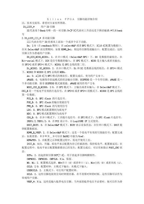
SOM-TLS6-A1核心板B2
directional,Z=Highimpedance, PWR=Supply voltage,GND=Ground
自己底板的核心板B2B连接器的信号引脚线序是否正确,连接器的摆放位置是否正确,请务必参考我司提供的底板PC 能悬空;具体请参考Xilinx用户指导文档:UG385
心板B2B信号列表
,请务必参考我司提供的底板PCB图进行核对。
核心板同
SOM-TLS6-A1核心板B2B信
B2B信号列表。
Spartan-6时钟管理模块的介绍与使用同步时序电路设计中最关键的是时钟设计,随着电路规模与速度的提高,对时钟的周期、占空比、延时和抖动等方面的要求也越来越高。
为了顺应这需求,Spartan-6系统器件在原有的DCM模块基础引入了模拟PLL模块构成了功能强大、控制灵活的时钟管理模块(CMT)。
每个CMT模块包含两个DCM模块和一个PLL模块。
Spartan-6系统器件有多至六个CMT模块。
一、器件组成与特性1.DCM模块主要有以下功能模块组成:a.DLL模块, 主要由延时线和控制逻辑组成。
b.数字频率合成器,为系统产生丰富的频率合成信号输出到CLKFX和CLKFX180。
可以提供2~32的倍乘与1~32的分频系数。
c.数字移相器, 可提供粗调的0,90,180,270度移相和具有动态调节能力的相位细调。
d.数字频谱合成器,产生扩频时钟减少电磁干扰(EMI)。
Spartan-6 DCM模块提供给用户的设计原语有DCM_SP和DCM_CLKGEN,DCM_SP在Spartan-3E FPGA器件中也有,而DCM_CLKGEN是Spartan-6新增的,可以用产生动态的频率合成信号和扩频时钟。
2.PLL模块,有一400MHz~1000 MHz压控振荡器(VCO),可提供8种移相(0°, 45°, 90°, 135°, 180°, 225°, 270°, 315°)和6个可独立编程倍乘与分频系数的输出信号。
提供给用户的设计原语有PLL_BASE和PLL_ADV,PLL_BASE是单独使用PLL模块最常调用的原语,允许使用PLL的最常用特性,PLL_ADV包括PLL_BASE所有的特性之外,还提供时钟切换及与DCM的连接。
可用于以下工作模式:a. 时钟网络去歪斜b. 频率合成c. 抖动滤波d. 零延时的缓冲f. PLL与PLL、DCM的级联二、使用指南1.注意时钟的输入与输出范围,所有应用不能超过范围.。
[笔记]Spartan6和Spartan3A来源:Spartan6时钟资源管理介绍1.注意时钟的输入与输出范围,所有应用不能超过范围.。
如Spartan-6 器件DCM的DLL模块的时钟输入范围如下(以下摘自Spartan-6 DATA SHEET):速度等级为-1L的为器件5MHz~175MHz。
速度等级为2的为器件5MHz~250MHz。
速度等级为3和4的为器件5MHz~280MHz。
4.PLL与DCM的级联选择a. PLL输出驱动DCM模块,优点是在输入DCM模块前可减少输入时钟的抖动,同时又可以使用户能构访问所有DCM模块的输出信号,一个PLL可以驱动多个DCM模块,并不要求PLL与DCM都是在同一CMT模块内。
b. DCM模块输出驱动PLL模块,这种情况可以减少输入时钟和DCM时钟输出的总体抖动。
如果DCM输出直接连到PLL输入,要求PLL与DCM都是在同一CMT模块内,这种情况可减少的本地噪声与专用布线资源。
如果PLL与DCM不在同一CMT模块内,DCM输出必须经过BUFG缓冲后连到PLL。
由于PLL输入信号的限制, 最多只有两个DCM输出信号可以连到一个PLL模块.c. PLL与PLL的级联, 级联PLL可以产生更大范围的时钟, 两个PLL的级联也要通过BUFG缓冲, 此时器件通路的抖动最小。
Spartan3A型号是XC3S400A-5FG320 ,板子采用100MHZ的系统时钟,单端接口Spartan6型号是XC6SLX150T-3FGG900 ,板子采用74.25MHZ 的系统时钟,双端差分接口Spartan6型号是XC6SLX16-3CSG324 ,板子采用100MHZ的系统时钟,单端接口2013-04-03 11:00:14ISE工具下-->Edit-->Language T emplates...有许多源语可以参考,再详细的可以看资料手册。
Spartan 6中CLOCKSpartan-6 FPGA Clocking Resources UG382 (v1.6) May 12, 2011Chapter 1: Clock ResourcesClock ResourcesThe Spartan-6 FPGA clock resources consist of four types of connections:· Global clock input pads (GCLK)· Global clock multiplexers (BUFG, BUFGMUX)· I/O clock buffers (BUFIO2, BUFIO2_2CLK, BUFPLL)· Horizontal clock routing buffers (BUFH)Spartan 3A中ERROR解决:问题一:ERROR:Place:864 - Incompatible IOB's are locked to the same bank 0Conflicting IO Standards are:IO Standard 1: Name = LVCMOS33, VREF = NR, VCCO = 3.30, TERM = NONE, DIR = OUTPUT, DRIVE_STR = 12List of locked IOB's:led10led7led8错误产生的原因是Bank0中VCCO 电压不一致,详细情况可以查看编译产生的文件(*.par)报告。
Spartan-6 FPGA Electrical CharacteristicsSpartan®-6 LX and LXT FPGAs are available in various speed grades, with -3 having the highest performance. The DC and AC electrical parameters of the Automotive XA Spartan-6 FPGAs and Defense-grade Spartan-6Q FPGAs devices are equivalent to the commercial specifications except where noted. The timing characteristics of the commercial (XC) -2 speed grade industrial device are the same as for a -2 speed grade commercial device. The -2Q and -3Q speed grades areexclusively for the expanded (Q) temperature range. The timing characteristics are equivalent to those shown for the -2 and -3 speed grades for the Automotive and Defense-grade devices.Spartan-6FPGA DC and AC characteristics are specified for commercial (C), industrial (I), and expanded (Q) temperature ranges. Only selected speed grades and/or devices might be available in the industrial or expanded temperature ranges for Automotive and Defense-grade devices. References to device names refer to all available variations of that part number (for example, LX75 could denote XC6SLX75, XA6SLX75, or XQ6SLX75). The Spartan-6 FPGA -3N speed grade designates devices that do not support MCB functionality.All supply voltage and junction temperature specifications are representative of worst-case conditions. The parameters included are common to popular designs and typical applications. Available device and package combinations can be found at:•DS160: Spartan-6 Family Overview•DS170: Automotive XA Spartan-6 Family Overview •DS172: Defense-Grade Spartan-6Q Family OverviewSpartan-6 FPGA DC CharacteristicsSpartan-6 FPGA Data Sheet:DC and Switching CharacteristicsDS162 (v3.1.1) January 30, 2015Product SpecificationTable 1:Absolute Maximum Ratings (1)Symbol DescriptionUnits V CCINT Internal supply voltage relative to GND –0.5 to 1.32V V CCAUX Auxiliary supply voltage relative to GND –0.5 to 3.75V V CCO Output drivers supply voltage relative to GND–0.5 to 3.75V V BATT Key memory battery backup supply (LX75, LX75T, LX100, LX100T , LX150, and LX150T only)–0.5 to 4.05V V FS External voltage supply for eFUSE programming (LX75, LX75T , LX100, LX100T, LX150, and LX150T only)(2)–0.5 to 3.75V V REFInput reference voltage–0.5 to 3.75VeFUSE Read EnduranceTable11 lists the minimum guaranteed number of read cycle operations for Device DNA and for the AES eFUSE key. For more information, see UG380: Spartan-6 FPGA Configuration User Guide.Table 11:eFUSE Read EnduranceSymbol DescriptionSpeed Grade Units(Min) -3-3N-2-1LDNA_CYCLES Number of DNA_PORT READ operations or JT AG ISC_DNA read command operations. Unaffected by SHIFT operations.30,000,000ReadCyclesAES_CYCLES Number of JTAG FUSE_KEY or FUSE_CNTL read command operations.Unaffected by SHIFT operations.30,000,000ReadCyclesSSTL, Class II, 2.5V SSTL2_II 250V REF 1.25SSTL, Class II, 1.5VSSTL15_II250V REF 0.75LVDS (Low-Voltage Differential Signaling), 2.5V & 3.3V LVDS_25, LVDS_3310000(3)–BLVDS (Bus LVDS), 2.5V BLVDS_25Note 400(3)–Mini-LVDS, 2.5V & 3.3VMINI_LVDS_25, MINI_LVDS_3310000(3)–RSDS (Reduced Swing Differential Signaling), 2.5V & 3.3V RSDS_25, RSDS_3310000(3)–TMDS (Transition Minimized Differential Signaling), 3.3V TMDS_33Note 500(3)–PPDS (Point-to-Point Differential Signaling, 2.5V & 3.3VPPDS_25, PPDS_331000(3)–DescriptionI/O Standard Attribute R REF (Ω)C REF (1)(pF)V MEAS (V)V REF (V)Table 33:Spartan-6 FPGA V CCO/GND Pairs per BankPackage Devices Description Bank 0Bank 1Bank 2Bank 3Bank 4Bank 5TQG144LX V CCO/GND Pairs3323N/A N/A Maximum I/O per Pair88138N/A N/ACPG196LX VCCO/GND Pairs4646N/A N/A Maximum I/O per Pair6474N/A N/ACSG225LX V CCO/GND Pairs4444N/A N/A Maximum I/O per Pair1010910N/A N/AFT(G)256LX V CCO/GND Pairs5645N/A N/A Maximum I/O per Pair89910N/A N/ACSG324LXV CCO/GND Pairs6666N/A N/AMaximum I/O per Pair109109N/A N/A LXTV CCO/GND Pairs4666N/A N/AMaximum I/O per Pair49109N/A N/ACS(G)484LXV CCO/GND Pairs813813N/A N/AMaximum I/O per Pair7878N/A N/A LXTV CCO/GND Pairs712813N/A N/AMaximum I/O per Pair5868N/A N/AFG(G)484LXV CCO/GND Pairs10101111N/A N/AMaximum I/O per Pair6898N/A N/A LXTV CCO/GND Pairs6101110N/A N/AMaximum I/O per Pair7878N/A N/AFG(G)676LX45V CCO/GND Pairs12151016N/A N/AMaximum I/O per Pair3787N/A N/A LX75, LX100, LX150V CCO/GND Pairs129101066Maximum I/O per Pair9109989 LXTV CCO/GND Pairs10810877Maximum I/O per Pair878877FG(G)900LXV CCO/GND Pairs1714171478Maximum I/O per Pair767876 LXTV CCO/GND Pairs1514131478Maximum I/O per Pair768876VCCOI/O StandardDriveSlewSSO Limit per V CCO /GND PairAll TQG144, CPG196, CSG225, FT(G)256, and LX devices in CSG324All CS(G)484, FG(G)484, FG(G)676, FG(G)900, and LXT devices in CSG324Bank 0/2Bank 1/3Bank 0/2Bank 1/3/4/51.2VLVCMOS12, LVCMOS12_JEDEC2Fast30 (1)353035Slow 51555152QuietIO 715871704Fast17171719Slow 23252322QuietIO 353235326Fast13151314Slow 19201917QuietIO 262426248FastN/A 12N/A 12Slow N/A 15N/A 13QuietIO N/A 20N/A 1912FastN/A 5N/A 4Slow N/A 8N/A 5QuietION/A11N/A10。
Spartan-6 FPGA Electrical CharacteristicsSpartan®-6 LX and LXT FPGAs are available in various speed grades, with -3 having the highest performance. The DC and AC electrical parameters of the Automotive XA Spartan-6 FPGAs and Defense-grade Spartan-6Q FPGAs devices are equivalent to the commercial specifications except where noted. The timing characteristics of the commercial (XC) -2 speed grade industrial device are the same as for a -2 speed grade commercial device. The -2Q and -3Q speed grades areexclusively for the expanded (Q) temperature range. The timing characteristics are equivalent to those shown for the -2 and -3 speed grades for the Automotive and Defense-grade devices.Spartan-6FPGA DC and AC characteristics are specified for commercial (C), industrial (I), and expanded (Q) temperature ranges. Only selected speed grades and/or devices might be available in the industrial or expanded temperature ranges for Automotive and Defense-grade devices. References to device names refer to all available variations of that part number (for example, LX75 could denote XC6SLX75, XA6SLX75, or XQ6SLX75). The Spartan-6 FPGA -3N speed grade designates devices that do not support MCB functionality.All supply voltage and junction temperature specifications are representative of worst-case conditions. The parameters included are common to popular designs and typical applications. Available device and package combinations can be found at:•DS160: Spartan-6 Family Overview•DS170: Automotive XA Spartan-6 Family Overview •DS172: Defense-Grade Spartan-6Q Family OverviewThis Spartan-6 FPGA data sheet, part of an overall set of documentation on the Spartan-6 family of FPGAs, is available on the Xilinx website at.Spartan-6 FPGA DC CharacteristicsDS162 (v3.1.1) January 30, 2015Product SpecificationTable 1:Absolute Maximum Ratings (1)Symbol DescriptionUnits V CCINT Internal supply voltage relative to GND –0.5 to 1.32V V CCAUX Auxiliary supply voltage relative to GND –0.5 to 3.75V V CCO Output drivers supply voltage relative to GND–0.5 to 3.75V V BATT Key memory battery backup supply (LX75, LX75T, LX100, LX100T , LX150, and LX150T only)–0.5 to 4.05V V FS External voltage supply for eFUSE programming (LX75, LX75T , LX100, LX100T, LX150, and LX150T only)(2)–0.5 to 3.75V V REFInput reference voltage–0.5 to 3.75V找FPGA 和CPLD 可编程逻辑器件,上深圳宇航军工半导体有限公司DCM Switching CharacteristicsTable 53:Operating Frequency Ranges and Conditions for the Delay-Locked Loop (DLL)(1)Symbol DescriptionSpeed GradeUnits -3-3N-2-1LMin Max Min Max Min Max Min MaxLOCK_DLL(3)When using the DLL alone: The timefrom deassertion at the DCM’s resetinput to the rising transition at itsLOCKED output. When the DCM islocked, the CLKIN and CLKFBsignals are in phase.CLKIN_FREQ_DLL <50MHz.–5–5–5–5msWhen using the DLL alone: The timefrom deassertion at the DCM’s resetinput to the rising transition at itsLOCKED output. When the DCM islocked, the CLKIN and CLKFBsignals are in phase.CLKIN_FREQ_DLL >50MHz–0.60–0.60–0.60–0.60ms Delay LinesDCM_DELAY_STEP(5)Finest delay resolution, averagedover all steps.1040104010401040psTable 54:Switching Characteristics for the Delay-Locked Loop (DLL)(1)(Cont’d)Symbol DescriptionSpeed GradeUnits -3-3N-2-1LMin Max Min Max Min Max Min MaxTable 56:Switching Characteristics for the Digital Frequency Synthesizer (DFS) for DCM_SP(1)Symbol DescriptionSpeed GradeUnits -3-3N-2-1LMin Max Min Max Min Max Min MaxOutput Frequency RangesCLKOUT_FREQ_FX Frequency for the CLKFX andCLKFX180 outputs5375537553335200MHzOutput Clock Jitter(2)(3)CLKOUT_PER_JITT_FX Period jitter at the CLKFX andCLKFX180 outputs. WhenCLKIN<20MHzUse the Clocking Wizard psPeriod jitter at the CLKFX andCLKFX180 outputs. WhenCLKIN>20MHzT ypical=±(1%of CLKFX period+100)psDuty Cycle(4)(5)CLKOUT_DUTY_CYCLE_FX Duty cycle precision for the CLKFXand CLKFX180 outputs including theBUFGMUX and clock tree duty-cycledistortionMaximum=±(1%of CLKFX period+350)psPhase Alignment (Phase Error)(5)CLKOUT_PHASE_FX Phase offset between the DFSCLKFX output and the DLL CLK0output when both the DFS and DLLare used–±200–±200–±200–±250psCLKOUT_PHASE_FX180Phase offset between the DFSCLKFX180 output and the DLL CLK0output when both the DFS and DLLare usedMaximum=±(1%of CLKFX period+200)psLOCKED TimeLOCK_FX(2)When FCLKIN<50MHz, the timefrom deassertion at the DCM’s resetinput to the rising transition at itsLOCKED output. The DFS assertsLOCKED when the CLKFX andCLKFX180 signals are valid. Whenusing both the DLL and the DFS, usethe longer locking time.–5–5–5–5msWhen FCLKIN>50 MHz, the timefrom deassertion at the DCM’s resetinput to the rising transition at itsLOCKED output. The DFS assertsLOCKED when the CLKFX andCLKFX180 signals are valid. Whenusing both the DLL and the DFS, usethe longer locking time.–0.45–0.45–0.45–0.60msNotes:1.The values in this table are based on the operating conditions described in T able2 and T able55.2.For optimal jitter tolerance and a faster LOCK time, use the CLKIN_PERIOD attribute.3.Output jitter is characterized with no input jitter. Output jitter strongly depends on the environment, including the number of SSOs, the output drivestrength, CLB utilization, CLB switching activities, switching frequency, power supply, and PCB design. The actual maximum output jitter depends on the system application.4.The CLKFX, CLKFXDV, and CLKFX180 outputs have a duty cycle of approximately 50%.5.Some duty cycle and alignment specifications include a percentage of the CLKFX output period. For example, this data sheet specifies a maximumCLKFX jitter of ±(1%of CLKFX period+200ps). Assuming that the CLKFX output frequency is 100MHz, the equivalent CLKFX period is 10ns, and 1% of 10ns is 0.1ns or 100ps. Accordingly, the maximum jitter is ±(100ps+200ps)=±300ps.。
SPARTAN-6 FPGAXilinxXilinx 公司成立于1984年,总部在美国加州,员工超过3000名,年销售额超过20亿美金,市值达70亿美金。
是全球可编程平台解决方案的领导者,其FPGA产品被广泛应用于通讯、网络、工控、航天、军工等各个技术领域。
SPARTAN-6 FPGA介绍作为Spartan FPGA系列的第六代产品,Spartan-6 FPGA系列采用可靠的低功耗45nm 9层金属布线双层氧化工艺技术生产。
这一新系列产品实现了低风险、低成本、低功耗以及高性能的完美平衡。
Spartan-6 FPGA系列的高效双寄存器6输入LUT(查找表)逻辑结构利用了可靠成熟的Virtex架构,支持跨平台兼容性以及优化系统性能。
丰富的内建系统级模块包括DSP逻辑片、高速收发器以及PCI Express® 接口内核,也源于Virtex系列,能够提供更高程度的系统级集成。
Spartan-6 FPGA系列专门针对成本和功率敏感的市场(如汽车娱乐、平板显示以及视频监控)采用了特殊技术。
新的高性能集成存储器控制器支持DDR、DDR2、DDR3和移动 DDR存储器,硬内核的多端口总线结构能够提供可预测的时序和高达DDR2/DDR3 800 (400MHz)的性能。
在设计向导的支持下,为Spartan-6 FPGA构建存储控制器的过程变得非常简单和直接。
SPARTAN-6 FPGA产品价格产品型号产品描述价格$ XC6SLX45-2FGG484CES IC FPGA SPARTAN 6 44K 484FGBGA 33.443 XC6SLX4-2TQG144C IC FPGA SPARTAN 6 3K 144TQGBGA 6.199SPARTAN 6 3K 196CPGBGA 6.228 XC6SLX4-2CPG196C ICFPGAXC6SLX4-3TQG144C IC FPGA SPARTAN 6 3K 144TQGBGA 6.48SPARTAN 6 3K 225CSGBGA7.371 XC6SLX4-2CSG225C ICFPGAXC6SLX4-2TQG144I IC FPGA SPARTAN 6 3K 144TQGBGA7.598FPGA SPARTAN 6 3K 144TQGBGA7.258 XC6SLX4-L1TQG144C ICSPARTAN 6 3K 196CPGBGA 6.954FPGAXC6SLX4-3CPG196C ICFPGASPARTAN 6 3K 196CPGBGA7.88XC6SLX4-2CPG196I ICFPGA SPARTAN 6 3K 196CPGBGA7.403 XC6SLX4-L1CPG196C ICFPGASPARTAN 6 3K 225CSGBGA8.57XC6SLX4-3CSG225C ICXC6SLX4-3TQG144I IC FPGA SPARTAN 6 3K 144TQGBGA8.321SPARTAN 6 3K 225CSGBGA8.984 XC6SLX4-2CSG225I ICFPGAFPGA SPARTAN 6 3K 225CSGBGA8.984 XC6SLX4-L1CSG225C ICXC6SLX4-L1TQG144I ICFPGA SPARTAN 6 3K 144TQGBGA8.072FPGASPARTAN 6 3K 196CPGBGA8.541 XC6SLX4-3CPG196I ICFPGA SPARTAN 6 3K 196CPGBGA9.481 XC6SLX4-L1CPG196I ICXC6SLX9-2TQG144C IC FPAG SPARTAN 6 9K 144TWGBGA8.496SPARTAN 6 3K 225CSGBGA9.034 XC6SLX4-3CSG225I ICFPGAFPGA SPARTAN 6 3K 225CSGBGA9.412 XC6SLX4-L1CSG225I ICSPARTAN 6 9K 196CPGBGA10.159 XC6SLX9-2CPG196C ICFPAGXC6SLX9-3TQG144C IC FPAG SPARTAN 6 9K 144TWGBGA10.412SPARTAN 6 9K 225CSGBGA10.244FPAGXC6SLX9-2CSG225C ICXC6SLX9-2FTG256C IC FPAG SPARTAN 6 9K 256FTGBGA9.919 XC6SLX9-2TQG144I IC FPAG SPARTAN 6 9K 144TWGBGA9.756FPAG SPARTAN 6 9K 144TWGBGA10.406 XC6SLX9-L1TQG144C ICSPARTAN 6 9K 196CPGBGA11.179FPAGXC6SLX9-3CPG196C ICFPAGSPARTAN 6 9K 196CPGBGA11.84 XC6SLX9-2CPG196I ICFPAG SPARTAN 6 9K 196CPGBGA10.639 XC6SLX9-L1CPG196C ICSPARTAN 6 9K 225CSGBGA12.337FPAGXC6SLX9-3CSG225C ICXC6SLX9-3FTG256C IC FPAG SPARTAN 6 9K 256FTGBGA10.907 XC6SLX9-3TQG144I IC FPAG SPARTAN 6 9K 144TWGBGA11.086SPARTAN 6 9K 225CSGBGA11.794FPAGXC6SLX9-2CSG225I ICSPARTAN 6 9K 324CSGBGA12.73 XC6SLX9-2CSG324C ICFPAGXC6SLX9-2FTG256I IC FPAG SPARTAN 6 9K 256FTGBGA11.981FPAG SPARTAN 6 9K 225CSGBGA12.168 XC6SLX9-L1CSG225C ICXC6SLX9-L1FTG256C IC FPAG SPARTAN 6 9K 256FTGBGA11.794FPAG SPARTAN 6 9K 144TWGBGA12.355 XC6SLX9-L1TQG144I ICXC6SLX9-3CPG196I ICFPAGSPARTAN 6 9K 196CPGBGA12.663 XC6SLX9-L1CPG196I ICFPAG SPARTAN 6 9K 196CPGBGA12.041XC6SLX16-2CPG196C IC FPGA SPARTAN 6 14K196CPGBGA 13.266XC6SLX9-3CSG225I ICFPAGSPARTAN 6 9K 225CSGBGA13.789 XC6SLX9-3CSG324C ICFPAGSPARTAN 6 9K 324CSGBGA13.789 XC6SLX9-3FTG256I IC FPAG SPARTAN 6 9K 256FTGBGA12.554 XC6SLX9-2CSG324I ICFPAGSPARTAN 6 9K 324CSGBGA14.863 XC6SLX9-L1CSG225I ICFPAG SPARTAN 6 9K 225CSGBGA13.786 XC6SLX9-L1CSG324C ICFPAG SPARTAN 6 9K 324CSGBGA14.432 XC6SLX9-L1FTG256I ICFPAG SPARTAN 6 9K 256FTGBGA14.432XC6SLX16-3CPG196C IC FPGA SPARTAN 6 14K196CPGBGA 14.834XC6SLX16-2CPG196I IC FPGA SPARTAN 6 14K196CPGBGA 15.477XC6SLX16-L1CPG196C IC FPGA SPARTAN 6 14K196CPGBGA 15.939XC6SLX9-3CSG324I ICFPAGSPARTAN 6 9K 324CSGBGA15.405XC6SLX16-3CSG225C IC FPGA SPARTAN 6 14K225CSGBGA 14.472XC6SLX16-3FTG256C IC FPGA SPARTAN 6 14K256FTGBGA 15.196XA6SLX4-2CSG225I ICFPGASPARTAN 6 4K 225CSGBGA16.117 XC6SLX9-L1CSG324I ICFPAG SPARTAN 6 9K 324CSGBGA15.821XC6SLX16-2CSG225I IC FPGA SPARTAN 6 14K225CSGBGA 16.884XC6SLX16-2FTG256I IC FPGA SPARTAN 6 14K256FTGBGA 17.136XC6SLX16-L1CSG225C IC FPGA SPARTAN 6 14K225CSGBGA 17.388XC6SLX16-L1FTG256C IC FPGA SPARTAN 6 14K256FTGBGA 15.372XC6SLX16-3CPG196I IC FPGA SPARTAN 6 14K196CPGBGA 17.299XC6SLX16-L1CPG196I IC FPGA SPARTAN 6 14K196CPGBGA 17.809XA6SLX4-3CSG225I ICFPGASPARTAN 6 4K 225CSGBGA17.472 XA6SLX9-2CSG225I ICFPAGSPARTAN 6 9K 225CSGBGA16.852 XA6SLX9-2FTG256I IC FPAG SPARTAN 6 9K 256FTGBGA16.852XC6SLX16-3CSG225I IC FPGA SPARTAN 6 14K225CSGBGA 16.632XC6SLX16-3CSG324C ICFPGA SPARTAN 6 14K 16.632324CSGBGAXC6SLX16-3FTG256I IC FPGA SPARTAN 6 14K256FTGBGA 17.186XC6SLX16-2CSG324I IC FPGA SPARTAN 6 14K324CSGBGA 19.127XC6SLX16-L1CSG225I IC FPGA SPARTAN 6 14K225CSGBGA 17.678XC6SLX16-L1CSG324C IC FPGA SPARTAN 6 14K324CSGBGA 18.547XC6SLX16-L1FTG256I IC FPGA SPARTAN 6 14K256FTGBGA 19.706XA6SLX9-3CSG225I ICFPAGSPARTAN 6 9K 225CSGBGA19.721 XA6SLX9-3FTG256I IC FPAG SPARTAN 6 9K 256FTGBGA20.318XC6SLX25-2FTG256C IC FPGA SPARTAN 6 24K256FTGBGA 21.321XA6SLX9-2CSG324I ICFPAGSPARTAN 6 9K 324CSGBGA21.569XC6SLX16-3CSG324I IC FPGA SPARTAN 6 14K324CSGBGA 19.435XA6SLX16-2CSG225I IC FPGA SPARTAN 6 14K225CSGBGA 20.467XA6SLX16-2FTG256I IC FPGA SPARTAN 6 14K256FTGBGA 20.787XC6SLX16-L1CSG324I IC FPGA SPARTAN 6 14K324CSGBGA 21.312XC6SLX25-3FTG256C IC FPGA SPARTAN 6 24K256FTGBGA 23.134XA6SLX9-3CSG324I ICFPAGSPARTAN 6 9K 324CSGBGA21.659XA6SLX16-3CSG225I IC FPGA SPARTAN 6 14K225CSGBGA 21.799XA6SLX16-3FTG256I IC FPGA SPARTAN 6 14K256FTGBGA 23.206XC6SLX25-2CSG324C IC FPGA SPARTAN 6 24K324CSGBGA 22.022XC6SLX25-2FTG256I IC FPGA SPARTAN 6 24K256FTGBGA 22.022XC6SLX25-L1FTG256C IC FPGA SPARTAN 6 24K256FTGBGA 21.667XA6SLX16-2CSG324I IC FPGA SPARTAN 6 14K324CSGBGA 24.275XC6SLX25-3CSG324C IC FPGA SPARTAN 6 24K324CSGBGA 25.819XC6SLX25-3FTG256I ICFPGA SPARTAN 6 24K 26.993256FTGBGAXA6SLX16-3CSG324I IC FPGA SPARTAN 6 14K324CSGBGA 27.499XC6SLX25-2CSG324I IC FPGA SPARTAN 6 24K324CSGBGA 25.742XC6SLX25-2FGG484C IC FPGA SPARTAN 6 24K484FGGBGA 26.15XC6SLX25-L1CSG324C IC FPGA SPARTAN 6 24K324CSGBGA 27.785XC6SLX25-L1FTG256I IC FPGA SPARTAN 6 24K256FTGBGA 26.559XC6SLX25T-2CSG324C IC FPGA SPARTAN 6 24K324CSGBGA 27.917XC6SLX25-3CSG324I IC FPGA SPARTAN 6 24K324CSGBGA 26.964XC6SLX25-3FGG484C IC FPGA SPARTAN 6 24K484FGGBGA 29.211XC6SLX25-2FGG484I IC FPGA SPARTAN 6 24K484FGGBGA 32.416XC6SLX25-L1CSG324I IC FPGA SPARTAN 6 24K324CSGBGA 29.128XC6SLX25-L1FGG484C IC FPGA SPARTAN 6 24K484FGGBGA 29.597XA6SLX25-2FTG256I IC FPGA SPARTAN 6 24K256FTGBGA 32.039XC6SLX25T-3CSG324C IC FPGA SPARTAN 6 24K324CSGBGA 29.28XC6SLX25T-2CSG324I IC FPGA SPARTAN 6 24K324CSGBGA 31.601XC6SLX25T-2FGG484C IC FPGA SPARTAN 6 24K484FGGBGA 32.604XC6SLX45-3CSG324C IC FPGA SPARTAN 6 43K324CSGBGA 31.992XC6SLX25-3FGG484I IC FPGA SPARTAN 6 24K484FGGBGA 32.066XA6SLX25-3FTG256I IC FPGA SPARTAN 6 24K256FTGBGA 35.782XC6SLX45-2CSG324I IC FPGA SPARTAN 6 43K324CSGBGA 36.14XC6SLX45-2CSG484C IC FPGA SPARTAN 6 43K484CSGBGA 35.6XC6SLX45-L1CSG324C ICFPGA SPARTAN 6 43K 32.364324CSGBGAXC6SLX25-L1FGG484I IC FPGA SPARTAN 6 24K484FGGBGA 35.68XA6SLX25-2CSG324I IC FPGA SPARTAN 6 24K324CSGBGA 34.663XC6SLX25T-3CSG324I IC FPGA SPARTAN 6 24K324CSGBGA 35.841XC6SLX25T-3FGG484C IC FPGA SPARTAN 6 24K484FGGBGA 36.944XC6SLX25T-4CSG324C IC FPGA SPARTAN 6 24K324CSGBGA 35.29XC6SLX25T-2FGG484I IC FPGA SPARTAN 6 24K484FGGBGA 36.902XC6SLX45-3CSG324I IC FPGA SPARTAN 6 43K324CSGBGA 39.758XC6SLX45-3CSG484C IC FPGA SPARTAN 6 43K484CSGBGA 37.384XC6SLX45-3FGG484C IC FPGA SPARTAN 6 43K484FGGBGA 39.758XC6SLX45T-2CSG324C IC FPGA SPARTAN 6 43K324CSGBGA 36.71XA6SLX25-3CSG324I IC FPGA SPARTAN 6 24K324CSGBGA 36.893XA6SLX25T-2CSG324I IC FPGA SPARTAN 6 24K324CSGBGA 36.612XC6SLX45-2CSG484I IC FPGA SPARTAN 6 43K484CSGBGA 37.224XC6SLX45-2FGG484I IC FPGA SPARTAN 6 43K484FGGBGA 42.187XC6SLX45-L1CSG324I IC FPGA SPARTAN 6 43K324CSGBGA 41.567XC6SLX45-L1CSG484C IC FPGA SPARTAN 6 43K484CSGBGA 39.706XC6SLX45-L1FGG484C IC FPGA SPARTAN 6 43K484FGGBGA 39.706XA6SLX25-2FGG484I IC FPGA SPARTAN 6 24K484FGGBGA 41.106XC6SLX25T-3FGG484I IC FPGA SPARTAN 6 24K484FGGBGA 39.955XC6SLX25T-4FGG484C IC FPGA SPARTAN 6 24K484FGGBGA 43.76XC6SLX45T-3CSG324C ICFPGA SPARTAN 6 43K 43.056324CSGBGAXA6SLX25T-3CSG324I IC FPGA SPARTAN 6 24K324CSGBGA 40.284XC6SLX45-3CSG484I IC FPGA SPARTAN 6 43K484CSGBGA 40.932XC6SLX45-3FGG484I IC FPGA SPARTAN 6 43K484FGGBGA 41.614XC6SLX45-3FGG676C IC FPGA SPARTAN 6 43K676FGGBGA 46.39XC6SLX45T-2CSG324I IC FPGA SPARTAN 6 43K324CSGBGA 45.698XC6SLX45T-2CSG484C IC FPGA SPARTAN 6 43K484CSGBGA 47.083XC6SLX45T-2FGG484C IC FPGA SPARTAN 6 43K484FGGBGA 47.083XA6SLX25-3FGG484I IC FPGA SPARTAN 6 24K484FGGBGA 42.419XA6SLX45-2CSG324I IC FPGA SPARTAN 6 43K324CSGBGA 44.113XA6SLX25T-2FGG484I IC FPGA SPARTAN 6 24K484FGGBGA 45.63XC6SLX45-2FGG676I IC FPGA SPARTAN 6 43K676FGGBGA 47.798XC6SLX45-L1CSG484I IC FPGA SPARTAN 6 43K484CSGBGA 47.798XC6SLX45-L1FGG484I IC FPGA SPARTAN 6 43K484FGGBGA 42.804XC6SLX45-L1FGG676C IC FPGA SPARTAN 6 43K676FGGBGA 42.804XC6SLX45T-3CSG324I IC FPGA SPARTAN 6 43K324CSGBGA 51.014XC6SLX45T-3CSG484C IC FPGA SPARTAN 6 43K484CSGBGA 47.968XC6SLX45T-3FGG484C IC FPGA SPARTAN 6 43K484FGGBGA 52.537XC6SLX45T-4CSG324C IC FPGA SPARTAN 6 43K324CSGBGA 51.014XA6SLX45-3CSG324I IC FPGA SPARTAN 6 43K324CSGBGA 51.617XA6SLX25T-3FGG484I IC FPGA SPARTAN 6 24K484FGGBGA 51.737XC6SLX45-3FGG676I ICFPGA SPARTAN 6 43K 47.873676FGGBGAXC6SLX45T-2CSG484I IC FPGA SPARTAN 6 43K484CSGBGA 49.364XC6SLX45T-2FGG484I IC FPGA SPARTAN 6 43K484FGGBGA 50.161XA6SLX45-2FGG484I IC FPGA SPARTAN 6 43K484FGGBGA 53.948XA6SLX45T-2CSG324I IC FPGA SPARTAN 6 43K324CSGBGA 53.313XC6SLX45-L1FGG676I IC FPGA SPARTAN 6 43K676FGGBGA 56.635XC6SLX75-2CSG484C IC FPGA SPARTAN 6 74K484CSGBGA 58.018XC6SLX75-2FGG484C IC FPGA SPARTAN 6 74K484FGGBGA 52.045XC6SLX45T-3CSG484I IC FPGA SPARTAN 6 43K484CSGBGA 57.816XC6SLX45T-3FGG484I IC FPGA SPARTAN 6 43K484FGGBGA 59.568XC6SLX45T-4CSG484C IC FPGA SPARTAN 6 43K484CSGBGA 53.436XC6SLX45T-4FGG484C IC FPGA SPARTAN 6 43K484FGGBGA 53.436XA6SLX45-3FGG484I IC FPGA SPARTAN 6 43K484FGGBGA 54.022XA6SLX45T-3CSG324I IC FPGA SPARTAN 6 43K324CSGBGA 56.851XC6SLX75-3CSG484C IC FPGA SPARTAN 6 74K484CSGBGA 63.811XC6SLX75-3FGG484C IC FPGA SPARTAN 6 74K484FGGBGA 56.304XA6SLX45T-2FGG484I IC FPGA SPARTAN 6 43K484FGGBGA 58.478XC6SLX75-2CSG484I IC FPGA SPARTAN 6 74K484CSGBGA 62.822XC6SLX75-2FGG484I IC FPGA SPARTAN 6 74K484FGGBGA 60.859XC6SLX75-2FGG676C IC FPGA SPARTAN 6 74K676FGGBGA 66.749XC6SLX75-L1CSG484C IC FPGA SPARTAN 6 74K484CSGBGA 60.859XC6SLX75-L1FGG484C IC FPGA SPARTAN 6 74K 61.841484FGGBGAXC6SLX75T-2CSG484C IC FPGA SPARTAN 6 74K484CSGBGA 62.33XC6SLX75T-2FGG484C IC FPGA SPARTAN 6 74K484FGGBGA 64.373XA6SLX45T-3FGG484I IC FPGA SPARTAN 6 43K484FGGBGA 67.431XC6SLX100-2CSG484C IC FPGA SPARTAN 6 101K484CSGBGA 69.108XC6SLX100-2FGG484C IC FPGA SPARTAN 6 101K484FGGBGA 73.361XC6SLX75-3CSG484I IC FPGA SPARTAN 6 74K484CSGBGA 68.002XC6SLX75-3FGG484I IC FPGA SPARTAN 6 74K484FGGBGA 65.843XC6SLX75-3FGG676C IC FPGA SPARTAN 6 74K676FGGBGA 74.479XC6SLX75T-3CSG484C IC FPGA SPARTAN 6 74K484CSGBGA 73.047XC6SLX75T-3FGG484C IC FPGA SPARTAN 6 74K484FGGBGA 75.295XC6SLX75-2FGG676I IC FPGA SPARTAN 6 74K676FGGBGA 76.745XC6SLX75-L1CSG484I IC FPGA SPARTAN 6 74K484CSGBGA 67.716XC6SLX75-L1FGG484I IC FPGA SPARTAN 6 74K484FGGBGA 68.845XC6SLX75-L1FGG676C IC FPGA SPARTAN 6 74K676FGGBGA 76.745XC6SLX100-3CSG484C IC FPGA SPARTAN 6 101K484CSDBGA 70.164XC6SLX100-3FGG484C IC FPGA SPARTAN 6 101K484FGGBGA 71.333XC6SLX75T-2CSG484I IC FPGA SPARTAN 6 74K484CSGBGA 70.524XC6SLX75T-2FGG484I IC FPGA SPARTAN 6 74K484FGGBGA 72.875XA6SLX75-2FGG484I IC FPGA SPARTAN 6 74K484FGGBGA 75.222XC6SLX100-2CSG484I IC FPGA SPARTAN 6 101K484CSGBGA 84.456XC6SLX100-2FGG484I ICFPGA SPARTAN 6 101K 78.336484FGGBGAXC6SLX100-2FGG676C IC FPGA SPARTAN 6 101K676FGGBGA 84.456XC6SLX100-L1CSG484C IC FPGA SPARTAN 6 101K484CSGBGA 84.456XC6SLX100-L1FGG484C IC FPGA SPARTAN 6 101K484FGGBGA 73.44XC6SLX75-3FGG676I IC FPGA SPARTAN 6 74K676FGGBGA 82.812XC6SLX100T-2CSG484C IC FPGA SPARTAN 6 101K484CSGBGA 80.34XC6SLX100T-2FGG484C IC FPGA SPARTAN 6 101K484FGGBGA 79.104XC6SLX75T-2FGG676C IC FPGA SPARTAN 6 74K676FGGBGA 88.596XC6SLX75-L1FGG676I IC FPGA SPARTAN 6 74K676FGGBGA 82.944XC6SLX75T-3CSG484I IC FPGA SPARTAN 6 74K484CSGBGA 80.352XC6SLX75T-3FGG484I IC FPGA SPARTAN 6 74K484FGGBGA 82.944XC6SLX75T-4CSG484C IC FPGA SPARTAN 6 74K484CSGBGA 79.056XC6SLX75T-4FGG484C IC FPGA SPARTAN 6 74K484FGGBGA 86.832XA6SLX75-3FGG484I IC FPGA SPARTAN 6 74K484FGGBGA 87.636XC6SLX100-3CSG484I IC FPGA SPARTAN 6 101K484CSDBGA 80.64XC6SLX100-3FGG484I IC FPGA SPARTAN 6 101K484FGGBGA 92.736XC6SLX100-3FGG676C IC FPGA SPARTAN 6 101K676FGGBGA 90.048XC6SLX100T-3CSG484C IC FPGA SPARTAN 6 101K484CSGBGA 91.656XC6SLX100T-3FGG484C IC FPGA SPARTAN 6 101K484FGGBGA 90.288XC6SLX100-2FGG676I IC FPGA SPARTAN 6 101K676FGGBGA 88.452XC6SLX100-L1CSG484I IC FPGA SPARTAN 6 101K484CSGBGA 84.24XC6SLX100-L1FGG484I ICFPGA SPARTAN 6 101K 95.472484FGGBGAXC6SLX100-L1FGG676C IC FPGA SPARTAN 6 101K676FGGBGA 87.048XC6SLX75T-3FGG676C IC FPGA SPARTAN 6 74K676FGGBGA 92.04XC6SLX100T-2CSG484I IC FPGA SPARTAN 6 101K484CSGBGA 91.392XC6SLX100T-2FGG484I IC FPGA SPARTAN 6 101K484FGGBGA 97.104XA6SLX75T-2FGG484I IC FPGA SPARTAN 6 74K484FGGBGA 93.6XC6SLX75T-2FGG676I IC FPGA SPARTAN 6 74K676FGGBGA 88.56XC6SLX150-2FG484C SPARTAN-6 FPGA 94.488XC6SLX150-2CSG484C IC FPGA SPARTAN 6 147K484CSGBGA 102.108XC6SLX150-2FGG484C IC FPGA SPARTAN 6 147K484FGGBGA 97.536XC6SLX100T-2FGG676C IC FPGA SPARTAN 6 101K676FGGBGA 102.912XC6SLX100-3FGG676I IC FPGA SPARTAN 6 101K676FGGBGA 103.716XA6SLX75T-3FGG484I IC FPGA SPARTAN 6 74K484FGGBGA 99.036XC6SLX100T-3CSG484I IC FPGA SPARTAN 6 101K484CSGBGA 108.468XC6SLX100T-3FGG484I IC FPGA SPARTAN 6 101K484FGGBGA 100.608XC6SLX100T-4CSG484C IC FPGA SPARTAN 6 101K484CSGBGA 97.464XC6SLX100T-4FGG484C IC FPGA SPARTAN 6 101K484FGGBGA 102.18XC6SLX100-L1FGG676I IC FPGA SPARTAN 6 101K676FGGBGA 108.54XC6SLX75T-3FGG676I IC FPGA SPARTAN 6 74K676FGGBGA 103.68XC6SLX75T-4FGG676C IC FPGA SPARTAN 6 74K676FGGBGA 102.06XC6SLX150-3CSG484C IC FPGA SPARTAN 6 147K484CSGBGA 109.2XC6SLX150-3FGG484C IC FPGA SPARTAN 6 147K484FGGBGA 109.2XC6SLX100T-3FGG676C IC FPGA SPARTAN 6 101K676FGGBGA 116.748XC6SLX150T-2CSG484C IC FPGA SPARTAN 6 147K484CSGBGA 114.048XC6SLX150T-2FGG484C IC FPGA SPARTAN 6 147K484FGGBGA 112.32XC6SLX150-2CSG484I IC FPGA SPARTAN 6 147K484CSGBGA 117.384XC6SLX150-2FGG484I IC FPGA SPARTAN 6 147K484FGGBGA 112.128XC6SLX150-2FGG676C IC FPGA SPARTAN 6 147K676FGGBGA 110.376XC6SLX150-L1CSG484C IC FPGA SPARTAN 6 147K484CSGBGA 110.376XC6SLX150-L1FGG484C IC FPGA SPARTAN 6 147K484FGGBGA 105.12XC6SLX100T-2FGG676I IC FPGA SPARTAN 6 101K676FGGBGA 107.604XC6SLX100T-2FGG900C IC FPGA SPARTAN 6 101K900FGGBGA 109.368XC6SLX150T-3CSG484C IC FPGA SPARTAN 6 147K484CSGBGA 117.552XC6SLX150T-3FGG484C IC FPGA SPARTAN 6 147K484FGGBGA 117.552XC6SLX150-3CSG484I IC FPGA SPARTAN 6 147K484CSGBGA 125.58XC6SLX150-3FGG484I IC FPGA SPARTAN 6 147K484FGGBGA 125.58XC6SLX150-3FGG676C IC FPGA SPARTAN 6 147K676FGGBGA 115.92XC6SLX100T-3FGG676I IC FPGA SPARTAN 6 101K676FGGBGA 118.584XC6SLX100T-3FGG900C IC FPGA SPARTAN 6 101K900FGGBGA 120.528XC6SLX100T-4FGG676C IC FPGA SPARTAN 6 101K676FGGBGA 128.304XC6SLX150T-2CSG484I IC FPGA SPARTAN 6 147K484CSGBGA 125.496XC6SLX150T-2FGG484I IC FPGA SPARTAN 6 147K484FGGBGA 125.496XC6SLX150-2FGG676I IC FPGA SPARTAN 6 147K676FGGBGA 139.104XC6SLX150-2FGG900C IC FPGA SPARTAN 6 147K900FGGBGA 137.088XC6SLX150-L1CSG484I IC FPGA SPARTAN 6 147K484CSGBGA 135.072XC6SLX150-L1FGG484I IC FPGA SPARTAN 6 147K484FGGBGA 127.008XC6SLX150-L1FGG676C IC FPGA SPARTAN 6 147K676FGGBGA 129.024XC6SLX100T-2FGG900I IC FPGA SPARTAN 6 101K900FGGBGA 125.736XC6SLX150T-2FGG676C IC FPGA SPARTAN 6 147K676FGGBGA 134.4XC6SLX150T-3CSG484I IC FPGA SPARTAN 6 147K484CSGBGA 141.96XC6SLX150T-3FGG484I IC FPGA SPARTAN 6 147K484FGGBGA 150.696XC6SLX150T-4CSG484C IC FPGA SPARTAN 6 147K484CSGBGA 133.224XC6SLX150T-4FGG484C IC FPGA SPARTAN 6 147K484FGGBGA 135.408XC6SLX150-3FGG676I IC FPGA SPARTAN 6 147K676FGGBGA 135.42XC6SLX150-3FGG900C IC FPGA SPARTAN 6 147K900FGGBGA 133.2XC6SLX100T-3FGG900I IC FPGA SPARTAN 6 101K900FGGBGA 142.848XC6SLX100T-4FGG900C IC FPGA SPARTAN 6 101K900FGGBGA 149.544XC6SLX150T-3FGG676C IC FPGA SPARTAN 6 147K676FGGBGA 158.976XC6SLX150-2FGG900I IC FPGA SPARTAN 6 147K900FGGBGA 151.32XC6SLX150-L1FGG676I IC FPGA SPARTAN 6 147K676FGGBGA 158.304XC6SLX150-L1FGG900C IC FPGA SPARTAN 6 147K900FGGBGA 158.304XC6SLX150T-2FGG676I IC FPGA SPARTAN 6 147K676FGGBGA 144.72XC6SLX150T-2FGG900C IC FPGA SPARTAN 6 147K900FGGBGA 159.192XC6SLX150-3FGG900I IC FPGA SPARTAN 6 147K900FGGBGA 171.252XC6SLX150T-3FGG676I IC FPGA SPARTAN 6 147K676FGGBGA 169.728XC6SLX150T-3FGG900C IC FPGA SPARTAN 6 147K900FGGBGA 182.988XC6SLX150T-4FGG676C IC FPGA SPARTAN 6 147K676FGGBGA 177.684XC6SLX150-L1FGG900I IC FPGA SPARTAN 6 147K900FGGBGA 163.236XC6SLX150T-2FGG900I IC FPGA SPARTAN 6 147K900FGGBGA 180.18XC6SLX150T-3FGG900I IC FPGA SPARTAN 6 147K900FGGBGA 195.072XC6SLX150T-4FGG900C IC FPGA SPARTAN 6 147K900FGGBGA 198.12XC6SLX16-2CSG324CES IC FPGA SPARTAN 6 15K 324CSBGA。
Spartan-6 FPGA Electrical CharacteristicsSpartan®-6 LX and LXT FPGAs are available in various speed grades, with -3 having the highest performance. The DC and AC electrical parameters of the Automotive XA Spartan-6 FPGAs and Defense-grade Spartan-6Q FPGAs devices are equivalent to the commercial specifications except where noted. The timing characteristics of the commercial (XC) -2 speed grade industrial device are the same as for a -2 speed grade commercial device. The -2Q and -3Q speed grades areexclusively for the expanded (Q) temperature range. The timing characteristics are equivalent to those shown for the -2 and -3 speed grades for the Automotive and Defense-grade devices.Spartan-6FPGA DC and AC characteristics are specified for commercial (C), industrial (I), and expanded (Q) temperature ranges. Only selected speed grades and/or devices might be available in the industrial or expanded temperature ranges for Automotive and Defense-grade devices. References to device names refer to all available variations of that part number (for example, LX75 could denote XC6SLX75, XA6SLX75, or XQ6SLX75). The Spartan-6 FPGA -3N speed grade designates devices that do not support MCB functionality.All supply voltage and junction temperature specifications are representative of worst-case conditions. The parameters included are common to popular designs and typical applications. Available device and package combinations can be found at:•DS160: Spartan-6 Family Overview•DS170: Automotive XA Spartan-6 Family Overview •DS172: Defense-Grade Spartan-6Q Family OverviewSpartan-6 FPGA DC CharacteristicsSpartan-6 FPGA Data Sheet:DC and Switching CharacteristicsDS162 (v3.1.1) January 30, 2015Product SpecificationTable 1:Absolute Maximum Ratings (1)Symbol DescriptionUnits V CCINT Internal supply voltage relative to GND –0.5 to 1.32V V CCAUX Auxiliary supply voltage relative to GND –0.5 to 3.75V V CCO Output drivers supply voltage relative to GND–0.5 to 3.75V V BATT Key memory battery backup supply (LX75, LX75T, LX100, LX100T , LX150, and LX150T only)–0.5 to 4.05V V FS External voltage supply for eFUSE programming (LX75, LX75T , LX100, LX100T, LX150, and LX150T only)(2)–0.5 to 3.75V V REFInput reference voltage–0.5 to 3.75VSymbol DescriptionSpeed Grade Units(Min) -3-3N-2-1LDNA_CYCLES Number of DNA_PORT READ operations or JT AG ISC_DNA read command operations. Unaffected by SHIFT operations.30,000,000ReadCyclesAES_CYCLES Number of JTAG FUSE_KEY or FUSE_CNTL read command operations.Unaffected by SHIFT operations.30,000,000ReadCyclesSymbol Description MIn Max Units MGTAVCC Analog supply voltage for the GTP transmitter and receiver circuits relative toGND–0.5 1.32VMGTAVTTTX Analog supply voltage for the GTP transmitter termination circuit relative to GND–0.5 1.32V MGT AVTTRX Analog supply voltage for the GTP receiver termination circuit relative to GND–0.5 1.32V MGTAVCCPLL Analog supply voltage for the GTP transmitter and receiver PLL circuits relative toGND–0.5 1.32VMGTAVTTRCAL Analog supply voltage for the resistor calibration circuit of the GTP transceiverbank (top or bottom)–0.5 1.32V V IN Receiver (RXP/RXN) and Transmitter (TXP/TXN) absolute input voltage–0.5 1.32V V MGTREFCLK Reference clock absolute input voltage–0.5 1.32VNotes:1.Stresses beyond those listed under Absolute Maximum Ratings might cause permanent damage to the device. These are stress ratings only, andfunctional operation of the device at these or any other conditions beyond those listed under Operating Conditions is not implied. Exposure to Absolute Maximum Ratings conditions for extended periods of time might affect device reliability.Symbol Description Min Typ Max Units MGT AVCC Analog supply voltage for the GTP transmitter and receiver circuits relative to GND 1.14 1.20 1.26V MGT AVTTTX Analog supply voltage for the GTP transmitter termination circuit relative to GND 1.14 1.20 1.26V MGTAVTTRX Analog supply voltage for the GTP receiver termination circuit relative to GND 1.14 1.20 1.26V MGTAVCCPLL Analog supply voltage for the GTP transmitter and receiver PLL circuits relative toGND1.14 1.20 1.26VMGT AVTTRCAL Analog supply voltage for the resistor calibration circuit of the GTP transceiverbank (top or bottom)1.14 1.20 1.26VTable 14:GTP Transceiver Current Supply (per Lane)Symbol DescriptionTyp (1)Max Units I MGTAVCC GTP transceiver internal analog supply current 40.4Note 2mA I MGTAVTTTXGTP transmitter termination supply current 27.4mA I MGTAVTTRX GTP receiver termination supply current 13.6mA I MGTAVCCPLL GTP transmitter and receiver PLL supply current28.7mA R MGTRREFPrecision reference resistor for internal calibration termination50.0 ±1% toleranceΩNotes:1.T ypical values are specified at nominal voltage, 25°C, with a2.5Gb/s line rate, with a shared PLL use mode.2.Values for currents of other transceiver configurations and conditions can be obtained by using the Xilinx Power Estimator (XPE) or Xilinx PowerAnalyzer (XP A) tools.Table 15:GTP Transceiver Quiescent Supply Current (per Lane)(1)(2)(3)(4)Symbol DescriptionTyp (5)Max Units I MGTAVCCQ Quiescent MGTAVCC supply current 1.7Note 2mA I MGTAVTTTXQ Quiescent MGTAVTTTX supply current 0.1mA I MGTAVTTRXQQuiescent MGTAVTTRX supply current1.2mA I MGTAVCCPLLQ Quiescent MGTAVCCPLL supply current1.0mAOutput Delay MeasurementsOutput delays are measured using a Tektronix P6245TDS500/600 probe (<1pF) across approximately 4" of FR4 microstrip trace. Standard termination was used for all testing. The propagation delay of the 4" trace ischaracterized separately and subtracted from the final measurement, and is therefore not included in thegeneralized test setups shown in Figure 4 and Figure 5.Measurements and test conditions are reflected in the IBIS models except where the IBIS format precludes it.Parameters V REF , R REF , C REF , and V MEAS fully describe the test conditions for each I/O standard. The most accurate prediction of propagation delay in any given application can be obtained through IBIS simulation, using the following method:1.Simulate the output driver of choice into the generalizedtest setup, using values from T able 32.2.Record the time to V MEAS .3.Simulate the output driver of choice into the actual PCBtrace and load, using the appropriate IBIS model or capacitance value to represent the load.4.Record the time to V MEAS .pare the results of steps 2 and 4. The increase ordecrease in delay yields the actual propagation delay of the PCB trace.Figure 4:Single-Ended Test SetupFigure 5:Differential Test SetupTable 32:Output Delay Measurement MethodologyDescriptionI/O Standard AttributeR REF (Ω)C REF (1)(pF)V MEAS (V)V REF (V)LVTTL (Low-Voltage T ransistor-T ransistor Logic)LVTTL (all)1M 0 1.40LVCMOS (Low-Voltage CMOS), 3.3V LVCMOS331M 0 1.650LVCMOS, 2.5V LVCMOS251M 0 1.250LVCMOS, 1.8V LVCMOS181M 00.90LVCMOS, 1.5V LVCMOS151M 00.750LVCMOS, 1.2VLVCMOS121M 00.60PCI (Peripheral Component Interface)33MHz and 66MHz, 3.3VPCI33_3, PCI66_3 (rising edge)2510(2)0.940PCI33_3, PCI66_3 (falling edge)2510(2) 2.03 3.3HSTL (High-Speed Transceiver Logic), Class I HSTL_I 500V REF 0.75HSTL, Class II HSTL_II 250V REF 0.75HSTL, Class III HSTL_III 5000.9 1.5HSTL, Class I, 1.8V HSTL_I_18500V REF 0.9HSTL, Class II, 1.8V HSTL_II_18250V REF 0.9HSTL, Class III, 1.8VHSTL_III_18500 1.1 1.8SSTL (Stub Series Terminated Logic), Class I, 1.8V SSTL18_I 500V REF 0.9SSTL, Class II, 1.8V SSTL18_II 250V REF 0.9SSTL, Class I, 2.5VSSTL2_I50V REF1.25SSTL, Class II, 2.5V SSTL2_II 250V REF 1.25SSTL, Class II, 1.5VSSTL15_II250V REF 0.75LVDS (Low-Voltage Differential Signaling), 2.5V & 3.3V LVDS_25, LVDS_3310000(3)–BLVDS (Bus LVDS), 2.5V BLVDS_25Note 400(3)–Mini-LVDS, 2.5V & 3.3VMINI_LVDS_25, MINI_LVDS_3310000(3)–RSDS (Reduced Swing Differential Signaling), 2.5V & 3.3V RSDS_25, RSDS_3310000(3)–TMDS (Transition Minimized Differential Signaling), 3.3V TMDS_33Note 500(3)–PPDS (Point-to-Point Differential Signaling, 2.5V & 3.3VPPDS_25, PPDS_331000(3)–DescriptionI/O Standard Attribute R REF (Ω)C REF (1)(pF)V MEAS (V)V REF (V)。
1.Spartan-6系列封装概述Spartan-6系列具有低成本、省空间的封装形式,能使用户引脚密度最大化。
所有Spartan-6LX器件之间的引脚分配是兼容的,所有Spartan-6LXT 器件之间的引脚分配是兼容的,但是Spartan-6LX和Spartan-6LXT器件之间的引脚分配是不兼容的。
表格1Spartan-6系列FPGA封装2.Spartan-6系列引脚分配及功能详述Spartan-6系列有自己的专用引脚,这些引脚是不能作为Select IO使用的,这些专用引脚包括:∙专用配置引脚,表格2所示∙GTP高速串行收发器引脚,表格3所示表格2Spartan-6FPGA专用配置引脚注意:只有LX75,LX75T,LX100,LX100T,LX150,and LX150T器件才有VFS、VBATT、RFUSE引脚。
表格3Spartan-6器件GTP通道数目注意:LX75T在FG(G)484和CS(G)484中封装4个GTP通道,而在FG(G)676中封装了8个GTP通道;LX100T在FG(G)484和CS(G)484中封装4个GTP通道,而在FG(G)676和FG(G)900中封装了8个GTP通道。
如表4,每一种型号、每一种封装的器件的可用IO引脚数目不尽相同,例如对于LX4TQG144器件,它总共有引脚144个,其中可作为单端IO引脚使用的IO个数为102个,这102个单端引脚可作为51对差分IO使用,另外的32个引脚为电源或特殊功能如配置引脚。
表格4Spartan6系列各型号封装可用的IO资源汇总表格5引脚功能详述引脚名方向描述User I/O PinsIO_LXXY_#Input/Output IO表示这是一个具有输入输出功能的引脚,XX表示该引脚在其Bank内的惟一标识,Y表示是差分引脚的P还是N引脚Multi-Function PinsIO_LXXY_ZZZ_#Zzz代表该引脚除IO功能之外的其他功能,Dn Input/Output(duringreadback)在SelectMAP/BPI模式中,D0—D15是用于配置操作的数据引脚,在从SelectMAP的回读阶段,当RDWR_B为低电平时,Dn为输出引脚,在配置过程结束后,该引脚可作为通用IO口使用D0_DIN_MISO_MISO1Input在Bit-serial模式中,DIN是惟一的数据输入引脚;在SPI模式中,MISO是主输入从输出引脚;在SPI x2or x4模式中,MISO1是SPI总线的第二根数据线;D1_MISO2, D2_MISO3Input在SelectMAP/BPI模式中,D1、D2是配置数据线的低2bit;在SPIx4模式中,MISO2和MISO3是SPI总线的数据线的高2bitAn Output在BPI模式中A0—A25是输出地址线,配置完成后,它们可作为普通IO使用AWAKE Output挂起模式中的状态输出引脚,如果没有使能挂起模式,该引脚可作为普通IO引脚MOSI_CSI_B_MISO0Input/Output 在SPI配置模式中的主输出从输入引脚;在SelectMAP模式中,CSI_B是低有效的Flash片选信号;在SPI x2or x4模式中,这是最低数据线FCS_B Output在BPI模式中,BPI flash的片选信号FOE_B Output在BPI模式中,BPI flash的输出使能FWE_B Output在BPI模式中,BPI flash写使能LDC Output在BPI模式中,在配置阶段LDC保持低电平HDC Output在BPI模式中,在配置阶段HDC保持低电平CSO_B Output在SelectMAP/BPI模式中,菊花链片选信号;在SPI模式中,是SPI Flash的片选信号;IRDY1/2,TRDY1/2Output使用PCI的IP Core时,它们作为IRDY和TRDY信号DOUT_BUSY Output在SelectMAP模式中,BUSY表示设备状态;在Bit-serial模式中,DOUT输出数据给菊花链下游的设备RDWR_B_VREF Input在SelectMAP模式中,RDWR_B是低有效的写使能信号;配置完成后,可当做普通IO使用HSWAPEN Input当是低电平时,在配置之前将所有IO上拉INIT_B Bidirectional(open-drain)低电平表示配置存储器是空的;当被拉低时,配置将被延时;如果在配置过程中变低,表示在配置过程中出现了错误;当配置结束后,这个引脚表示POST_CRC错误;SCPn Input SCP0-SCP7是挂起控制引脚CMPMOSI,CMPMISO,CMPCLKN/A保留为将来使用,可用作普通IOM0,M1Input配置模式,M0=0表示并行配置模式,M0=1表示串行配置模式;M1=0表示主模式,M1=1表示从模式CCLK Input/Output配置时钟,主模式下是输出时钟,从模式下是输入时钟USERCCLK Input主模式下可选的的用户输入配置时钟GCLK Input全局时钟引脚,它们可当做普通IO使用VREF_#N/A参考门限时钟引脚,当不用时可作为普通IO使用Multi-Function Memory Controller PinsM#DQn Input/Output#Bank的存储控制器数据线M#LDQS Input/Output#Bank的存储控制器数据使能引脚M#LDQSN Input/Output#Bank的存储控制器数据使能引脚NM#UDQS Input/Output#Bank的存储控制器高位数据使能M#UDQSN Input/Output#Bank的存储控制器高位数据使能NM#An Output#Bank的存储控制器地址线A[0:14]M#BAn Output#Bank的存储控制器块地址线BA[0:2]M#LDM Output#Bank的存储控制器低数据屏蔽M#UDM Output#Bank的存储控制器高数据屏蔽M#CLK Output#Bank的存储控制器时钟M#CLKN Output#Bank的存储控制器时钟NM#CASN Output#Bank的存储控制器列地址使能M#RASN Output#Bank的存储控制器行地址使能M#ODT Output#Bank的存储控制器终端电阻控制M#WE Output#Bank的存储控制器写使能M#CKE Output#Bank的存储控制器时钟使能M#RESET Output#Bank的存储控制器复位Dedicated PinsDONE_2Input/Output 带可选上拉电阻的双向信号,作为输出,它代表配置过程的完成;作为输入,拉低可用来延迟启动PROGRAM_B_2Input异步复位配置逻辑SUSPEND Input高电平使芯片进入挂起模式TCK Input JTAG边界扫描时钟TDI Input JTAG边界扫描数据输入TDO Output JTAG边界扫描数据输出TMS Input JTAG边界扫描模式Reserved PinsNC N/A未连接引脚CMPCS_B_2Input保留引脚,不连接或接VCCO_2Other PinsGND N/A地VBATT N/A只存在于LX75,LX75T,LX100,LX100T,LX150和LX150T芯片,解码关键存储器备用电源;若不使用关键存储器,则可将之连接VCCAUX、GND或者直接不连接VCCAUX N/A辅助电路的供电电源VCCINT N/A内部核逻辑资源VCCO_#N/A#Bank的输出驱动器供电电源VFS Input只存在于LX75,LX75T,LX100,LX100T,LX150,和LX150T芯片;解码器key EFUSE编程过程使用的供电电源,若不使用关键熔丝,则将该引脚连接到VCCAUX、GND或者直接不连接RFUSE Input只存在于LX75,LX75T,LX100,LX100T,LX150和LX150T;用于编程的解码器key EFUSE电阻,如果不编程或者不使用key EFUSE,则将该引脚连接到VCCAUX、GND或者直接不连接3.Spartan-6系列GTP Transceiver引脚引脚名方向描述GTP Transceiver PinsMGTAVCCN/A 收发器混合电路供电电源MGTAVTTTX,MGTAVTTRXN/A TX 、RX 电路供电电源MGTAVTTRCALN/A 电阻校准电路供电电源MGTAVCCPLL0MGTAVCCPLL1N/A PLL 供电电源MGTREFCLK0/1PInput 正极参考时钟MGTREFCLK0/1NInput负极参考时钟MGTRREFInput 内部校准电路的精密参考电阻MGTRXP[0:1]Input 收发器接收端正极MGTRXN[0:1]Input 收发器接收端负极MGTTXP[0:1]Output 收发器发送端正极MGTTXN[0:1]Output 收发器发送端负极如表6所示,对LX25T,LX45T 而言,只有一个GTP Transceiver 通道,它的位置是X0Y0,所再Bank 号为101;其他信号GTP Transceiver 的解释类似。