
单片机第6章(第4版)
- 格式:ppt
- 大小:717.50 KB
- 文档页数:60
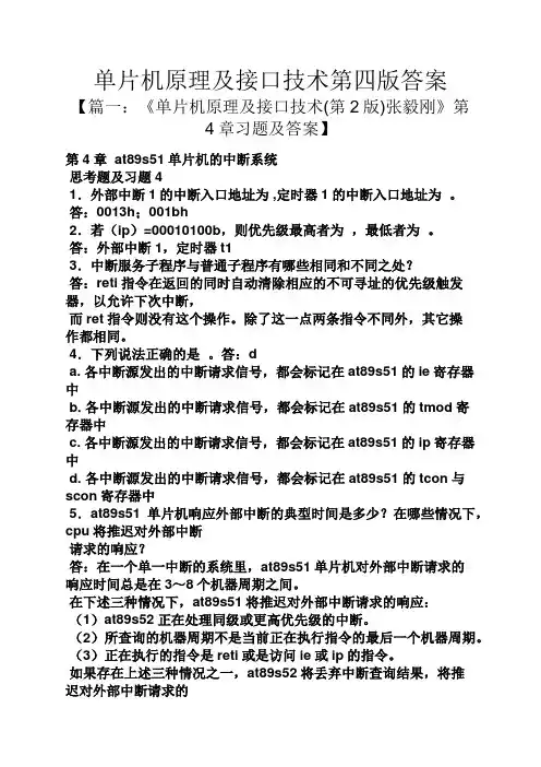
单片机原理及接口技术第四版答案【篇一:《单片机原理及接口技术(第2版)张毅刚》第4章习题及答案】第4章 at89s51单片机的中断系统思考题及习题41.外部中断1的中断入口地址为 ,定时器1的中断入口地址为。
答:0013h;001bh2.若(ip)=00010100b,则优先级最高者为,最低者为。
答:外部中断1,定时器t13.中断服务子程序与普通子程序有哪些相同和不同之处?答:reti指令在返回的同时自动清除相应的不可寻址的优先级触发器,以允许下次中断,而ret指令则没有这个操作。
除了这一点两条指令不同外,其它操作都相同。
4.下列说法正确的是。
答:da. 各中断源发出的中断请求信号,都会标记在at89s51的ie寄存器中b. 各中断源发出的中断请求信号,都会标记在at89s51的tmod寄存器中c. 各中断源发出的中断请求信号,都会标记在at89s51的ip寄存器中d. 各中断源发出的中断请求信号,都会标记在at89s51的tcon与scon寄存器中5.at89s51单片机响应外部中断的典型时间是多少?在哪些情况下,cpu将推迟对外部中断请求的响应?答:在一个单一中断的系统里,at89s51单片机对外部中断请求的响应时间总是在3~8个机器周期之间。
在下述三种情况下,at89s51将推迟对外部中断请求的响应:(1)at89s52正在处理同级或更高优先级的中断。
(2)所查询的机器周期不是当前正在执行指令的最后一个机器周期。
(3)正在执行的指令是reti或是访问ie或ip的指令。
如果存在上述三种情况之一,at89s52将丢弃中断查询结果,将推迟对外部中断请求的响应。
6.中断查询确认后,在下列各种at89s51单片机运行情况下,能立即进行响应的是。
a. 当前正在进行高优先级中断处理b. 当前正在执行reti指令c. 当前指令是div指令,且正处于取指令的机器周期d. 当前指令是mov a,r3答:d7. at89s51单片机响应中断后,产生长调用指令lcall,执行该指令的过程包括:首先把的内容压入堆栈,以进行断点保护,然后把长调用指令的16位地址送,使程序执行转向中的中断地址区。


CHAPTER 6© 2008 Pearson Education, Inc.6-1.*6-2.6-3.6-4.*6-5.a) F = (A + B) C Db) G = (A + B) (C + D)a) 3-input NAND gate 6 inputs 16 inputs 16 inputsThe longest path is from input C or D.0.073 ns + 0.073 ns + 0.048 ns + 0.073 ns = 0.267 nsa)b)c)4.03.02.01.06.05.08.07.09.0 ns6-6.6-7. 6-8.+If the rejection time for inertial delays is greater than the propagation delay, then an output change can occur before it can be predicted whether or not it is to occur due to the rejection time.For example, with a delay of 2 ns and a rejection time of 3 ns, for a 2.5 ns pulse, the initialedge will have already appeared at the output before the 3 ns has elapsed at which whether to reject or not is to be determined.a) The propagation delay is t pd = max(t PHL = 0.05, t PLH = 0.10) = 0.10 ns.Assuming that the gate is an inverter, for a positive output pulse, the following actually occurs:If the input pulse is narrower than 0.05 ns, no output pulse occurs so the rejection time is 0.05 ns. The resulting model predicts the following results, which differ from the actual delay behavior, but models the rejection behavior: :0.10 ns0.05 ns0.10 ns0.10 ns6-9. 6-10.*b) For a negative output pulse, the following actually occurs:The model predicts the following results, which differs from the actual delay behavior andthe actual rejection behavior:Overall, the model is inaccurate for both cases a and b, and provides a faulty rejectionmodel for case b. Using an average of t PHL and t PLH for t pd would improve the delayaccuracy of the model for circuit applications, but the rejection model still fails.0.10 ns0.05 ns0.15 ns0.10 ns0.10 nsa)There is a setup time violation at 28 ns. There is an inputb)There is a setup time violation just before 24 ns, There is an inputc)There is a setup time violation at 28ns.d)There is a hold time violation at 16ns and a setup time violation at 24ns.combination violation around 24 ns.combination violation around 24 ns.a) The longest direct path delay is from input X through the two XOR gates to the output Y.t delay = t pdXOR + t pdXOR = 0.20 + 0.20 = 0.40 nsb) The longest path from an external input to a positive clock edge is from input X through the XOR gate and the inverter to the B Flip-flop.t delay = t pdXOR + t pd INV + t sFF = 0.20 + 0.05 + 0.1 = 0.35 nsc) The longest path delay from the positive clock edge is from Flip-flop A through the two XOR gates to the output Y.t delay = t pdFF + 2 t pdXOR = 0.40 + 2(0.20) = 0.80 nsd) The longest path delay from positive clock edge to positive clock edge is from clock on Flip-flop A through t delay-clock edge to clock edge = t pdFF + t pdXOR + t pdINV + t sFF = 0.40 + 0.20 + 0.05 + 0.10 = 0.75 nse) The maximum frequency is 1/t delay- clock edge to clock edge. For this circuit, t delay-clock edge to clock edgeis 0.75 ns, so the maximum frequency is 1/0.75 ns = 1.33 GHz.the XOR gate and inverter to clock on Flip-flop B.into its environment. Calculation of this frequency cannot be performed in this case since data for paths through the environment is not provided.Comment: The clock frequency may need to be lower due to other delay paths that pass outside of the circuit6-11.6-12.a) The longest direct path delay is from input X through the four XOR gates to the output Y.t delay = 4 t pdXOR = 4(0.20) = 0.80 nsb) The longest path from an external input to a positive clock edge is from input X through three XOR gates and the inverter to the clock of the second B Flip-flop.t delay = 3 t pdXOR + t pd INV + t sFF = 3(0.20) + 0.5 + 0.1 = 0.75 nsc) The longest path delay from the positive clock edge is from the first Flip-flop A through the four XOR gates to the output Y.t delay = t pdFF + 4 t pdXORR = 0.40 + 4(0.20) = 1.2 nsd) The longest path delay from positive clock edge to positive clock edge is from the first Flip-flop A through three XOR gates and one inverter to the clock of the second Flip-flop B.t delay-clock edge to clock edge = t pdFF + 3 t pdXOR + t pdINV + t sFF = 0.40+ 3(0.20) + 0.5 + 0.1 = 1.15 nse) The maximum frequency is 1/t delay-clock edge to clock edge. For this circuit, the delay is 1.15 nsso the maximum frequency is 1/1.15 ns = 870 MHz.Comment: The clock frequency may need to be lower due to other delay paths that pass outside of the circuit into its environment. Calculation of this frequency cannot be performed in this case since data for paths through the environment is not provided.AA6-13.*(Errata: Change "32 X 8" to "64 X 8" ROM)6-14. 6-15.6-16.IN OUT IN OUT IN OUT IN OUT 0000000000 00000100000001 01101000000011 00101100000100 1000 0000010000 00010100010001 01111000010011 00111100010100 1001 0000100000 00100100100001 10001000100011 01001100100101 0000 0000110000 00110100110001 10011000110011 01011100110101 0001 0001000000 01000101000010 00001001000011 01101101000101 0010 0001010000 01010101010010 00011001010011 01111101010101 0011 0001100000 01100101100010 00101001100011 10001101100101 0100 0001110000 01110101110010 00111001110011 10011101110101 0101 0010000000 10000110000010 01001010000100 00001110000101 0110 0010010000 10010110010010 01011010010100 00011110010101 0111 0010100001 00000110100010 01101010100100 00101110100101 1000 0010110001 00010110110010 01111010110100 00111110110101 1001 0011000001 00100111000010 10001011000100 01001111000110 0000 0011010001 00110111010010 10011011010100 01011111010110 0001 0011100001 01000111100011 00001011100100 01101111100110 0010 0011110001 01010111110011 00011011110100 01111111110110 0011a)16 + 16 + 1 = 33 address bits and 16 + 1 = 17 output bits, 8G × 17b)8 + 8 + 1 + 1 = 18 address bits and 8 + 1 = 9 output bitsc) 4 × 4 = 16 address bits and 14 output bits are needed, 64K × 14XYZXYZXYZXYZA B C D1111111111111111B = XY + XY + YZC = YZ C = YZ + Z A = XY + XY + YZBy using A instead of A and YZ instead of Y in D, YZ can be shared by all four functions. Further, since A is the complement of B, terms XY and XY can be shared between A and B. Thus, only four product terms YZ, XY, XY, and Z are required.An inversion must be programmed for A.6-17.6-18.6-19.*XY ZXYZ X YZ XY Z XYZ111111111X YZ 11AB CDEF11A = XYB = X + YZC = XY + X Y + ZD = YZE = 0F = ZImplementation of A, D, and E requires only two terms, XY and YZ. Straightforward implementation of B, C, and F requires four terms, XY , XYZ, XYZ, and Z. By implementing B, C, and F, only three additional termsX, X Y , and Z are required. So we form the solution using five product terms: XY , YZ, X Y, X, and Z. The solution is described by the equations given with the six K-maps.ABC D A BC D A BC D A BC D W X Y Z The values given in the four K-maps come from Table 3-1 on page 99.100110001100001111110000110011001111100d d d d dd d d d d dd d d d ddd d d d d dd W = A B + BC DX = BC D + BC + BD Y = CD + C D Z = D In this case, shared terms are limited. One such term B C D is generated in W.Assume 3-input OR gates.ABC DABC D ABCD ABC D W 100110001100001111110000110011001111100d d d d dd d d d ddd d d d ddd d d d d dd W = A + BC + BDX = BC D + BC + BD Y= CD + C D Z = D Each of the equations above is implemented using one 3-input OR gate. Four gates are used.6-20.6-21.X Y ZXYZX YZX Y Z11111111A B CD1A = XZ + YZ + X YZ B = XY + YZ + X YC = A + XYD = XY + Z1111111111Figure 6-23 uses 3-input OR gates.A, B, and D each require three or fewer product terms so can be implemented with 3-input OR gates.C requires four terms so cannot be implemented with a 3-input OR gate. But because the first PAL device outputcan used as an input to implement other functions it can be assigned to A and A can then be used to implement C using just two inputs of a 3-input OR gate.A ABCDABCD F111111111111111111GFigure 6-23 uses 3-input OR gates.Straightforward implementation of F requires five prime implicants and of G requires four prime implicants, but only 3 inputs are available on the PAL OR gates. So sum-of-products that can be factored from F and G or both and implemented by the other PAL cells are needed. A single sum of products that will work is H = ABC + BCD + BCD. The terms of H are shown with dotted lines on the K-maps. Using H:F = H + CD + ABG =H + AB There are other possible functions for H and corresponding results for F and H.。

(一)课程教学目的和要求随着科学技术的不断进步,计算机在社会各个领域中的应用也不断得以发展,本课程是信息类基础课程之一,是一门学生学习掌握计算机硬件知识和汇编语言程序设计的入门课程。
通过本课程的学习使学生从理论和实践两方面掌握单片机的基本结构、工作原理、汇编语言程序设计方法、接口电路及单片机应用系统的设计方法,以求达到初步的单片机软硬件设计开发能力。
并为以后从事电子控制类的设计奠定理论基础和实践能力。
《单片机原理及应用》是信息类专业的一门重要专业基础必修课,是一门理论与实际紧密结合并对学生进行工程训练的课程。
通过本课程的教学,学生应掌握51系列单片机CPU、定时/计数器、存储器、串行通信、中断系统、I/O口的硬件结构,能用汇编语言进行程序设计,具备应用单片机知识分析解决工程实际问题,设计较复杂的单片机应用系统能力。
(二)课程教学重点和难点1、重点:硬件结构;指令系统;系统扩展和应用;外围接口技术。
2、难点:指令系统;外围接口技术。
(三)教学方法理论与实验相结合(四)课时安排总课时:64课时,其中:理论课时48,实验课时16。
(五)考核方式本课程的考核采取平时的形成性考核和课程结束时的笔试闭卷考试相结合的考核办法。
平时的考核主要有三个方面:课堂、课外、实验。
课堂考核依据出勤率、听课态度、课堂讨论表现等;课外考核主要依据作业、平时测试、课外的创新和发明等;实验考核依据实验完成的质量和数量等情况来评定。
(六)参考教材刘湘涛.江世明编著《单片机原理与应用》.电子工业出版社. 2006.第一章单片机基础知识教研室:计算机教研室教师姓名:申寿云教学过程1、问题牵引、导入新课(1)单片机是什么?它的主要特点和应用的领域。
(2)计算机中数据有哪些表示?二进制、八进制、十进制、十六进制;原码、反码、补码;ASCII码、BCD码。
2、课程内容本章的主要知识点有:知识点1:单片机的概念。
知识点2:单片机主流机型。
知识点3:80C51系列简介。