TDA7850四声道镀金功放模块产品规格书
- 格式:pdf
- 大小:1.44 MB
- 文档页数:13
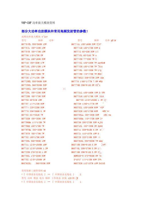
VHF-UHF功率放大模块资料部分大功率功放模块和常用高频发射管的参数!高频功率放大模块 t"Io*型号频率功率型号频率功率 gE\M M57704EL 335-360M 13W M67741L 135-160M 30W Y]O7M57704L 400-420M 13W M67741H 150-175M 30W kM57704H 450-470M 13W M67742 68-88M 30W 14)M57706 145-175M 8W M67743L 68-81M 7W oM57710A 156-160M 30W M67743H 77-88M 7W XM57716 430-450M 17W M67748L 135-150M 7W AqvKh@M57719L 135-145M 14W M67748H 150-175M 7W ?31xM57719 145-175M 14W M67749L 400-430M 7W L-gM57721L 350-400M 7W M67749H 440-470M 7W BKS!M57726 144-148M 43W M67760LC 806-870M 20W iQaM57729EL 335-360M 30W M67775 1465-1477M 7.5W wPpM57729SL 360-380M 30W M67776H 896-941M 5W CS~oM57729UL 400-420M 30W 4(M57729L 400-420M 30W M67781L 135-160M 40W D/4PNM57729H 450-470M 30W M67781H 150-175M 40W {di6M57735 50-54M 19W M67783 1240-1300M 1.4W ZJM57737 144-148M 30W M67789 1465-1477M 3W "M57774 220-225M 30W M68702L 135-160M 60W 'vUPM57775 806-866M 0.4W M68702H 150-175M 60W #RC'#/M57782 824-851M 7W M68703LA 400-430M 50W rEG =aM57788M 430-450M 40W M68703HA 440-470M 50W I*M57796MA 144-148M 7W M68706 250-270M 30W w_NdM57796H 150-175M 7W M68710L 400-430M 2W 5p#dM57797MA 430-450M 7W M68711 889-915M 3.8W :e`/`M57797H 450-470M 7W M68721 118-137M 10W &M67702 150-175M 60W M68729 220-245M 30W )4M67709L 350-390M 13W M68732SL 330-380M 7W aQq'M67711 1240-1300M 16W M68743H 896-941M 3.8W ]vP7M67715 1240-1300M 1.2W M68745L 806-870M 3.8W z\\M67723H 276-284M 1.5W M68745H 896-941M 3.8W I[_M67730L 175-200M 30W MHW803-3 870-905M 3W 75M67732 1240-1300M 1W S-AV17 144-148M 60W IV%M68762SL 360-380M 30W M68732H 118-137M 10W Do2xD常用发射三级管资料oX©『中国业余无线电』 -- 『中国业余无线电』X型号功率增益电压频率工作状态封装 123脚:[E©『中国业余无线电』 -- 『中国业余无线电』l2N3375 10W 5dB 28V 400MHz FM/AM/SSB TO-60]P2N3553 2,5W 10dB 28V 175MHz FM/AM TO-39 C B E2S\PD2N3632 20W 7dB 28V 175MHz FM TO-60g2N3866 5W 10dB 28V 400MHz WINTransceiver TO-39 C B ES2N3924 4W 6dB 13,6V 175MHz WINTransceiver TO-39?|.B2N4427 2W 10dB 12V 175MHz WINTransceiver TO-39l8N42N5108 1W 5dB 24V 1200MHz WINTransceiver TO-39 ]$Q2N5109 3,5W 11dB 15V 200MHz WINTransceiver TO-39({;8[#2N5421 3W 9dB 13,5V 175MHz WINTransceiver TO-39p7iTn2N5913 2W 7dB 12,5V 175MHz WINTransceiver TO-39h~}ETQ2N5943 1W 8dB 15V 400MHz FM TO-39z.2SC730 0,8W 10dB 13,5V 175MHz FM TO-39 C B E|2SC1096 10W 60MHz FM TO-2205Aa^2SC1173 10W 100MHz FM/AM/SSB TO-220-SF?:S2SC1306 16W 30MHz FM/AM/SSB TO-220 B C EP6Di!Y2SC1307 16W 12dB 12V 30MHz FM/AM/SSB TO-220 B C E~|97WO2SC1590 5W 10dB 12,5V 136-174MHz FM TO-220 B E C L(2SC1591 14W 7,5dB 12,5V 136-174MHz FM TO-220 B E C%2SC1678 5W 30MHz WINTransceiver TO-220 B C EZuG_N32SC1728 8W 80MHz WINTransceiver TO-202 E B Ca2SC1729 14W 10dB 13,5V 175MHz FM T-31ED~FW2SC1909 10W 14,5dB 13,5V 50MHz FM/AM/SSB TO-220 B C E(S#K,2SC1944 13W 11,1dB 12V 30MHz WINTransceiver TO-220 B C E>s?1Q2SC1945 16W 14,5dB 12V 30MHz FM/AM/SSB TO-220 B E C"&G02SC1946 25W 6,7dB 13,5V 175MHz FM T-31E{![5RK2SC1946A 30W 10dB 13,5V 175MHz FM T-31El2SC1947 3W 10dB 13,5V 175MHz FM TO-39 C B EO2SC1957 1,8W 17dB 12V 30MHz WINTransceiver TO-126 E C Bi@T2SC1966 3W 7,8dB 13,5V 470MHz FM T-31E_X52SC1967 7W 6,7dB 13,5V 470MHz FM T-31EKf2SC1968 14W 3,7dB 13,5V 470MHz FM T-31E>AS%e2SC1968A 14W 5,4dB 13,5V 470MHz FM T-31E]Nv)2SC1969 18W 12dB 12V 30MHz FM/AM/SSB TO-220 B C EZGtG]2SC1970 1,5W 10dB 13,5V 175MHz WINTransceiver TO-220 B E C~DmS7# 2SC1971 7W 10dB 13,5V 175MHz WINTransceiver TO-220 B E CjVWs2SC1972 14W 10dB 13,5V 175MHz WINTransceiver TO-220 B E C]e^0i2SC1973 1W 50MHz WINTransceiver TO-92L B C EfcPr2SC1974 13W 10dB 13,5V 30MHz WINTransceiver TO-220 B C E'S2SC1975 4W 10dB 13,5V 30MHz WINTransceiver TO-220 B C El'.2SC2028 1,8W 30MHz WINTransceiver TO-126 E C B>52SC2029 6W 30MHz WINTransceiver TO-220 B C E&Q2SC2036A 1,4W WINTransceiver TO-202 B C E_)bN{Q2SC2050 10W 12dB 13,5V 30MHz FM/AM/SSB TO-220 B C En,C_2SC2053 0,2W 15,7dB 12V 175MHz FM/AM TO-92L B C EGjVm02SC2055 0,25W 15,3dB 12V 175MHz FM/AM TO-92L B C Et2SC2056 1,5W 9dB 12V 175MHz FM TO-39 C B Ep\=_2SC2075 4W 13,5V 27MHz WINTransceiver TO-220 B C Eyc42SC2078 4W 13dB 12V 100MHz FM/AM TO-220 B C ECgb}2SC2086 0,45W 13dB 12V 175MHz FM/AM TO-92L B C E#g{2SC2092 4W 13dB 12V 100MHz FM/AM/SSB TO-220 B C EM2SC2094 15W 8,8dB 13,5V 175MHz FM/AM/SSB T-31EtS;2SC2166 6W 13,8dB 12V 30MHz FM/AM/SSB TO-220 B C Ee7/~2SC2207 16W WINTransceiver TO-220 B C Emt2SC2237 6W 13,8dB 13,5V 175MHz FM T-31E?)B32SC2312 18,5W 27MHz FM/AM/SSB TO-220 B C Eq+J2SC2314 1,8W 17dB 12V 180MHz FM/AM TO-126 E C BO2SC2509 13W 14dB 30MHz WINTransceiver TO-220 B C E$Y!2SC2527 60W WINTransceiver TO-220V2SC2538 0,6W 10dB 12V 175MHz FM/AM TO-92L B C Einy2SC2539 14W 14,5dB 13,5V 175MHz FM T-31Efhm02SC2660 30W 30MHz WINTransceiver TO-220DF2SC2695 23W 1,9dB 13,5V 520MHz FM T-31EX4@SK2SC3001 6W 13dB 7,2V 175MHz FM T-31E|2SC3017 1W 11dB 13,5V 175MHz FM TO-39 C B EA*2SC3018 3W 13dB 7,2V 175MHz FM T-31E=.2SC3020 3W 10dB 12,5V 520MHz FM T-31E:/a`"2SC3021 7W 7,7dB 12,5V 520MHz FM T-31E3A= x&2SC3022 18W 4,8dB 12,5V 520MHz FM T-31EM)5L|(2SC3103 2,8W 6,7dB 7,2V 520MHz FM T-31EGOIF/22SC3104 6W 4,8dB 7,2V 520MHz FM T-31ET4os2SC3133 13W 14dB 12V 1,5-30MHz FM/AM/SSB TO-220 B E CW2SC3297 15W 100MHz WINTransceiver TO-220Qu2SC3299 20W WINTransceiver TO-220#2SC3668 1W 100MHz WINTransceiver g$F<&.2SC3807 15W 260MHz WINTransceiver TO-126s2SC4137 4W 400MHz WINTransceiver TO-126$cv_B<2SC4693 FM/AM TO-92L B C EQ]4KTC1006 1W 100MHz FM/AM TO-92L E C BCKTC1969 16W 12dB 12V 100MHz FM/AM TO-220 B C Et,=XcuKTC2078 4W 11dB 12V 100MHz FM/AM TO-220 B C E 6&PYNMRF161 5W 13,5dB 12,5V 225-500MHz FM/AM TO-220 B E C~CcMyMRF162 15W 13,5dB 12,5V 225-500MHz FM/AM TO-220 B E C)MRF163 25W 12dB 12,5V 225-500MHz FM/AM TO-220 B E C$&X>5MRF237 4W 12dB 18V 175MHz WINTransceiver TO-390sj4vQMRF260 5W 10dB 12,5V 136-174MHz FM TO-220 B E C^IMRF261 10W 5,2dB 12,5V 136-174MHz FM TO-220 B E C[/MRF262 14W 7,5dB 12,5V 136-174MHz FM TO-220 B E C`N>U`MRF264 30W 5,2dB 12,5V 136-174MHz WINTransceiver TO-220 B E CK&fhMRF340 8W 13dB 28V 70MHz WINTransceiver TO-220 B E CdMRF342 24W 11dB 28V 70MHz WINTransceiver TO-220 B E CSg95MRF344 60W 6dB 28V 70MHz WINTransceiver TO-220MuyUMRF454 80W 12dB 12,5V 1,5-30MHz FM/AM/SSB BgEMRF455 60W 13dB 12,5V 1,5-30MHz FM/AM/SSB i)2MRF475 12W 10dB 13,5V 1,5-30MHz FM/AM/SSB TO-220 B C EY?Z- | MRF476 3W 15dB 13,5V 1,5-30MHz FM/AM/SSB TO-220 B C E|%lMRF477 40W 15dB 13,5V 1,5-30MHz FM/AM/SSB TO-220 B E C[JM;0 MRF479 15W 10dB 13,5V 1,5-30MHz FM/AM/SSB TO-220a/e<.iMRF485 15W 10dB 28V 1,5-30MHz WINTransceiver TO-220SMRF486 40W 15dB 28V 1,5-30MHz WINTransceiver TO-220i{JgODMRF496 40W 15dB 13,5V 1,5-30MHz WINTransceiver TO-220Y;g6MRF497 60W 10dB 13,5V 27-50MHz WINTransceiver TO-220 B E CLm|kg MRF517 0,75W 10dB 20V 1000MHz WINTransceiver TO-39y]zmzjMRF607 1,75W 11,5dB 16V 175MHz WINTransceiver TO-39w>zMRF660 7W 5,4dB 12,5V 400-512MHz WINTransceiver TO-220#gz[MS1226 30W 18dB 28V 30MHz FM/AM/SSB z2j$AMS1227 20W 15dB 12,5V 30MHz FM/AM/SSB Xp&$Q无线电台常用高频发射管参数型号电流功率频率型号电流功率频率C1945 6A 20W 30MHz C2538 0.4A 0.7W 175MHzC1969 6A 20W 30MHz C2539 4A 35W 175MHzC2078 3A 10W 30MHz C2628 4A 40W 175MHzC2904 22A 200W 37MHz C2630 14A 100W 175MHzC1162 2.5A10W 37MHz C2694 20A 140W 175MHzC1946 7A 50W 175MHz C2905 15A 120W 520MHzC1947 1A 10W 175MHz C3101 1A 10W 520MHzC1970 0.6A5W 175MHz C3102 18A 170W 520MHzC1971 2A 13W 175MHz C3022 7A 50W 520MHzC1972 4A 25W 175MHz C1947 1A 10W 175MHzC2053 0.3A0.6W 175MHz C1959 0.5A 0.5W 300MHzC2131 0.6A4W 520MHz C2068 0.5A 1.5W 95MHzC2407 0.2A0.6W 500MHz C2229 0.5A 0.8W 120MHzC2482 0.7A0.9W 50MHz型号功率增益电压频率工作状态封装 123脚国外三极管2N3375 10W 5dB 28V 400MHz FM/AM/SSB TO-602N3553 2.5W 10dB 28V 175MHz FM/AM TO-39 C B E2N3632 20W 7dB 28V 175MHz FM TO-602N3866 5W 10dB 28V 400MHz WINTransceiver TO-39 C B E2N3924 4W 6dB 13.6V 175MHz WINTransceiver TO-392N4427 2W 10dB 12V 175MHz WINTransceiver TO-392N5108 1W 5dB 24V 1200MHz WINTransceiver TO-392N5109 3.5W 11dB 15V 200MHz WINTransceiver TO-392N5421 3W 9dB 13.5V 175MHz WINTransceiver TO-392N5913 2W 7dB 12.5V 175MHz WINTransceiver TO-392N5943 1W 8dB 15V 400MHz FM TO-392SC730 0.8W 10dB 13.5V 175MHz FM TO-39 C B E2SC1096 10W 60MHz FM TO-2202SC1173 10W 100MHz FM/AM/SSB TO-2202SC1306 16W 30MHz FM/AM/SSB TO-220 B C E2SC1307 16W 12dB 12V 30MHz FM/AM/SSB TO-220 B C E2SC1590 5W 10dB 12.5V 136-174MHz FM TO-220 B E C2SC1591 14W 7.5dB 12.5V 136-174MHz FM TO-220 B E C2SC1674 0.5W 18dB 30V 600MHz FM/AM E C B2SC1675 0.5W 50V 250MHz FM/AM2SC1678 5W 30MHz WINTransceiver TO-220 B C E2SC1728 8W 80MHz WINTransceiver TO-202 E B C2SC1729 14W 10dB 13.5V 175MHz FM T-31E2SC1906 0.1W 18dB 12V 1000MHz FM2SC1907 0.1W 30V 1100MHz FM2SC1909 10W 14.5dB 13.5V 50MHz FM/AM/SSB TO-220 B C E2SC1944 13W 11.1dB 12V 30MHz WINTransceiver TO-220 B C E2SC1945 16W 14.5dB 12V 30MHz FM/AM/SSB TO-220 B E C2SC1946 25W 6.7dB 13.5V 175MHz FM T-31E2SC1946A 30W 10dB 13.5V 175MHz FM T-31E2SC1947 3W 10dB 13.5V 175MHz FM TO-39 C B E2SC1957 1.8W 17dB 12V 30MHz WINTransceiver TO-126 E C B2SC1966 9W 7.8dB 13.5V 470MHz FM T-31E2SC1967 7W 6.7dB 13.5V 470MHz FM T-31E2SC1968 14W 3.7dB 13.5V 470MHz FM T-31E2SC1968A 14W 5.4dB 13.5V 470MHz FM T-31E2SC1969 18W 12dB 12V 30MHz FM/AM/SSB TO-220 B C E2SC1970 1.5W 9.2dB 13.5V 175MHz WINTransceiver TO-220 B C E 2SC1971 7W 10dB 13.5V 175MHz WINTransceiver TO-220 B E C2SC1972 14W 7.5dB 13.5V 175MHz WINTransceiver TO-220 B E C 2SC1973 1W 50MHz WINTransceiver TO-92L B C E2SC1974 13W 10dB 13.5V 30MHz WINTransceiver TO-220 B C E2SC1975 4W 10dB 13.5V 30MHz WINTransceiver TO-220 B C E2SC2028 1.8W 30MHz WINTransceiver TO-126 E C B2SC2029 6W 30MHz WINTransceiver TO-220 B C E2SC2036A 1.4W ***** WINTransceiver TO-202 B C E2SC2050 10W 12dB 13.5V 30MHz FM/AM/SSB TO-220 B C E2SC2053 0.2W 15.7dB 12V 175MHz FM/AM TO-92L B C E2SC2055 0.25W 15.3dB 12V 175MHz FM/AM TO-92L B C E2SC2056 1.5W 9dB 12V 175MHz FM TO-39 C B E2SC2075 4W 13.5V 27MHz WINTransceiver TO-220 B C E2SC2078 4W 13dB 12V 100MHz FM/AM TO-220 B C E2SC2086 0.45W 13dB 12V 175MHz FM/AM TO-92L B C E2SC2092 4W 13dB 12V 100MHz FM/AM/SSB TO-220 B C E2SC2094 15W 8.8dB 13.5V 175MHz FM/AM/SSB T-31E2SC2166 6W 13.8dB 12V 30MHz FM/AM/SSB TO-220 B C E2SC2207 16W 27MHz WINTransceiver TO-220 B C E2SC2237 6W 13.8dB 13.5V 175MHz FM T-31E2SC2312 18.5W 27MHz FM/AM/SSB TO-220 B C E2SC2314 1.8W 17dB 12V 180MHz FM/AM TO-126 E C B2SC2509 13W 14dB 30MHz WINTransceiver TO-220 B C E2SC2527 60W 80MHZ WINTransceiver TO-2202SC2538 0.6W 10dB 12V 175MHz FM/AM TO-92L B C E2SC2539 14W 14.5dB 13.5V 175MHz FM T-31E2SC2558 1.3W 12dB 960MHz2SC2630 60W 175MHz2SC2660 30W 30MHz WINTransceiver TO-2202SC2668 0.1W 18dB 40V 550MHz FM2SC2695 30W 5dB 13.5V 520MHz FM T-31E2SC2851 0.9W 9dB 175MHz FM2SC2905 50W 5dB 512MHz2SC2932 6W 8dB 960MHz2SC3001 6W 13dB 7.2V 175MHz FM T-31E2SC3017 1W 11dB 13.5V 175MHz FM TO-39 C B E2SC3018 3W 13dB 7.2V 175MHz FM T-31E2SC3019 0.6W 14dB 512MHz2SC3020 3W 10dB 12.5V 520MHz FM T-31E2SC3021 7W 7.7dB 12.5V 520MHz FM T-31E2SC3022 18W 4.8dB 12.5V 520MHz FM T-31E2SC3103 2.8W 6.7dB 7.2V 520MHz FM T-31E2SC3104 6W 4.8dB 7.2V 520MHz FM T-31E2SC3133 13W 14dB 12V 1.5-30MHz FM/AM/SSB TO-220 B E C 2SC3174 60W 7dB 175MHz2SC3297 15W 100MHz WINTransceiver TO-2202SC3299 20W 120MHz WINTransceiver TO-2202SC3355 0.6W 12V 6500MHz FM/TV B E C2SC3358 0.5W 12V 7000MHz UHF2SC3668 1W 50V 100MHz WINTransceiver2SC3700 30W 960MHz2SC3702 80W 960MHz2SC3807 15W 260MHz WINTransceiver TO-1262SC4137 4W 400MHz WINTransceiver TO-1262SC4167 8W 8dB 512MHz2SC4693 0.9W 12V 2500MHz FM/AM TO-92L B C E2SD467 0.5W 12V 280MHz FM/AM2SD468 0.9W 12V 190MHz FM/AMBFQ43 4W 12dB 13.5V 175MHzBFR96 0.3W 13.5dB 12V 5000MHz UHFBFR96S 0.5W 9dB 12V 5000MHz UHFBLT50 1.2W 512MHzBLT53 8W 7dB 512MHzBLT80 0.8W 6dB 960MHzBLT81 1.2W 7dB 960MHzBLU99 5W 10dB 512MHzBLV59 30W 11dB 900MHzBLV97 35W 11dB 900MHzBLV99 2W 11dB 900MHzBLV100 8W 11dB 900MHzBLV101 50W 11dB 900MHzBLV103 4W 11dB 900MHzBLV2045 35W 9dB 2000MHzBLW81 10W 7dB 512MHzBLX65 2W 9dB 512MHzBLY87C 8W 12dB 175MHzBLY88A 15W 9dB 175MHzKTC1006 1W 100MHz FM/AM TO-92L E C BKTC1969 16W 12dB 12V 100MHz FM/AM TO-220 B C EKTC2078 4W 11dB 12V 100MHz FM/AM TO-220 B C EMGF0905 40W 34dB 2000MHzMLF503 3W 11dB 7.5V 500MHzMLF507 7W 11dB 12V 500MHzMFF208 10W 11dB 2000MHzMRF134 5W 14dB 400MHzMRF136 15W 16dB 400MHzMRF161 5W 13.5dB 12.5V 225-500MHz FM/AM TO-220 B E CMRF162 15W 13.5dB 12.5V 225-500MHz FM/AM TO-220 B E CMRF163 25W 12dB 12.5V 225-500MHz FM/AM TO-220 B E CMRF182 30W 14dB 1000MHzMRF184 60W 11.5dB 1000MHzMRF237 4W 12dB 18V 175MHz WINTransceiver TO-39MRF260 5W 10dB 12.5V 136-174MHz FM TO-220 B E CMRF261 10W 5.2dB 12.5V 136-174MHz FM TO-220 B E CMRF262 14W 7.5dB 12.5V 136-174MHz FM TO-220 B E CMRF264 30W 5.2dB 12.5V 136-174MHz WINTransceiver TO-220 B E C MRF314 30W 10dB 175MHzMRF340 8W 13dB 28V 70MHz WINTransceiver TO-220 B E CMRF342 24W 11dB 28V 70MHz WINTransceiver TO-220 B E CMRF344 60W 6dB 28V 70MHz WINTransceiver TO-220MRF454 80W 12dB 12.5V 1.5-30MHz FM/AM/SSBMRF455 60W 13dB 12.5V 1.5-30MHz FM/AM/SSBMRF475 12W 10dB 13.5V 1.5-30MHz FM/AM/SSB TO-220 B C E MRF476 3W 15dB 13.5V 1.5-30MHz FM/AM/SSB TO-220 B C EMRF477 40W 15dB 13.5V 1.5-30MHz FM/AM/SSB TO-220 B E C MRF479 15W 10dB 13.5V 1.5-30MHz FM/AM/SSB TO-220MRF485 15W 10dB 28V 1.5-30MHz WINTransceiver TO-220MRF486 40W 15dB 28V 1.5-30MHz WINTransceiver TO-220MRF496 40W 15dB 13.5V 1.5-30MHz WINTransceiver TO-220MRF497 60W 10dB 13.5V 27-50MHz WINTransceiver TO-220 B E C MRF517 0.75W 10dB 20V 1000MHz WINTransceiver TO-39MRF553 1.5W 9dB 175MHzMRF559 0.5W 900MHzMRF607 1.75W 11.5dB 16V 175MHz WINTransceiver TO-39MRF630 4W 10dB 13.5V 512MHz FM TO-39MRF650 50W 5dB 512MHzMRF652 5W 10dB 512MHzMRF859 6.5W 11dB 900MHzMRF660 7W 5.4dB 12.5V 400-512MHz WINTransceiver TO-220 MRF844 30W 960MHzMRF846 40W 960MHzMRF847 45W 960MHzMRF857 2W 11dB 900MHzMRF858 3.6W 11dB 900MHzMRF891 5W 9dB 900MHzMRF899 150W 11dB 900MHzMRF2062 1.2W 15dB 2000MHzMRF2628 15W 12dB 175MHzMRF8372 0.75W 8dB 960MHzMRF20060 60W 9dB 2000MHzMRF20082 15W 9dB 2000MHzMRF20146 0.6W 10dB 2000MHzMRF20147 4W 10dB 2000MHzMRF20170 30W 8.5dB 2000MHzMS1226 30W 18dB 28V 30MHz FM/AM/SSBMS1227 20W 15dB 12.5V 30MHz FM/AM/SSBSD1477 100W 175MHzTP3007 2W 9dB 900MHzTP3008 4W 11.5dB 900MHzTP3020 2.2W 9dB 900MHzTP3022 15W 9dB 900MHzTP3024 35W 7.5dB 900MHzTP5002 2W 13dB 510MHzTP5015 15W 11dB 510MHz国内三极管3DA21A 7.5W 10dB 15V 400MHz FM/AM3DA21B 7.5W 10dB 25V 400MHz FM/AM3DA22A 15W 10dB 15V 400MHz FM/AM3DA22B 15W 10dB 25V 400MHz FM/AM3DA23A 30W 15V 500MHz FM/AM3DA23B 30W 12V 500MHz FM/AM3DA23C 30W 20V 500MHz FM/AM3DA24A 2W 15V 1000MHz FM3DA24B 2W 15V 1000MHz FM3DA190 2W 35V 600MHz3DA191 5W 35V 600MHz3DA192 7.5W 35V 600MHz3DA193 15W 35V 600MHz3DA194 2W 35V 1GHz常用高频放大等配件参考报价表:C1907 1.1G 0.3W 0.70 BFR90 5G 0.2W 2.80 C2570 5G 0.3W 1.20 BFR91A 5G 0.25W 1.90 C3355 6.5G 0.6W 1.30 BFR96S 5G 0.35W 1.90 C3358 7G 0.25W 5.00 MRF571 8G 1W 9.00 BFQ34 3.5G 2.5W 108.00 MRF581 5G 2.5W 6.00 BFW16A 1.5G 1.5W 9.00 MRF587 5.5G 10W 150.00 LP1001 5G 0.25W 1.20型号电流功率频率报价(元/只)型号电流功率频率报价(元/只)C1945 6A 14W 27M 34.00 C2694 20A 70W 175M 180.00 C1946A 7A 30W 175M 75.00 C2695 10A 30W 520M 195.00 C1947 1A 3.5W 175M 34.00 C2782 20A 80W 175M 260.00 C1969 6A 16W 27M 15.00 C2879 25A 120W 28M 328.00 C1970 0.6A 1W 175M 9.00 C2904 22A 100W 30M 180.00 C1971 2A 6W 175M 16.00 C2905 15A 45W 520M 185.00C1972 4A 18W 175M 55.00 C3019 0.4A 0.5W 520M 18.00 C2053 0.3A 0.15W 175M 4.00 C3020 1A 3W 520M 80.00 C2078 3A 4W 27M 5.00 C3021 2A 7W 520M 120.00 C2131 0.6A 1.4W 520M 34.00 C3022 7A 18W 520M 128.00 C2166 4A 6W 27M 10.00 C3101 1A 3W 50M 43.00 C2237 2A 6W 175M 39.00 C3102 18A 60W 520M 298.00 C2407 0.15A 0.16W 500M 4.50 C3133 6A 13W 27M 34.00 C2510 20A 150W 28M 620.00 C3240 25A 110W 30M 210.00 C2538 0.4A 0.6W 175M 6.50 C3908 25A 110W 30M 278.00 C2539 4A 18W 175M 58.00 C4624 15A 45W 900M 258.00 C2628 4A 18W 175M 90.00 C4989 20A 65W 520M 310.00 C2629 8A 30W 175M 148.00 C5125 25A 80W 175M 258.00 C2630 14A 50W 175M 120.00 MRF247 20A 80W 175M 210.00高频功率放大模块型号频率功率报价(元/只)型号频率功率报价(元/只)M57704EL 335-360M 13W 238 M67741L 135-160M 30W 290 M57704L 400-420M 13W 210 M67741H 150-175M 30W 290 M57704H 450-470M 13W 210 M67742 68-88M 30W 500 M57706 145-175M 8W 210 M67743L 68-81M 7W 290 M57710A 156-160M 30W 170 M67743H 77-88M 7W 290 M57716 430-450M 17W 290 M67748L 135-150M 7W 136 M57719L 135-145M 14W 210 M67748H 150-175M 7W 136 M57719 145-175M 14W 210 M67749L 400-430M 7W 136 M57721L 350-400M 7W 210 M67749H 440-470M 7W 136 M57726 144-148M 43W 355 M67760LC 806-870M 20W 520 M57729EL 335-360M 30W 368 M67775 1465-1477M 7.5W 660 M57729SL 360-380M 30W 368 M67776H 896-941M 5W 648 M57729L 400-420M 30W 310 M67781L 135-160M 40W 540 M57729H 450-470M 30W 310 M67781H 150-175M 40W 540 M57735 50-54M 19W 380 M67783 1240-1300M 1.4W 406 M57737 144-148M 30W 310 M67789 1465-1477M 3W 720 M57774 220-225M 30W 248 M68702L 135-160M 60W 496 M57775 806-866M 0.4W 128 M68702H 150-175M 60W 496 M57782 824-851M 7W 358 M68703LA 400-430M 50W 520 M57788M 430-450M 40W 460 M68703HA 440-470M 50W 530 M57796MA 144-148M 7W 110 M68706 250-270M 30W 338 M57796H 150-175M 7W 110 M68710L 400-430M 2W 168M57797MA 430-450M 7W 110 M68711 889-915M 3.8W 318 M57797H 450-470M 7W 110 M68721 118-137M 10W 248 M67702 150-175M 60W 720 M68729 220-245M 30W 328 M67709L 350-390M 13W 540 M68732SL 330-380M 7W 180 M67711 1240-1300M 16W 430 M68743H 896-941M 3.8W 285 M67715 1240-1300M 1.2W 380 M68745L 806-870M 3.8W 96 M67723H 276-284M 1.5W 218 M68745H 896-941M 3.8W 396 M67730L 175-200M 30W 450 MHW803-3 870-905M 3W 168 M67732 1240-1300M 1W 345 S-AV17 144-148M 60W 350 M68762SL 360-380M 30W 426型号种类报价(元/只)型号种类报价(元/只)BA1404 调频发射 6.00 MC3359P 调频中频 5.0038KHz 频差20PPm3.50 MC3361P 调频中频4.00BB910 变容管 2.5 MC3361(贴片) 调频中频 4.50 TA7673 调制器8.00 MC3362D(贴片) 调频接收 15.00 UC3842 电源控制 3.50 MC3367DW 调频接收 18.00 UPC1241H 功放10.00 MC12022A 分频器30.00 NE564 伴音解调12.00 MC145106P 频率合成 19.00 NE575N 频率压扩19.50 MC145146P 频率合成 35.00 NE576N 频率压扩10.00 MC145151P2 频率合成 30.00 NE576D(贴片) 频率压扩11.00 MC145152P2 频率合成 30.00 NE592 视频放大 3.50 MC145026 编码 5.00 NE602 混频12.00 MC145027 解码 5.00 NE604 中频放大25.00 MC145028 解码 6.00NJM2902 低功耗四运放2.80 MC145030 编解码12.00UM3750 编译码8.00 MC145436P 编解码10.00 UM3753 编译码8.00 VD5026-4 解码 3.50 UM3758-108A 编译码9.50 VD5027-4 解码 3.50 UM3758-108AM(贴片)编译码9.80 VD5028-4 解码 4.50 M51304L 低噪放大19.80 CM8870P1 编码 6.00 MB504L 分频器21.00 CM8880P1 编解码32.00 MB1504PF(贴片) 频率合成30.00 MT8870CE 编码 6.50MB3713 功放38.00 TA8164P 调频调幅接收3.80MB3756 电源调控38.00 TDA7010T 调频接收 6.00转换LA4422 功放30.00 TDA7021T 调频接收 6.00MC1377P 彩色编码15.00 TDA7050T 立体声功放3.80MC2831P 调频发射 5.00 TDA7088T 调频接收 6.00 MC2833P 调频发射 4.00MC2833D(贴片) 调频发射 6.00MC3357P 调频中频 4.00。

TDA7850反馈电容1. 引言TDA7850是一种常用的音频功放芯片,广泛应用于车载音响系统、家庭影院系统等领域。
在TDA7850芯片的设计中,反馈电容起到了至关重要的作用。
本文将对TDA7850反馈电容的功能、选择和优化进行全面详细的介绍。
2. TDA7850芯片概述TDA7850是意法半导体公司(STMicroelectronics)生产的一款四声道BTL(桥接式)音频功放芯片。
它采用了多级反馈配置,能够提供高质量、高效率的音频功放输出。
在TDA7850芯片中,反馈电容是实现负反馈的关键元件之一。
3. 反馈电容的功能反馈电容在TDA7850的设计中起到了重要的功能和作用,主要包括以下几个方面:3.1. 频率响应控制反馈电容通过控制芯片的反馈回路,能够对音频功放的频率响应进行调节。
在TDA7850中,通过合适的选择和设计反馈电容,可以实现增益的平坦性、低频的放大和高频的衰减,从而达到更好的音频效果。
3.2. 噪声抑制反馈电容能够对输入信号的噪声进行抑制。
它通过将部分输出信号与输入信号进行比较,并通过反馈回路将误差信号减小,从而减少噪音的影响。
在TDA7850中,通过合适的反馈电容设计,可以有效降低功放输出的噪声水平。
3.3. 稳定性改善反馈电容对提高音频功放的稳定性也有重要的作用。
通过选择合适的反馈电容参数,可以提高芯片的稳定性,减少输出的失真和不稳定因素,从而获得更好的音频性能。
4. 反馈电容的选择在选择TDA7850反馈电容时,可以考虑以下几个因素:4.1. 容值选择反馈电容的容值决定了反馈电路的带宽和频率响应范围。
一般来说,容值较大的反馈电容可以提供更宽的带宽和更平坦的频率响应。
但是,在实际选择中需要考虑成本、空间和制造工艺等因素。
根据具体的应用需求,选择适当的容值是关键。
4.2. 电压选择反馈电容的电压要求应该大于功放芯片的工作电压,以确保其可靠性和稳定性。
同时,还需要考虑反馈电容耐压的安全裕度,以应对可能的电压冲击和峰值。

tda 7850反馈电容一、什么是TDA 7850反馈电容?TDA 7850反馈电容是一种电子元件,它被广泛应用于音频放大器电路中。
它的作用是在音频放大器中提供反馈回路,以稳定放大器的工作状态,并降低失真和噪声。
二、TDA 7850反馈电容的工作原理TDA 7850反馈电容的工作原理与普通的电容相似,它可以在两个导体之间存储电荷。
当信号通过音频放大器时,它会被输入到反馈回路中,然后被传送到TDA 7850反馈电容。
在这里,它会被存储为一个静电充电,并且在放大器输出端口产生一个反向信号。
这个反向信号将与输入信号进行比较,并根据需要进行调整。
这样就可以实现放大器的自动校正和稳定。
三、TDA 7850反馈电容的参数1. 容量:TDA 7850反馈电容通常具有1uF或2.2uF的容量。
2. 工作温度:-40℃至+105℃。
3. 额定电压:50V至100V。
4. 封装类型:TDA 7850反馈电容通常采用SMD封装。
四、TDA 7850反馈电容的应用TDA 7850反馈电容广泛应用于音频放大器中,以提高放大器的性能和稳定性。
它可以降低失真和噪声,并提高输出功率和频率响应。
此外,TDA 7850反馈电容还可以在其他电路中使用,例如DC-DC转换器、LED驱动器等。
五、如何正确选择TDA 7850反馈电容?1. 容量:根据具体的应用需求选择合适的容量。
2. 工作温度:根据实际工作环境选择适合的工作温度范围。
3. 额定电压:根据实际工作电压选择适合的额定电压。
4. 封装类型:根据具体的使用场景选择适合的封装类型。
六、如何正确安装TDA 7850反馈电容?1. 在安装前,请检查TDA 7850反馈电容是否损坏或变形。
2. 在安装时,请注意极性,并将正极连接到正极端口,负极连接到负极端口。
3. 在焊接时,请使用正确的焊接工具和技术,并遵循正确的焊接流程。
4. 在安装后,请检查焊接点是否牢固,是否存在短路或开路等问题。

TDA7375、TDA7377、TDA7379 HIFI 2.1声道功放模块产品规格书浙江剑飞电子目录前言 (3)一、芯片兼容 (4)二、板载材料标准 (4)2.1产品PCB标准 (4)2.2主芯片(TDA7375/TDA7377/TDA7379) (5)2.3前级芯片(4558/5532/AD827) (5)2.4板载电容 (6)2.4.1黑金刚 (6)2.4.2红宝石( Rubycon) (6)2.4.3日本埃尔纳公司(ELNA) (7)2.4.4威马(WIMA) (7)2.4.5爱普科斯(EPCOS) (8)2.4.6 台湾立隆 (8)2.4.7电容板载 (8)2.5其它配件材料 (9)2.5.1电位器 (9)2.5.2整流桥 (10)2.5.3莲花接线座 (10)2.5.4接线端子 (10)2.5.5稳压模块 (10)三、电路设计 (10)3.1技术指标 (11)3.2布局和接线 (12)3.3音箱选配配置参考 (13)四、元器件清单 (14)五、HIFI 2.1成品模块图片 (15)前言TDA7375/TDA7377/TDA7379是ST公司(意法半导体公司全球第五大半导体公司服务所有电子细分市场的领先集成器件制造商)生产的双声道汽车专用IC这款芯片采用的是BTL的输出形式,外围原件极少但是音质极佳,安装也非常的方便,封装为15脚双列直插式。
电源供电为直流12V-15V,本款产品为2.1声道功放模块,采用最通用的电路模式设计理念也非常的符合IC的整体效果。
套件的用料也极其讲究威马专用的音频电容,小容量电容全部采用西门子薄膜电容系列,电解电容采用(黑金刚、红宝石、ELNA)三个牌子的原装品牌电容,台湾立隆10000uF滤波电容,为了方便连接,本板的输入采用莲花座输入,输出全部采用了0.5mm的接线端子,方便外接连线。
套件PCB使用优质双面玻纤板,优质蓝色阻焊层,布局合理,美观大方。
外围元件少,无噪音,低音低沉有力,中高音饱满清晰,音质纯净。

PRODUCT SUMMARYSKY77807 Quad-Band Power Amplifier Module for FDD/TDD LTE (Tx Bands 7, 38, 40, 41)Applications•Multi-band 4G handsets •Long Term Evolution (LTE)-Up to 20 MHz bandwidth/ 100resource blocks Features•Envelope Tracking(ET)FDD band•Average Power Tracking (APT) for TDD/FDD bands•50 ohm input/output impedance with internal DC-blocking •Fully programmable Mobile Industry Processor Interface digital control •Continuous bias control for3G/4G PA High Power Mode via MIPI/RFFE interface•Low Supply voltage•Low voltage support (0.6 V) for APT/SMPS applications •Low Leakage current in power-down mode •Temperature Sensor •Integrated TDD TX-Rx switch for single SAW architecture •Low voltage support forAPT/SMPS applications •Small, low profile package-4.0x 3.0x 1.0 (Max.) mm-24-pad configurationDescriptionThe SKY77807Quad-Band Power Amplifier Module (PAM) is a fully matched, 24-pad surface mount module developed for 4G LTE applications. The PAM consists of PA blocks, input and output matching, and a MIPI standard logic control block for multiple power control levels, output input switch control in a single 4.0mm x 3.0mm x 1.0 (Max.)mm package.The SKY77807uses an enhanced architecture to cover multiple bands and meet the spectral linearity requirements of LTE QPSK and 16QAM modulations with up to 20 MHz bandwidth and up to 100 resource block allocations. Output power is controlled by varying the input power and VCC is adjusted using an ET modulator or DCDC converter to maximize efficiency for each power level. Extremely low leakage current maximizes handset standby time.Skyworks Solutions, Inc. • Phone [781] 376-3000 • Fax [781] 376-3100•*********************•203049C• Skyworks Proprietary Information. • Products and product information are subject to change without notice. • January 13, 20141Ordering InformationProduct Name Order Number Evaluation Board Part NumberSKY77807SKY77807© 2013,Skyworks Solutions, Inc. All Rights Reserved.Information in this document is provided in connection with Skyworks Solutions, Inc. (“Skyworks”) products or services. These materials, including the information contained herein, are provided by Skyworks as a service to its customers and may be used for informational purposes only by the customer. Skyworks assumes no responsibility for errors or omissions in these materials or the information contained herein. Skyworks may change its documentation, products, services, specifications or product descriptions at any time, without notice. Skyworks makes no commitment to update the materials or information and shall have no responsibility whatsoever for conflicts, incompatibilities, or other difficulties arising from any future changes.No license, whether express, implied, by estoppel or otherwise, is granted to any intellectual property rights by this document. Skyworks assumes no liability for any materials, products or information provided hereunder, including the sale, distribution, reproduction or use of Skyworks products, information or materials, except as may be provided in Skyworks Terms and Conditions of Sale.THE MATERIALS, PRODUCTS AND INFORMATION ARE PROVIDED “AS IS” WITHOUT WARRANTY OF ANY KIND, WHETHER EXPRESS, IMPLIED, STATUTORY, OR OTHERWISE, INCLUDING FITNESS FOR A PARTICULAR PURPOSE OR USE, MERCHANTABILITY, PERFORMANCE, QUALITY OR NON-INFRINGEMENT OF ANY INTELLECTUAL PROPERTY RIGHT; ALL SUCH WARRANTIES ARE HEREBY EXPRESSLY DISCLAIMED. SKYWORKS DOES NOT WARRANT THE ACCURACY OR COMPLETENESS OF THE INFORMATION, TEXT, GRAPHICS OR OTHER ITEMS CONTAINED WITHIN THESE MATERIALS. SKYWORKS SHALL NOT BE LIABLE FOR ANY DAMAGES, INCLUDING BUT NOT LIMITED TO ANY SPECIAL, INDIRECT, INCIDENTAL, STATUTORY, OR CONSEQUENTIAL DAMAGES, INCLUDING WITHOUT LIMITATION, LOST REVENUES OR LOST PROFITS THAT MAY RESULT FROM THE USE OF THE MATERIALS OR INFORMATION, WHETHER OR NOT THE RECIPIENT OF MATERIALS HAS BEEN ADVISED OF THE POSSIBILITY OF SUCH DAMAGE.Skyworks products are not intended for use in medical, lifesaving or life-sustaining applications, or other equipment in which the failure of the Skyworks products could lead to personal injury, death, physical or environmental damage. Skyworks customers using or selling Skyworks products for use in such applications do so at their own risk and agree to fully indemnify Skyworks for any damages resulting from such improper use or sale.Customers are responsible for their products and applications using Skyworks products, which may deviate from published specifications as a result of design defects,errors, or operation of products outside of published parameters or design specifications. Customers should include design and operating safeguards to minimize these and other risks. Skyworks assumes no liability for applications assistance, customer product design, or damage to any equipment resulting from the use of Skyworks products outside of stated published specifications or parameters. Skyworks, the Skyworks symbol, and “Breakthrough Simplicity” are trademarks or registered trademarks of Skyworks Solutions, Inc., in the United States and other countries. Third-party brands and names are for identification purposes only, and are the property of their respective owners. Additional information, including relevant terms and conditions, posted at , are incorporated by reference.。

7850功放芯片7850功放芯片是一种常见的功放芯片,被广泛应用于音频放大器、电视机、音响等消费电子产品中。
以下是关于7850功放芯片的1000字介绍。
7850功放芯片是一种高性能功放芯片,采用CMOS工艺制造,具有低功耗、高可靠性和稳定性等特点。
它被广泛应用于各种音频放大器中,能够实现高保真音频放大,提供清晰、细腻的音频输出。
同时,7850功放芯片还具有多种保护功能,如过热保护、过流保护和短路保护等,能够有效保护功放芯片和外部电器设备。
7850功放芯片的主要参数包括输入电压范围、输出功率、频率响应和失真度等。
输入电压范围一般为±15V,输出功率可以达到几十瓦至几百瓦,频率响应范围通常在20Hz至20kHz之间,失真度在0.01%以下。
这些参数使得7850功放芯片能够满足各种音频放大器对输入信号的要求,实现高保真音频放大。
除了音频放大器应用外,7850功放芯片还可以应用于电视机、音响和汽车音响等设备中。
在这些设备中,7850功放芯片能够为声音提供清晰、饱满的放大效果,使得用户能够享受到更好的音频体验。
同时,7850功放芯片还具有低功耗的特点,能够降低设备的能耗,延长电池的使用寿命。
7850功放芯片的工作原理是将输入信号进行放大,然后输出到扬声器或耳机等装置中。
它采用了类AB放大器的工作方式,能够在低功率时切换为类A放大器,提供更好的音质;在高功率时切换为类B放大器,提供更大的输出功率。
同时,7850功放芯片还具有集成化和小尺寸的特点,便于集成到各种电子设备中,提高了设备的整体性能。
总之,7850功放芯片是一种高性能、低功耗的功放芯片,被广泛应用于音频放大器、电视机、音响和汽车音响等设备中。
它能够实现高保真音频放大,提供清晰、细腻的音频输出。
同时,7850功放芯片还具有多种保护功能,能够保护功放芯片和外部电器设备。
它的集成化和小尺寸特点,便于集成到各种电子设备中,提高了设备的整体性能。


HT78XX Series500mA TinyPower TM LDOSelection TablePart No.Output VoltageTolerancePackageHT7818 1.8V ±2%SOT-89TO-92HT7825 2.5V HT7827 2.7V HT7830 3.0V HT7833 3.3V HT78505.0VBlock DiagramRev.1.001March 2,2007Features·Output voltage ranges:Fixed range of 1.8V,2.5V,2.7V,3.0V,3.3V,5.0V type.·Highly accuracy:±2%·Low voltage drop:360mV (typ.),V OUT =5.0V at 500mA·Guaranteed output current:500mA·Low quiescent current:5m A (typ.)·Current limiting·Over-temperature shutdown ·SOT-89,TO-92PackagesApplications·Battery powered systems ·Personal Digital Assistants ·Peripheral cards·PCMCIA cards·Personal Communication EquipmentGeneral DescriptionThe HT78XX series of positive,linear regulators fea-tures low quiescent current (5m A typ.)with low dropout voltage,making them ideal for battery applications.The devices are capable of supplying 500mA of output cur-rent continuously.They are available with several fixed output voltages ranging from 1.8V to 5.0V.Although designed primarilyas fixed voltage regulators,these devices can be used with external components to obtain variable voltages and currents.These rugged devices have Thermal Shutdown and Current Limiting to prevent device failure under the ²Worst ²of operatingconditions.Pin AssignmentAbsolute Maximum Ratings*Maximum Supply Voltage ............................up to 8.5V Storage Temperature ..........................-50°C to 125°COperating Temperature .........................-40°C to 85°CNote:These are stress ratings only.Stresses exceeding the range specified under ²Absolute Maximum Ratings ²maycause substantial damage to the device.Functional operation of this device at other conditions beyond those listed in the specification is not implied and prolonged exposure to extreme conditions may affect device reliability.²*²Absolute maximum ratings indicate limits beyond which damage to the device may occur.Operating Ratings in-dicate conditions for which the device is intended to be functional,but do not guarantee specific performance limits.The guaranteed specifications apply only for the test conditions listed.Thermal InformationSymbolParameterPackage Max.Unit q JAThermal Resistance (Junction to Ambient)(Assume no ambient airflow,no heat sink)SOT-89200°C/W TO-92200°C/W P DPower DissipationSOT-890.50W TO-920.50WNote:P D is measured at Ta=25°CRev.1.002March 2,2007Electrical Characteristics Tj=25°C,V IN=V OUT+1.0V,I O=1mA,unless otherwise specified Symbol Parameter Test Conditions Min.Typ.Max.UnitV IN Input Voltage¾¾¾8VD V OUT Output Voltage Tolerance¾-2¾2%I SS Quiescent Current I O=0mA¾57m AD V LOAD Load Regulation(Note1)1mA£I OUT£500mA¾0.0040.008%/mAV DROP Dropout Voltage(Note2)D V OUT=2%I OUT=500mAV O£1.8V¾8001200mV2.5V£V O£2.7V¾5006503.0V£V O£5.0V¾360500D V LINE Line Regulation V OUT+1.0V£V IN£8.0V¾0.20.3%/VI LIM Current Limit(Note3)D V OUT=10%500¾¾mATemperature Coefficient-40°C<Ta<85°C¾±0.8¾mV/°C Note: 1.Load regulation is measured at a constant junction temperature,using pulse testing with a low ON time and is guaranteed up to the maximum power dissipation.Power dissipation is determined by the input/outputdifferential voltage and the output current.Guaranteed maximum power dissipation will not be available over the full input/output range.The maximum allowable power dissipation at any ambient temperature isP D=(T J(MAX)-Ta)/q JA.2.Dropout voltage is defined as the input voltage minus the output voltage that produces a2%change in theoutput voltage from the value at V IN=V OUT+1V with a fixed load.3.Current limit is measured by pulsing for a short time.Application CircuitsBasic CircuitsTypical Application Circuits·High output current positive voltage regulatorRev.1.003March2,2007·Increased Output voltage CircuitV=V(1+R2R1)+I R2OUT XX SS ·Dual Supply CircuitV=V+VOUT1XX2XX1V=VOUT2XX2·Tracking Voltage Regulator-V=V x R RO O A BRev.1.004March2,2007Package Information3-Pin SOT-89Outline DimensionsSymbolDimensions in milMin.Nom.Max.A173¾181B64¾72C90¾102D35¾47E155¾167F14¾19G17¾22H¾59¾I55¾63J14¾17Rev.1.005March2,20073-Pin TO-92Outline DimensionsSymbolDimensions in milMin.Nom.Max.A170¾200B170¾200C500¾¾D11¾20E90¾110F45¾55G45¾65H130¾160I8¾18a4°¾6°Rev.1.006March2,2007Product Tape and Reel SpecificationsReel DimensionsSOT-89Symbol Description Dimensions in mmA Reel Outer Diameter180±1.0B Reel Inner Diameter62±1.5C Spindle Hole Diameter12.75+0.15D Key Slit Width 1.9±0.15T1Space Between Flange12.4+0.2T2Reel Thickness17-0.4Rev.1.007March2,2007TO-92Reel Dimensions(Unit:mm)Rev.1.008March2,2007Carrier Tape DimensionsSOT-89Symbol Description Dimensions in mmW Carrier Tape Width 12.0+0.3-0.1P Cavity Pitch8.0±0.1E Perforation Position 1.75±0.1F Cavity to Perforation(Width Direction) 5.5±0.05D Perforation Diameter 1.5+0.1D1Cavity Hole Diameter 1.5+0.1P0Perforation Pitch 4.0±0.1P1Cavity to Perforation(Length Direction) 2.0±0.10A0Cavity Length 4.8±0.1B0Cavity Width 4.5±0.1K0Cavity Depth 1.8±0.1t Carrier Tape Thickness0.30±0.013C Cover Tape Width9.3Rev.1.009March2,2007TO-92Carrier Tape DimensionsTO-92Symbol Description Dimensions in mm I1Taped Lead Length(2.5)P Component Pitch12.7±1.0P0Perforation Pitch12.7±0.3P2Component to Perforation(Length Direction) 6.35±0.4F1Lead Spread 2.5+0.4-0.1F2Lead Spread 2.5+0.4-0.1D h Component Alignment0±0.1W Carrier Tape Width 18.0+1.0-0.5W0Hold-down Tape Width 6.0±0.5W1Perforation Position9.0±0.5W2Hold-down Tape Position(0.5)H0Lead Clinch Height16.0±0.5H1Component Height Less than24.7D0Perforation Diameter 4.0±0.2t Taped Lead Thickness0.7±0.2H Component Base Height19.0±0.5Note:Thickness less than0.38±0.05mm~0.5mmP0Accumulated pitch tolerance:±1mm/20pitches.()Bracketed figures are for consultation onlyRev.1.0010March2,2007HT78XX SeriesRev.1.0011March 2,2007Holtek Semiconductor Inc.(Headquarters)No.3,Creation Rd.II,Science Park,Hsinchu,TaiwanTel:886-3-563-1999Fax:886-3-563-1189Holtek Semiconductor Inc.(Taipei Sales Office)4F-2,No.3-2,YuanQu St.,Nankang Software Park,Taipei 115,TaiwanTel:886-2-2655-7070Fax:886-2-2655-7373Fax:886-2-2655-7383(International sales hotline)Holtek Semiconductor Inc.(Shanghai Sales Office)7th Floor,Building 2,No.889,Yi Shan Rd.,Shanghai,China 200233Tel:86-21-6485-5560Fax:86-21-6485-0313Holtek Semiconductor Inc.(Shenzhen Sales Office)5/F,Unit A,Productivity Building,Cross of Science M 3rd Road and Gaoxin M 2nd Road,Science Park,Nanshan District,Shenzhen,China 518057Tel:86-755-8616-9908,86-755-8616-9308Fax:86-755-8616-9722Holtek Semiconductor Inc.(Beijing Sales Office)Suite 1721,Jinyu Tower,A129West Xuan Wu Men Street,Xicheng District,Beijing,China 100031Tel:86-10-6641-0030,86-10-6641-7751,86-10-6641-7752Fax:86-10-6641-0125Holtek Semiconductor Inc.(Chengdu Sales Office)709,Building 3,Champagne Plaza,No.97Dongda Street,Chengdu,Sichuan,China 610016Tel:86-28-6653-6590Fax:86-28-6653-6591Holtek Semiconductor (USA),Inc.(North America Sales Office)46729Fremont Blvd.,Fremont,CA 94538Tel:1-510-252-9880Fax:1-510-252-9885Copyright Ó2007by HOLTEK SEMICONDUCTOR INC.The information appearing in this Data Sheet is believed to be accurate at the time of publication.However,Holtek as-sumes no responsibility arising from the use of the specifications described.The applications mentioned herein are used solely for the purpose of illustration and Holtek makes no warranty or representation that such applications will be suitable without further modification,nor recommends the use of its products for application that may present a risk to human life due to malfunction or otherwise.Holtek ¢s products are not authorized for use as critical components in life support devices or systems.Holtek reserves the right to alter its products without prior notification.For the most up-to-date information,please visit our web site at .元器件交易网。

非常感谢您对MB系列产品的信赖,为了您更好地使用本产品请详细阅读说明书以便获得更好的使用效果Thank you for your trust of MB products, in order to make better use of your product, please read this Guide for better use of effects温馨提示:Tips:请保存原装纸箱和包装材料,以便以便将来装运和运输本设备,Save the original carton and packing materials for future shipping and transportation for the equipment,这些包装材料专门设计用于装运时保护设备。
These packaging materials specifically designed for shipping to protect equipment.警告:为防止火灾或触电危险,切勿将本设备放置雨淋或潮湿的环境中。
WARNING: To prevent fire or shock hazard, do not place the device雨淋或潮湿的环境中。
Rain or moisture.慎防触电,非专业人员,请勿开盖。
Guard against electric shock, non-professionals, do not open ends.注意:为避免触电,切勿移走壳盖(或背盖)。
Note: To avoid electric shock, do not remove the shell cover (or back cover.) 如有故障,应由合格的维修人员提供维修!If failure to provide qualified service personnel should repair!注意:因机内存有高压,非电子专业人员切勿拆卸机壳,如果内部电子零件被非正常接触,可能发生严重电击事故。

November 2008 Rev 51/18TDA78504 x 50 W MOSFET quad bridge power amplifierFeatures■High output power capability:–4 x 50 W/4 Ω max.–4 x 30 W/4 Ω @ 14.4 V , 1 kHz, 10 %–4 x 80 W/2 Ω max.–4 x 55 W/2 Ω @ 14.4V , 1 kHz, 10 %■MOSFET output power stage ■Excellent 2 Ω driving capability ■Hi-Fi class distortion ■Low output noise ■ST-BY function■Mute function ■Automute at min. supply voltage detection ■Low external component count:–Internally fixed gain (26 dB)–No external compensation –No bootstrap capacitors■On board 0.35 A high side driverProtections:■Output short circuit to gnd, to V s , across the load■Very inductive loads■Overrating chip temperature with soft thermal limiter■Output DC offset detection ■Load dump voltage ■Fortuitous open gnd ■Reversed battery■ESDDescriptionThe TDA7850 is a breakthrough MOSFET technology class AB audio power amplifier in Flexiwatt 25 package designed for high power car radio. The fully complementary P-Channel/N-Channel output structure allows a rail to rail output voltage swing which, combined with high output current and minimized saturation losses sets new power references in the car-radio field, with unparalleled distortion performances.The TDA7850 integrates a DC offset detector.Table 1.Device summaryOrder code Package Packing TDA7850Flexiwatt25 (Vertical)Tube TDA7850HFlexiwatt25 (HorizontalTubeContents TDA7850Contents1Block diagram and application circuit . . . . . . . . . . . . . . . . . . . . . . . . . . . 51.1Block diagram . . . . . . . . . . . . . . . . . . . . . . . . . . . . . . . . . . . . . . . . . . . . . . . 51.2Standard test and application circuit . . . . . . . . . . . . . . . . . . . . . . . . . . . . . 5 2Pin description . . . . . . . . . . . . . . . . . . . . . . . . . . . . . . . . . . . . . . . . . . . . . 63Electrical specifications . . . . . . . . . . . . . . . . . . . . . . . . . . . . . . . . . . . . . . 73.1Absolute maximum ratings . . . . . . . . . . . . . . . . . . . . . . . . . . . . . . . . . . . . . 73.2Thermal data . . . . . . . . . . . . . . . . . . . . . . . . . . . . . . . . . . . . . . . . . . . . . . . 73.3Electrical characteristics . . . . . . . . . . . . . . . . . . . . . . . . . . . . . . . . . . . . . . . 83.4Electrical characteristic curves . . . . . . . . . . . . . . . . . . . . . . . . . . . . . . . . . 114Application hints . . . . . . . . . . . . . . . . . . . . . . . . . . . . . . . . . . . . . . . . . . . 144.1SVR . . . . . . . . . . . . . . . . . . . . . . . . . . . . . . . . . . . . . . . . . . . . . . . . . . . . . 144.2Input stage . . . . . . . . . . . . . . . . . . . . . . . . . . . . . . . . . . . . . . . . . . . . . . . . 144.3Standby and muting . . . . . . . . . . . . . . . . . . . . . . . . . . . . . . . . . . . . . . . . . 144.4DC offset detector . . . . . . . . . . . . . . . . . . . . . . . . . . . . . . . . . . . . . . . . . . 144.5Heatsink definition . . . . . . . . . . . . . . . . . . . . . . . . . . . . . . . . . . . . . . . . . . 14 5Package information . . . . . . . . . . . . . . . . . . . . . . . . . . . . . . . . . . . . . . . . 15 6Revision history . . . . . . . . . . . . . . . . . . . . . . . . . . . . . . . . . . . . . . . . . . . 172/18TDA7850List of tables List of tablesTable 1.Device summary. . . . . . . . . . . . . . . . . . . . . . . . . . . . . . . . . . . . . . . . . . . . . . . . . . . . . . . . . . 1 Table 2.Absolute maximum ratings. . . . . . . . . . . . . . . . . . . . . . . . . . . . . . . . . . . . . . . . . . . . . . . . . . 7 Table 3.Thermal data. . . . . . . . . . . . . . . . . . . . . . . . . . . . . . . . . . . . . . . . . . . . . . . . . . . . . . . . . . . . . 7 Table 4.Electrical characteristics. . . . . . . . . . . . . . . . . . . . . . . . . . . . . . . . . . . . . . . . . . . . . . . . . . . . 8 Table 5.Document revision history . . . . . . . . . . . . . . . . . . . . . . . . . . . . . . . . . . . . . . . . . . . . . . . . . 173/18List of figures TDA7850 List of figuresFigure 1.Block diagram. . . . . . . . . . . . . . . . . . . . . . . . . . . . . . . . . . . . . . . . . . . . . . . . . . . . . . . . . . . . 5 Figure 2.Standard test and application circuit. . . . . . . . . . . . . . . . . . . . . . . . . . . . . . . . . . . . . . . . . . . 5 Figure 3.Pin connection (top view) . . . . . . . . . . . . . . . . . . . . . . . . . . . . . . . . . . . . . . . . . . . . . . . . . . . 6 Figure ponents and top copper layer of the Figure2. . . . . . . . . . . . . . . . . . . . . . . . . . . . . . . 10 Figure 5.Bottom copper layer Figure2. . . . . . . . . . . . . . . . . . . . . . . . . . . . . . . . . . . . . . . . . . . . . . . 10 Figure 6.Quiescent current vs. supply voltage . . . . . . . . . . . . . . . . . . . . . . . . . . . . . . . . . . . . . . . . . 11 Figure 7.Output power vs. supply voltage (R L = 4Ω) . . . . . . . . . . . . . . . . . . . . . . . . . . . . . . . . . . . . 11 Figure 8.Output power vs. supply voltage (R L = 2Ω) . . . . . . . . . . . . . . . . . . . . . . . . . . . . . . . . . . . . 11 Figure 9.Distortion vs. output power (R L = 4Ω). . . . . . . . . . . . . . . . . . . . . . . . . . . . . . . . . . . . . . . . . 11 Figure 10.Distortion vs. output power (R L = 2Ω). . . . . . . . . . . . . . . . . . . . . . . . . . . . . . . . . . . . . . . . . 11 Figure 11.Distortion vs. frequency (R L = 4Ω) . . . . . . . . . . . . . . . . . . . . . . . . . . . . . . . . . . . . . . . . . . . 11 Figure 12.Distortion vs. frequency (R L = 2Ω) . . . . . . . . . . . . . . . . . . . . . . . . . . . . . . . . . . . . . . . . . . . 12 Figure 13.Crosstalk vs. frequency . . . . . . . . . . . . . . . . . . . . . . . . . . . . . . . . . . . . . . . . . . . . . . . . . . . 12 Figure 14.Supply voltage rejection vs. frequency. . . . . . . . . . . . . . . . . . . . . . . . . . . . . . . . . . . . . . . . 12 Figure 15.Output attenuation vs. supply voltage. . . . . . . . . . . . . . . . . . . . . . . . . . . . . . . . . . . . . . . . . 12 Figure 16.Power dissipation and efficiency vs. output power (R L = 4Ω, SINE) . . . . . . . . . . . . . . . . . 12 Figure 17.Power dissipation and efficiency vs. output power (R L = 2Ω, SINE) . . . . . . . . . . . . . . . . . 12 Figure 18.Power dissipation vs. output power (R L = 4Ω, audio program simulation). . . . . . . . . . . . . 13 Figure 19.Power dissipation vs. output power (R L = 2Ω, audio program simulation). . . . . . . . . . . . . 13 Figure 20.ITU R-ARM frequency response, weighting filter for transient pop. . . . . . . . . . . . . . . . . . . 13 Figure 21.Flexiwatt25 (vertical) mechanical data and package dimensions. . . . . . . . . . . . . . . . . . . . 15 Figure 22.Flexiwatt25 (horizontal) mechanical data and package dimensions. . . . . . . . . . . . . . . . . . 16 4/18TDA7850Block diagram and application circuit5/181 Block diagram and application circuit1.1 Block diagram1.2 Standard test and application circuitPin description TDA78506/182 Pin descriptionTDA7850Electrical specifications7/183 Electrical specifications3.1Absolute maximum ratings3.2 Thermal dataTable 2.Absolute maximum ratingsSymbol ParameterValue Unit V S Operating supply voltage 18V V S (DC)DC supply voltage28V V S (pk)Peak supply voltage (for t = 50 ms)50V I O Output peak currentrepetitive (duty cycle 10 % at f = 10 Hz)non repetitive (t = 100 μs)910A A P tot Power dissipation T case = 70 °C 80W T j Junction temperature 150°C T stgStorage temperature-55 to 150°CTable 3.Thermal dataSymbol ParameterValue Unit R th j-caseThermal resistance junction to caseMax.1°C/WElectrical specifications TDA78508/183.3 Electrical characteristicsTable 4.Electrical characteristics(Refer to the test and application diagram, V S = 14.4 V; R L = 4 Ω; R g = 600 Ω; f = 1 kHz;T amb = 25 °C; unless otherwise specified).Symbol ParameterTest conditionMin. Typ.Max.Unit I q1Quiescent current R L = ∞100180280mA V OSOutput offset voltage Play mode / Mute mode ±50mV dV OSDuring mute ON/OFF output offset voltageITU R-ARM weighted see Figure 20-10+10mV During Standby ON/OFF output offset voltage -10+10mV G v Voltage gain252627dB dG vChannel gain unbalance±1dBP o Output powerV S = 13.2 V; THD = 10 %V S = 13.2 V; THD = 1 %V S = 14.4 V; THD = 10 %V S = 14.4 V; THD = 1 %2316282025193023WV S = 14.4 V; THD = 10 %, 2 Ω5055W P o max.Max. output power (1)V S = 14.4 V; R L = 4 ΩV S = 14.4 V; R L = 2 Ω5085W THDDistortionP o = 4WP o = 15W; R L = 2Ω0.0060.0150.020.03%e No Output noise "A" WeightedBw = 20 Hz to 20 kHz 35505070μV SVR Supply voltage rejection f = 100 Hz; V r = 1Vrms 5075dB f ch High cut-off frequency P O = 0.5 W100300KHz R i Input impedance 80100120K ΩC T Cross talkf = 1 kHz P O = 4 W f = 10 kHz P O = 4 W 607060--dB I SB Standby current consumption V ST-BY = 1.5 V 20μA V ST-BY = 0 V10I pin5ST -BY pin currentV ST-BY = 1.5 V to 3.5 V ±1μA V SB out Standby out threshold voltage (Amp: ON) 2.75V V SB in Standby in threshold voltage (Amp: OFF) 1.5V A M Mute attenuationP Oref = 4 W 8090dB V M out Mute out threshold voltage (Amp: Play) 3.5V V M inMute in threshold voltage(Amp: Mute)1.5VTDA7850Electrical specifications9/18V AM in V S automute threshold(Amp: Mute)Att ≥ 80 dB; P Oref = 4 W (Amp: Play)Att < 0.1 dB; P O = 0. 5W 6.577.58VI pin23Muting pin currentV MUTE = 1.5 V (Sourced Current)71218μA V MUTE = 3.5 V-518μAHSD section V dropout Dropout voltage I O = 0.35 A; V S = 9 to 16 V0.250.6V I protCurrent limits400800mAOffset detector (Pin 25)V M_ON Mute voltage for DC offset detection enabledV ST-BY = 5 V8V V M_OFF 6V V OFF Detected differential output offset V ST-BY = 5 V; V mute = 8 V ±2±3±4V V 25_T Pin 25 voltage for detection = TRUEV ST-BY = 5 V; V mute = 8 V V OFF > ±4 V0 1.5V V 25_FPin 25 Voltage for detection = FALSEV ST-BY = 5 V; V mute = 8 V V OFF > ±2 V12V1.Saturated square wave output.Table 4.Electrical characteristics (continued)(Refer to the test and application diagram, V S = 14.4 V; R L = 4 Ω; R g = 600 Ω; f = 1 kHz;T amb = 25 °C; unless otherwise specified).SymbolParameterTest conditionMin. Typ.Max.UnitElectrical specifications TDA785010/18Figure ponents and top copper layer of the Figure2. Figure 5.Bottom copper layer Figure2.TDA7850Electrical specifications11/183.4Electrical characteristic curvesFigure 6.Quiescent current vs. supply voltageFigure 7.Output power vs. supply voltage (R L = 4Ω)Figure 8.Output power vs. supply voltage (R L = 2Ω)Figure 9.Distortion vs. output power (R L = 4Ω)Figure 10.Distortion vs. output power(R L = 2Ω)Figure 11.Distortion vs. frequency(R L = 4Ω)Electrical specifications TDA785012/18Figure 12.Distortion vs. frequency(R L = 2Ω)Figure 13.Crosstalk vs. frequencyFigure 14.Supply voltage rejection vs.frequencyFigure 15.Output attenuation vs. supplyvoltageFigure 16.Power dissipation and efficiencyvs. output power (R L = 4Ω, SINE)Figure 17.Power dissipation and efficiencyvs. output power (R L = 2Ω, SINE)TDA7850Electrical specifications13/18Figure 18.Power dissipation vs. output power (R L = 4Ω, audio program simulation)Figure 19.Power dissipation vs. output power(R L = 2Ω, audio program simulation)Figure 20.ITU R-ARM frequency response,weighting filter for transient popApplication hints TDA785014/184 Application hintsReferred to the circuit of Figure 2.4.1 SVRBesides its contribution to the ripple rejection, the SVR capacitor governs the turn ON/OFFtime sequence and, consequently, plays an essential role in the pop optimization during ON/OFF transients. To conveniently serve both needs, Its minimum recommended value is 10µF .4.2 Input stageThe TDA7850's inputs are ground-compatible and can stand very high input signals (±8Vpk) without any performance degradation.If the standard value for the input capacitors (0.1µF) is adopted, the low frequency cut-off will amount to 16 Hz.4.3 Standby and mutingStandby and Muting facilities are both CMOS compatible. In absence of true CMOS ports ormicroprocessors, a direct connection to Vs of these two pins is admissible but a 470k Ω equivalent resistance should be present between the power supply and the muting and ST -BY pins.R-C cells have always to be used in order to smooth down the transitions for preventing any audible transient noises.About the standby, the time constant to be assigned in order to obtain a virtually pop-free transition has to be slower than 2.5 V/ms.4.4 DC offset detectorThe TDA7850 integrates a DC offset detector to avoid that an anomalous DC offset on theinputs of the amplifier may be multiplied by the gain and result in a dangerous large offset on the outputs which may lead to speakers damage for overheating. The feature is enabled by the MUTE pin (according to table 3) and works with the amplifier unmuted and with no signal on the inputs.The DC offset detection is signaled out on the HSD pin. To ensure the correct functionality of the Offset Detector it is necessary to connect a pulldown 10 kW resistor between HSD and ground.4.5 Heatsink definitionUnder normal usage (4 Ohm speakers) the heatsink's thermal requirements have to bededuced from Figure 18, which reports the simulated power dissipation when realmusic/speech programmes are played out. Noise with gaussian-distributed amplitude was employed for this simulation. Based on that, frequent clipping occurrence (worst-case) will cause P diss = 26 W. Assuming T amb = 70 °C and T CHIP = 150 °C as boundary conditions, the heatsink's thermal resistance should be approximately 2°C/W. This would avoid any thermal shutdown occurrence even after long-term and full-volume operation.TDA7850Package information15/185 Package informationIn order to meet environmental requirements, ST (also) offers these devices in ECOPACK ®packages. ECOPACK ® packages are lead-free. The category of second Level Interconnect is marked on the package and on the inner box label, in compliance with JEDEC Standard JESD97. The maximum ratings related to soldering conditions are also marked on the inner box label.ECOPACK is an ST trademark. ECOPACK specifications are available at: .Package information TDA785016/18TDA7850Revision history17/186 Revision historyTable 5.Document revision historyDate RevisionChanges22-Nov-20061Initial release.27-Feb-20072Added Chapter 3.4: Electrical characteristic curves .09-Oct-20073Updated the values for the dV OS and I q1 parameters on the Table 4.Added Figure 20 on page 13.12-Sep-20084Updated Figure 2: Standard test and application circuit .Updated Section 4.4: DC offset detector and Section 4.3: Standby and muting .Updated the values of V OS and THD parameters on the T able 4.07-Nov-20085Modified max. values of the THD distortion in Table 4: Electrical characteristics on page 8.TDA785018/18Please Read Carefully:Information in this document is provided solely in connection with ST products. STMicroelectronics NV and its subsidiaries (“ST”) reserve the right to make changes, corrections, modifications or improvements, to this document, and the products and services described herein at any time, without notice.All ST products are sold pursuant to ST’s terms and conditions of sale.Purchasers are solely responsible for the choice, selection and use of the ST products and services described herein, and ST assumes no liability whatsoever relating to the choice, selection or use of the ST products and services described herein.No license, express or implied, by estoppel or otherwise, to any intellectual property rights is granted under this document. If any part of this document refers to any third party products or services it shall not be deemed a license grant by ST for the use of such third party products or services, or any intellectual property contained therein or considered as a warranty covering the use in any manner whatsoever of such third party products or services or any intellectual property contained therein.UNLESS OTHERWISE SET FORTH IN ST’S TERMS AND CONDITIONS OF SALE ST DISCLAIMS ANY EXPRESS OR IMPLIED WARRANTY WITH RESPECT TO THE USE AND/OR SALE OF ST PRODUCTS INCLUDING WITHOUT LIMITATION IMPLIED WARRANTIES OF MERCHANTABILITY, FITNESS FOR A PARTICULAR PURPOSE (AND THEIR EQUIVALENTS UNDER THE LAWS OF ANY JURISDICTION), OR INFRINGEMENT OF ANY PATENT, COPYRIGHT OR OTHER INTELLECTUAL PROPERTY RIGHT. UNLESS EXPRESSLY APPROVED IN WRITING BY AN AUTHORIZED ST REPRESENTATIVE, ST PRODUCTS ARE NOT RECOMMENDED, AUTHORIZED OR WARRANTED FOR USE IN MILITARY, AIR CRAFT, SPACE, LIFE SAVING, OR LIFE SUSTAINING APPLICATIONS, NOR IN PRODUCTS OR SYSTEMS WHERE FAILURE OR MALFUNCTION MAY RESULT IN PERSONAL INJURY, DEATH, OR SEVERE PROPERTY OR ENVIRONMENTAL DAMAGE. ST PRODUCTS WHICH ARE NOT SPECIFIED AS "AUTOMOTIVE GRADE" MAY ONLY BE USED IN AUTOMOTIVE APPLICATIONS AT USER’S OWN RISK.Resale of ST products with provisions different from the statements and/or technical features set forth in this document shall immediately void any warranty granted by ST for the ST product or service described herein and shall not create or extend in any manner whatsoever, any liability of ST.ST and the ST logo are trademarks or registered trademarks of ST in various countries.Information in this document supersedes and replaces all information previously supplied.The ST logo is a registered trademark of STMicroelectronics. All other names are the property of their respective owners.© 2008 STMicroelectronics - All rights reservedSTMicroelectronics group of companiesAustralia - Belgium - Brazil - Canada - China - Czech Republic - Finland - France - Germany - Hong Kong - India - Israel - Italy - Japan - Malaysia - Malta - Morocco - Singapore - Spain - Sweden - Switzerland - United Kingdom - United States of America。

用TDA7854取代TDA7850改装的理由:7850假货太多!7854同样是MOS输出【你懂的,请查PDF】,其他性能指标与7850几乎完全一样,仅标称功率为47W*4比50W*4少了3瓦而已。
目前本店的7850是台湾产,7854为ST美国货。
实际改装听感7854比7850还强一些。
在车上环境,因电瓶电压限制,47瓦很少机会开到,更不要说50瓦了。
总开那么大声散热会是个问题,电压也不够会失真!特别提示:不要总是开很大声,除非您已经加强了散热措施,比如加风扇、加大散热器,或者原机子电路的保护机制都完好。
第25脚悬空的那些电路都没有自我保护功能,已经不止一次听到车友反映,换上听了半个多小时不到一个小时集成块就光荣下岗!这种情况多半是过热引起。
另外,如果原电路板输出八个脚上有对地小电容,记得去掉!导热硅脂一定要加,可以把替换下的IC上的硅脂刮下备用。
表嫌店家罗嗦,仔细看完各种改装要点可避免您走弯路。
TDA7854本身发热并不大这是指在同等音量之下与其他IC比较,如果您开得很大声......与汽车油耗的情况类似哟。
东风标致307、206 福克斯凯越菱帅乐风富康捷达等车【型号太多无法尽述】音响主机内使用TDA7385,TA8266等,IC功率偏小。
很多车友都将其更换为TDA7854。
功率加大到47WX4,整体音质改善明显,中高音通透音场宽阔,低音有力震撼,无需添置低音炮功放,不占空间,不改原车电路,是低成本和更安全的提升车内音响之理想方式。
目前发现直接代换成功的集成块型号列表:TDA7385,TDA7381,TDA7384,TDA7386,TDA7388,TA8263BH、TA8264AHQ,TA8266HQ,TA8275,TA8276、TB2929,TB2939。
新增成功型号TDA7388A,看来27脚的一些IC也能改了【斯柯达晶锐已改成功】有些朋友查看到TDA7388,TA8264等集成块每声道功率都超过了40W,似乎不必改TDA7854了。


tda7850功放芯片参数TDA7850是一种高性能的4×50W四声道立体声功放芯片,由意大利ST公司设计和制造。
以下是TDA7850功放芯片的详细参数。
1. 输出功率:TDA7850芯片每个通道的最大输出功率为50W,总体输出功率为200W。
这使得它非常适合用于汽车音响系统和家庭音频应用。
2. 电源电压范围:TDA7850芯片的工作电压范围为7V至18V,在汽车音响系统中非常适用,因为可以直接使用汽车电源。
3. 音频输入:该芯片支持高达4个不平衡音频输入通道,通道之间的隔离效果良好。
它还提供了一个电源音频信号检测输入,可以实现自动电源开关。
4. 低噪声和失真:TDA7850芯片具有低噪声和低失真的特点,能够提供高质量的音频输出。
它采用了一种新型的电流反馈技术,有效地减少了失真和杂音。
5. 温度保护:芯片内置了过温保护电路,当温度过高时,会自动降低功率输出,以避免芯片过热损坏。
6. 功放负载能力:TDA7850芯片能够驱动4-8欧姆的喇叭负载,能够满足不同音频系统的需求。
7. 输入电平范围:芯片的输入电平范围为0.2V至4V,可以适应不同的音频源设备。
8. 过压保护:芯片内置了过压保护电路,当输入电压超过最大额定值时,会自动断开电路,以保护功放芯片和连接设备。
9. 静音和功放控制:芯片具有静音控制功能,可以通过控制引脚将输出静音。
此外,它还支持远程控制功能,可以通过主机控制电源和音量。
10. 封装和散热:TDA7850芯片封装为Multiwatt15V,非常适合于安装在紧凑的音频设备中。
它还具有散热片引脚,以便有效地散热。
总之,TDA7850是一款出色的功放芯片,具有高输出功率、低噪声和失真、过压保护等多种功能,非常适用于汽车音响系统和家庭音频应用。

前言国际标准方法 ISO 17294 概述了使用 ICP-MS 对水样中元素的分析[1, 2]。
第 1 部分 (2004) 提供了使用 ICP-MS 技术的一般指导。
第 2 部分 (2016) 则介绍了饮用水、地表水、地下水和废水等样品中痕量与常量元素的测定。
ISO 17294-2:2016 规定的 60 多种元素清单中包括许多新型污染物(例如稀土元素 (REEs))。
REEs 被越来越多地应用于新的工业生产过程和产品中,引起了人们对其在环境中的分布和转归的关注。
REE 污染的潜在来源包括采矿活动、炼油、电子器件的废弃处理、运输、农业和医疗废物造成的污染。
因此,地表水、地下水和其他环境样品中 REEs 的含量可能会升高。
作者Tetsuo Kubota安捷伦科技有限公司使用针对 ICP-MS 的 ISO 方法 17294-2,快速、准确地分析水中的 28 种元素Agilent 7850 ICP-MS 凭借出色的多原子及双电荷干扰控制能力,可在各种水样分析中实现卓越的长期准确度和重现性REEs 的第二电离势较低,意味着它们在等离子体中形成双电荷 (M2+) 离子相对较容易。
在四极杆 ICP-MS 中,离子根据其质荷比 (m/z) 得到分离,因此 REE2+离子出现在其真实质量数的一半处,可造成与 As 和 Se 的谱图重叠[3]。
除了开发方法以满足新的法规要求并确保不同类型样品的数据质量外,环境检测实验室还面临着管理样品检测工作流程的挑战。
商业实验室通常每天分析数百个样品的各种潜在污染物,因此保持高水平的分析效率和数据质量对于实验室的成功至关重要。
实验室可以从缩短分析工作流程关键步骤(制备校准标样和样品、开发方法、执行日常检查、查看数据和报告结果)所需的时间中获益。
Agilent 7850 ICP-MS 符合这些要求,通过易于使用的标准化方法,为各种环境样品中的常量和痕量分析物提供快速、准确且可重现的结果。

听说TDA7850声音非常好,正好也打算给电脑主机内装一功放,给桌面省点空间,所以就陶了一块7850来。
先按规格书原理做好,用外置电源供电,输入电脑音频,能放音,效果可以,开机时和工作时没有任何噪音。
然后安装到机箱内部,用ATX电源显卡12V(本机无独显)供电,音频接到机箱音频输出上,开电脑后有很大的电流声,硬盘读写时喇叭也有噪音。
修改1:经分析,应是地线干扰引起,功率地接在电源上,音频地来自主板上,而主板上的音频地也来自电源,这样就构成了一个环路。
要解决只能做成一点接地。
分开小信号和功率地。
反复查看规格书,认为13,16,10脚应为小信号地,其它接地均是功率地,如下图中画红圈的是信号地。
先改成13,16,10的地接在一起,通过音频线的地线连接,(和功率地分开不接)保证一点接地。
开机测试,耳朵贴喇叭上听一点噪音也没有,放音乐效果非常好。
但反复测试后又发现,开机有“啪”的一声音。
有些不爽了。
修改2:“啪”的一声音之前没分地时没有,一定是分地引起的,所以13,16,10脚的地,有一个不应接成小信号的,反复试验13,16,10分别单个接功率地,其它接信号地,得出结论是:只要13脚接到功率地上,16,10接信号地上,开机就不会有“啪”的一声音了,惊喜啊!二话不说,就这么干了,装上机箱,放音乐听听!晚上非常安静时,怎么听到喇叭有微小的电流声,移动鼠标的尖叫声呢!贴喇叭听,果然能听到,又不完美了。
修改2:想想只有13,16,10接小信号地时没有一点噪音,只是开机有啪声,哪么可以开机时,把小信号和大信号地接一起,过几秒后把它分开就可解决了。
然后找了一下元件盒,发现有LM324,电阻,继电器等,初步画了如下电路,经仿真,效果可以,搭好电路,上机测试,效果完美。
也可以有更简单的方法,但就地取材,刚好有这些料。
ATX带功放只要功率够,是没有问题的,电路反复调试,一定能达到好的效果的。
wsleng@。

TDA7850中⽂资料_数据⼿册_参数September 2013 Rev 61/18TDA78504 x 50 W MOSFET quad bridge power amplifierFeatures■High output power capability:–4 x 50 W/4 Ω max.–4 x 30 W/4 Ω @ 14.4 V , 1 kHz, 10 %–4 x 80 W/2 Ω max.–4 x 55 W/2 Ω @ 14.4V , 1 kHz, 10 %■MOSFET output power stage ■Excellent 2 Ω driving capability ■Hi-Fi class distortion ■Low output noise ■ST-BY function ■Mute function■Automute at min. supply voltage detection ■Low external component count:–Internally fixed gain (26 dB)–No external compensation –No bootstrap capacitors ■On board 0.35 A high side driverProtections:■Output short circuit to gnd, to V s , across the load■Very inductive loads■Overrating chip temperature with soft thermal limiter■Output DC offset detection ■Load dump voltage ■Fortuitous open gnd ■Reversed battery■ESDDescriptionThe TDA7850 is a breakthrough MOSFET technology class AB audio power amplifier in Flexiwatt 25 package designed for high power car radio. The fully complementary P-Channel/N-Channel output structure allows a rail to rail output voltage swing which, combined with high output current and minimized saturation losses sets new power references in the car-radio field, with unparalleled distortion performances.The TDA7850 integrates a DC offset detector.Table 1.Device summaryOrder code Package Packing TDA7850Flexiwatt25 (Vertical)Tube TDA7850HFlexiwatt25 (HorizontalTube/doc/748046921.htmlContents TDA7850Contents1Block diagram and application circuit . . . . . . . . . . . . . . . . . . . . . . . . . . . 51.1Block diagram . . . . . . . . . . . . . . . . . . . . . . . . . . . . . . . . . . . . . . . . . . . . . . . 51.2Standard test and application circuit . . . . . . . . . . . . . . . . . . . . . . . . . . . . . 5 2Pin description . . . . . . . . . . . . . . . . . . . . . . . . . . . . . .. . . . . . . . . . . . . . . 63Electrical specifications . . . . . . . . . . . . . . . . . . . . . . . . . . . . . . . . . . . . . . 73.1Absolute maximum ratings . . . . . . . . . . . . . . . . . . . . . . . . . . . . . . . . . . . . . 73.2Thermal data . . . . . . . . . . . . . . . . . . . . . . . . . . . . . . . . . . . . . . . . . . . . . . . 73.3Electrical characteristics . . . . . . . . . . . . . . . . . . . . . . . . . . . . . . . . . . . . . . . 83.4Electrical characteristic curves . . . . . . . . . . . . . . . . . . . . . . . . . . . . . . . . . 114Application hints . . . . . . . . . . . . . . . . . . . . . . . . . . . . . . . . . . . . . . . . . . . 144.1SVR . . . . . . . . . . . . . . . . . . . . . . . . . . . . . . . . . . . . . . . . . . . . . . . . . . . . . 144.2Input stage . . . . . . . . . . . . . . . . . . . . . . . . . . . . . . . . . . . . . . . . . . . . . . . . 144.3Standby and muting . . . . . . . . . . . . . . . . . . . . . . . . . . . . . . . . . . . . . . . . . 144.4DC offset detector . . . . . . . . . . . . . . . . . . . . . . . . . . . . . . . . . . . . . . . . . . 144.5Heatsink definition . . . . . . . . . . . . . . . . . . . . . . . . . . . . . . . . . . . . . . . . . . 14 5Package information . . . . . . . . . . . . . . . . . . . . . . . . . . . . . . . . . . . . . . . . 15 6Revision history . . . . . . . . . . . . . . . . . . . . . . . . . . . . . . . . . . . . . . . . . . . 172/18TDA7850List of tables List of tablesTable 1.Device summary. . . . . . . . . . . . . . . . . . . . . . . . . . . . . . . . . . . . . . . . . . . . . . . . . . . . . . . . . . 1 Table 2.Absolute maximum ratings. . . . . . . . . . . . . . . . . . . . . . . . . . . . . . . . . . . . . . . . . . . . . . . . . . 7 Table 3.Thermal data. . . . . . . . . . . . . . . . . . . . . . . . . . . . . . . . . . . . . . . . . . . . . . . . . . . . . . . . . . . . . 7 Table 4.Electrical characteristics. . . . . . . . . . . . . . . . . . . . . . . . . . . . . . . . . . . . . . . . . . . . . . . . . . . .8 Table 5.Document revision history . . . . . . . . . . . . . . . . . . . . . . . . . . . . . . . . . . . . . . . . . . . . . . . . . 173/18List of figures TDA7850 List of figuresFigure 1.Block diagram. . . . . . . . . . . . . . . . . . . . . . . . . . . . . . . . . . . . . . . . . . . . . . . . . . . . . . . . . . . . 5 Figure 2.Standard test and application circuit. . . . . . . . . . . . . . . . . . . . . . . . . . . . . . . . . . . . . . . . . . . 5 Figure 3.Pin connection (top view) . . . . . . . . . . . . . . . . . . . . . . . . . . . . . . . . . . . . . . . . . . . . . . . . . . . 6 Figure /doc/748046921.htmlponents and top copper layer of the Figure2. . . . . . . . . . . . . . . . . . . . . . . . . . . . . . . 10 Figure 5.Bottom copper layer Figure2. . . . . . . . . . . . . . . . . . . . . . . . . . . . . . . . . . . . . . . . . . . . . . . 10 Figure 6.Quiescent current vs. supply voltage . . . . . . . . . . . . . . . . . . . . . . . . . . . . . . . . . . . . . . . . . 11 Figure 7.Output power vs. supply voltage (R L = 4Ω) . . . . . . . . . . . . . . . . . . . . . . . . . . . . . . . . . . . . 11 Figure 8.Output power vs. supply voltage (R L = 2Ω) . . . . . . . . . . . . . . . . . . . . . . . . . . . . . . . . . . . . 11 Figure 9.Distortion vs. output power (R L = 4Ω). . . . . . . . . . . . . . . . . . . . . . . . . . . . . . . . . . . . . . . . . 11 Figure 10.Distortion vs. output power (R L = 2Ω). . . . . . . . . . . . . . . . . . . . . . . . . . . . . . . . . . . . . . . . . 11 Figure 11.Distortion vs. frequency (R L = 4Ω) . . . . . . . . . . . . . . . . . . . . . . . . . . . . . . . . . . . . . . . . . . . 11 Figure 12.Distortion vs. frequency (R L = 2Ω) . . . . . . . . . . . . . . . . . . . . . . . . . . . . . . . . . . . . . . . . . . . 12 Figure13.Crosstalk vs. frequency . . . . . . . . . . . . . . . . . . . . . . . . . . . . . . . . . . . . . . . . . . . . . . . . . . . 12 Figure 14.Supply voltage rejection vs. frequency. . . . . . . . . . . . . . . . . . . . . . . . . . . . . . . . . . . . . . . . 12 Figure 15.Output attenuation vs. supply voltage. . . . . . . . . . . . . . . . . . . . . . . . . . . . . . . . . . . . . . . . . 12 Figure 16.Power dissipation and efficiency vs. output power (R L = 4Ω, SINE) . . . . . . . . . . . . . . . . . 12 Figure 17.Power dissipation and efficiency vs. output power (R L = 2Ω, SINE) . . . . . . . . . . . . . . . . . 12 Figure18.Power dissipation vs. output power (R L = 4Ω, audio program simulation). . . . . . . . . . . . . 13 Figure 19.Power dissipation vs. output power (R L = 2Ω, audio program simulation). . . . . . . . . . . . . 13 Figure 20.ITU R-ARM frequency response, weighting filter for transient pop. . . . . . . . . . . . . . . . . . . 13 Figure 21.Flexiwatt25 (vertical) mechanical data and package dimensions. . . . . . . . . . . . . . . . . . . . 15 Figure 22.Flexiwatt25 (horizontal) mechanical data and package dimensions. . . . . . . . . . . . . . . . . . 16 4/18TDA7850Block diagram and application circuit5/181 Block diagram and application circuit1.1 Block diagram1.2 Standard test and application circuitPin description TDA78506/182 Pin descriptionTDA7850Electrical specifications7/183 Electrical specifications3.1Absolute maximum ratings3.2 Thermal dataTable 2.Absolute maximum ratingsSymbol ParameterValue Unit V S Operating supply voltage 18V V S (DC)DC supply voltage28V V S (pk)Peak supply voltage (for t = 50 ms)50V I O Output peak currentrepetitive (duty cycle 10 % at f = 10 Hz)non repetitive (t = 100 s)910A A P tot Power dissipation T case = 70 °C 80W T j Junction temperature 150°C T stgStorage temperature-55 to 150°CTable 3.Thermal dataSymbol ParameterValue Unit R th j-caseThermal resistance junction to caseMax.1°C/WElectrical specifications TDA78508/183.3 Electrical characteristicsTable 4.Electrical characteristics(Refer to the test and application diagram, V S = 14.4 V; R L = 4 Ω; R g = 600 Ω; f = 1 kHz;T amb = 25 °C; unless otherwisespecified).Symbol ParameterTest conditionMin. Typ.Max.Unit I q1Quiescent current R L = ∞100180280mA V OSOutput offset voltage Play mode / Mute mode ±50mV dV OSDuring mute ON/OFF output offset voltageITU R-ARM weighted see Figure 20-10+10mV During Standby ON/OFF output offset voltage -10+10mV G v Voltage gain252627dB dG vChannel gain unbalance±1dBP o Output powerV S = 13.2 V; THD = 10 %V S = 13.2 V; THD = 1 %V S = 14.4 V; THD = 10 %V S = 14.4 V; THD = 1 %2316282025193023W V S = 14.4 V; THD = 10 %, 2 Ω5055W P o max.Max. output power (1)V S = 14.4 V; R L = 4 ΩV S = 14.4 V; R L = 2 Ω5085W THDDistortionP o = 4WP o = 15W; R L = 2Ω0.0060.0150.020.03%e No Output noise "A" WeightedBw = 20 Hz to 20 kHz 35505070µV SVR Supply voltage rejection f = 100 Hz; V r = 1Vrms 5075dB f ch High cut-off frequency P O = 0.5 W100300KHz R i Input impedance 80100120K ΩC T Cross talkf = 1 kHz P O = 4 W f = 10 kHz P O = 4 W 607060--dB I SB Standby current consumption V ST-BY = 1.5 V 20µA V ST-BY = 0 V10I pin5ST -BY pin currentV ST-BY = 1.5 V to 3.5 V ±1µA V SB out Standby out threshold voltage (Amp: ON) 2.75V V SB in Standby in threshold voltage (Amp: OFF) 1.5V A M Mute attenuationP Oref = 4 W 8090dB V M out Mute out threshold voltage (Amp: Play) 3.5V V M inMute in threshold voltage(Amp: Mute)1.5VTDA7850Electrical specifications9/18V AM in V S automute threshold(Amp: Mute)Att ≥ 80 dB; P Oref = 4 W (Amp: Play)Att < 0.1 dB; P O = 0. 5W 6.577.58VI pin23Muting pin currentV MUTE = 1.5 V (Sourced Current)71218µA V MUTE = 3.5 V-518µAHSD section V dropout Dropout voltage I O = 0.35 A; V S = 9 to 16 V0.250.6V I protCurrent limits400800mAOffset detector (Pin 25)V M_ON Mute voltage for DC offset detection enabled V ST-BY = 5 V8V V M_OFF 6V V OFF Detected differential output offset V ST-BY = 5 V; V mute = 8 V ±2±3±4V V 25_T Pin 25 voltage for detection = TRUEV ST-BY = 5 V; V mute = 8 V V OFF > ±4 V0 1.5V V 25_FPin 25 Voltage for detection = FALSEV ST-BY = 5 V; V mute = 8 V V OFF > ±2 V12V1.Saturated square wave output.Table 4.Electrical characteristics (continued)(Refer to the test and application diagram, V S = 14.4 V; R L = 4 Ω; R g = 600 Ω; f = 1 kHz;T amb = 25 °C; unless otherwise specified).SymbolParameterTest conditionMin. Typ.Max.UnitElectrical specifications TDA785010/18Figure /doc/748046921.htmlponents and top copper layer of the Figure2. Figure 5.Bottom copper layer Figure2.TDA7850Electrical specifications11/183.4Electrical characteristic curvesFigure 6.Quiescent current vs. supply voltageFigure 7.Output power vs. supply voltage (R L = 4Ω)Figure 8.Output power vs. supply voltage (R L = 2Ω)Figure 9.Distortion vs. output power (R L = 4Ω)Figure 10.Distortion vs. output power(R L = 2Ω)Figure 11.Distortion vs. frequency(R L = 4Ω)Electrical specifications TDA785012/18Figure 12.Distortion vs. frequency(R L = 2Ω)Figure 13.Crosstalk vs. frequencyFigure 14.Supply voltage rejection vs.frequencyFigure 15.Output attenuation vs. supplyvoltageFigure 16.Power dissipation and efficiencyvs. output power (R L = 4Ω, SINE)Figure 17.Power dissipation and efficiencyvs. output power (R L = 2Ω, SINE)TDA7850Electrical specifications13/18Figure 18.Power dissipation vs. output power (R L = 4Ω, audio program simulation) Figure 19.Power dissipation vs. output power(R L = 2Ω, audio program simulation)Figure 20.ITU R-ARM frequency response,weighting filter for transient popApplication hints TDA785014/184 Application hintsReferred to the circuit of Figure 2.4.1 SVRBesides its contribution to the ripple rejection, the SVR capacitor governs the turn ON/OFFtime sequence and, consequently, plays an essential role in the pop optimization during ON/OFF transients. To conveniently serve both needs, Its minimum recommended value is 10µF .4.2 Input stageThe TDA7850's inputs are ground-compatible and can stand very high input signals (±8Vpk) without any performance degradation.If the standard value for the input capacitors (0.1µF) is adopted, the low frequency cut-off will amount to 16 Hz.4.3 Standby and mutingStandby and Muting facilities are both CMOS compatible. In absence of true CMOS ports ormicroprocessors, a direct connection to Vs of these two pins is admissible but a 470k equivalent resistance should be present between the power supply and the muting and ST -BY pins.R-C cells have always to be used in order to smooth down the transitions for preventing any audible transient noises. About the standby, the time constant to be assigned in order to obtain a virtually pop-free transition has to be slower than 2.5 V/ms.4.4 DC offset detectorThe TDA7850 integrates a DC offset detector to avoid that an anomalous DC offset on theinputs of the amplifier may be multiplied by the gain and result in a dangerous large offset on the outputs which may lead to speakers damage for overheating. The feature is enabled by the MUTE pin (according to table 3) and works with the amplifier unmuted and with no signal on the inputs.The DC offset detection is signaled out on the HSD pin. To ensure the correct functionality of the Offset Detector it is necessary to connect a pulldown 10 kW resistor between HSD and ground.4.5 Heatsink definitionUnder normal usage (4 Ohm speakers) the heatsink's thermal requirements have to bededuced from Figure 18, which reports the simulated power dissipation when realmusic/speech programmes are played out. Noise with gaussian-distributed amplitude was employed for this simulation. Based on that, frequent clipping occurrence (worst-case) will cause P diss = 26 W. Assuming T amb = 70 °C and T CHIP = 150 °C as boundary conditions, the heatsink's thermal resistance should be approximately 2°C/W. This would avoid any thermal shutdown occurrence even after long-term and full-volume operation.TDA7850Package information15/185 Package informationIn order to meet environmental requirements, ST (also) offers these devices in ECOPACK ?packages. ECOPACK ? packages are lead-free. The category of second Level Interconnect is marked on the package and on the inner box label, in compliance with JEDEC Standard JESD97. The maximum ratings related to soldering conditions are also marked on the inner box label.ECOPACK is an ST trademark. ECOPACK specifications are available at: /doc/748046921.html.Package information TDA785016/18TDA7850Revision history17/186 Revision historyTable 5.Document revision historyDate RevisionChanges22-Nov-20061Initial release.27-Feb-20072Added Chapter 3.4: Electrical characteristic curves .09-Oct-20073Updated the values for the dV OS and I q1 parameters on the Table 4.Added Figure 20 on page 13.12-Sep-20084Updated Figure 2: Standard test and application circuit .Updated Section 4.4: DC offset detector and Section 4.3: Standby and muting .Updated the values of V OS and THD parameters on the T able 4.07-Nov-20085Modified max. values of the THD distortion in Table 4: Electrical characteristics on page 8.17-Sep-20136Updated Disclaimer.TDA785018/18Please Read Carefully:Information in this document is provided solely in connection with ST products. STMicroelectronics NV and its subsidiaries (“ST”) reserve the right to make changes, corrections, modifications or improvements, to this document, and the products and services described herein at any time, without notice.All ST products are sold pursuant to ST’s terms and conditions of sale.Purchasers are solely responsible for the choice, selection and use of the ST products and services described herein, and ST assumes no liability whatsoever relating to the choice, selection or use of the ST products and services described herein. No license, express or implied, by estoppel or otherwise, to any intellectual property rights is granted under this document. If any part of this document refers to any third party products or services it shall not be deemed a license grant by ST for the use of such third party products or services, or any intellectual property contained therein or considered as a warranty covering the use in any manner whatsoever of such third party products or services or any intellectual property contained therein. UNLESS OTHERWISE SET FORTH IN ST’S TERMS AND CONDITIONS OF SALE ST DISCLAIMS ANY EXPRESS OR IMPLIED WARRANTY WITH RESPECT TO THE USE AND/OR SALE OF ST PRODUCTS INCLUDING WITHOUT LIMITATION IMPLIED WARRANTIES OF MERCHANTABILITY, FITNESS FOR A PARTICULAR PURPOSE (AND THEIR EQUIVALENTS UNDER THE LAWS OF ANY JURISDICTION), OR INFRINGEMENT OF ANY PATENT, COPYRIGHT OR OTHER INTELLECTUAL PROPERTY RIGHT.ST PRODUCTS ARE NOT DESIGNED OR AUTHORIZED FOR USE IN: (A) SAFETY CRITICAL APPLICATIONS SUCH AS LIFE SUPPORTING, ACTIVE IMPLANTED DEVICES OR SYSTEMS WITH PRODUCT FUNCTIONAL SAFETY REQUIREMENTS; (B) AERONAUTIC APPLICATIONS; (C) AUTOMOTIVE APPLICATIONS OR ENVIRONMENTS,AND/OR (D) AEROSPACE APPLICATIONS OR ENVIRONMENTS. WHERE ST PRODUCTS ARE NOT DESIGNED FOR SUCH USE, THE PURCHASER SHALL USE PRODUCTS AT PURCHASER’S SOLE RISK, EVEN IF ST HAS BEEN INFORMED IN WRITING OF SUCH USAGE, UNLESS A PRODUCT IS EXPRESSLY DESIGNATED BY ST AS BEING INTENDED FOR “AUTOMOTIVE, AUTOMOTIVE SAFETY OR MEDICAL” INDUSTRY DOMAINS ACCORDING TO ST PRODUCT DESIGN SPECIFICATIONS. PRODUCTS FORMALLY ESCC, QML OR JAN QUALIFIED ARE DEEMED SUITABLE FOR USE IN AEROSPACE BY THE CORRESPONDING GOVERNMENTAL AGENCY.Resale of ST products with provisions different from the statements and/or technical features set forth in this document shall immediately void any warranty granted by ST for the ST product or service described herein and shall not create or extend in any manner whatsoever, any liability of ST.ST and the ST logo are trademarks or registered trademarks of ST in various countries.Information in this document supersedes and replaces all information previously supplied.The ST logo is a registered trademark of STMicroelectronics. All other names are the property of their respective owners.2013 STMicroelectronics - All rights reservedSTMicroelectronics group of companiesAustralia - Belgium - Brazil - Canada - China - Czech Republic - Finland - France - Germany - Hong Kong - India - Israel -Italy - Japan - Malaysia - Malta - Morocco - Philippines - Singapore - Spain - Sweden - Switzerland - United Kingdom -United States of America/doc/748046921.html找电⼦元器件⽹上商城就上万联芯城,万联芯城销售IC电⼦元器件,芯⽚,电阻,电容,⼆极管,三极管等多种类别,现货型号能够满⾜各种物料需求,BOM报价可有效提⾼采购效率,只需提交物料清单,商城即可为您查询物料报价,整单下单有优惠,整单采购可节省成本,万联芯城完善的产品供应链体系可以应对多种不同物料需求的报价,点击进⼊万联芯城。
TDA7850四声道镀金功放模块产品规格书
TDA7388/TDA7580是ST公司(意法半导体公司全球第五大半导体公司服务所有电子细分市场的领先集成器件制造商)生产的四声道汽车专用IC这款芯片采用的是BTL的输出形式,外围原件极少但是音质极佳,安装也非常的方便,封装为25脚双列直插式。
电源供电为直流12V-15V,本款产品为四声道功放模块,采用最通用的电路模式设计理念也非常的符合IC的整体效果。
套件的用料也极其讲究威马专用的音频电容,松下CBB的电容,日本的红宝石滤波电容,为了方便连接,本板的输入输出全部采用了0.5mm的接线端子,方便外接连线。
IC输出功率: TDA7381---4X25W
TDA7382---4X22W
TDA7388---4X41W
TB2929HQ---4X45W
TDA7560---4X45W
TDA7854---4X47W
TDA7850---4X50W
该板适用与汽车改装,产品升级,桌面功放放大模块,电脑有源音响升级模块......
本产品采用双面镀金板,元器件极少,IC原本是为汽车功放的一款四声道BTL IC,但是音质极佳,安装也极其简单,采用单直流12V,极限为15V,产品采用MOS管放大输出,输出功率大适合低阻的
扬声器使用,板子厚度2MM,在大电流通过的地方均采取过锡槽设计。
IC可用 7381 7382,TB2929HQ……7388和7850等多款IC,(此系列IC仅在于最后一个数字不同,功率不一样,而线路通用)
本板尺寸:(50mm*83mm*2mm)
TDA7850JFDZ V6版升级方案:
1、从电源滤波方面增加了电感滤波加大了电源滤波电容已经多封
装类型的安装孔位,至此组合成了本版的LC电源滤波,将为芯片提供更纯净的电源。
2、音频输入耦合方面增加了多封装安装模式,可以安装2.54mm,
5.08mm,7.62mm,10.16mm等四种耦合电容的封装都可兼容。
3、音频输入端子增加了三种安装模式,5.08mm的接线端子,2.54mm
的排针,两位立体声音频输入莲花座等三种。
4、静音和待机位置增加了排针控制板内控制,以及5.08mm的两
位接线端子外接控制,2.54mm的排针外接控制三种控制模式。
当这两端通过板上的排针进行短路以后则电平为高此时关闭待机关闭静音。
外接控制是可通过高低电平对芯片进行控制。
详见芯片规格书。
5、外接的旁路元器件增加了0805的贴片封装模式可以支持安装贴
片以解决直插元件的体积问题。
6、电源和输出线都增加了导锡槽,因为此芯片是大电流的芯片所
以本板在电源和功率输出的导线方面都增设了导锡槽,需要大功率输出的朋友可以在导锡槽上加锡以增加板上导线的大电流的输
入和输出。
V6版的产品版(产品用料):
1、输入电源滤波电感采用铁氧体磁芯的大电流电感电感量达到了
1.5mH,我们的芯片需要大电流的供给,才能保证大功率的输出所
以在输入电感必须得选择大电流的电感在这个元器件的用料方面小店选择了1.1平方毫米的漆包线绕制的大电流电感,磁环也选用了最好的铁氧体磁环!并非网络上其他细细的漆包线,那样的电感根本不能输出大电流,网络上看到很多的电源电感都是黄色的磁环哪种是铁粉芯的磁环并不是我们这种昂贵的铁氧体磁环。
见【图九】
2、电源滤波电容采用了日本红宝石25V10000UF电源滤波电容,
如果是采用电瓶供电就并不需要这么大的电容。
因为电容对直流电起的作用不大。
见【图八】
3、音频耦合电容采用了德国进口的威马薄膜电容474,105。
见【图
十一】
4、正宗金属膜电阻。
见【图六】
5、松下CBB电源电容。
见【图四】
6、镀金版排针。
7、原装TDA7850芯片。
见【图十】
图一【IC TDA7850】技术参数:
高输出功率能力:
-4 ×50W/4Ω最大。
-4 ×30W/4Ω@14.4V的,1KHz的,10% -4 ×80W/2Ω最大。
-4 ×55W/2Ω@14.4V的,1KHz的,10% MOSFET输出功率级
优秀的驱动能力2Ω
高保真级失真
低输出噪声
意法半导体,由功能
静音功能
很少的外部元件数量:
内部固定增益(为26dB)
无需外部补偿
图二【原理图】
图三【PCB镀金版图】
图四【V6版模块产品图】
图五【V6版模块产品图】
图六【V6版模块产品图】
图七【V6版模块产品图】
图八【红宝石滤波电容】
图九【滤波电感】
图十【原装芯片】
图十一【威马耦合电容】
图十二【安装示意图】
图十三【系统版图】
关于“ST-BY”待机脚,“MUTE”静音脚的处理:
本版配备有两种控制模式:
1、板内控制,该控制通过J6,J7两个排针孔将两只控制脚连接到正电源,安装上短路冒后即为与正电源连通,此时模块上电即可以工作。
2、外接控制,改版配备了外接连接端子,有2.54mm和5.08mm 两种外接接线端口,外接通过连接高电平即可达到对芯片的控制,高电平为芯片正常工作!
关于电源以及功率:
电源:该芯片原为汽车四声道音响芯片,使用的是车载电瓶供给的12V-14.4V的直流电,功率供给充足。
所以如果使用变压器建议使用100W以上的变压器为宜,交流次级输出电压为9-12V为宜!本板内未配置整流滤波电路,是通过直流电输入的方式供给,所以如要使用变压器需增加整流滤波电路。
功率:TDA7850的峰值功率为50W,可是很多人问这芯片能有这么大的功率么?要想达到这个功率是要满足其需要的条件:1、电源必须满足200W以上的峰值电流供给。
2、芯片的散热条件必须满足其需要的散热。
3、输出负载为2欧姆时的低阻负载。
4、足够的输入电平。
当这些条件都可以满足时芯片既可以输出每声道50W的峰值功率。
2012-2后板载电容配备:
1.ELNA 47uf/50V
2.ELNA 1UF/50V
3.WIMA 0.47uf/63v MKS-3
4.PHILIPS 0.47uf/63v
5.PANASONIC CBB 0.1uf/63v
6.Rubycon 10000uf/25v
2012-2后板载芯片配备:
( TDA7850 )
( GKLFW AE V6 )
( CHN GK 038 )
图片欣赏:
图十四【2012 V6 新版材料配置】
图十五【2012 V6 新版材料配置】
图十六【2012 V6 新版材料配置】
剑飞电子工作室整理
/。