最新郭天祥51单片机笔记
- 格式:docx
- 大小:147.37 KB
- 文档页数:11
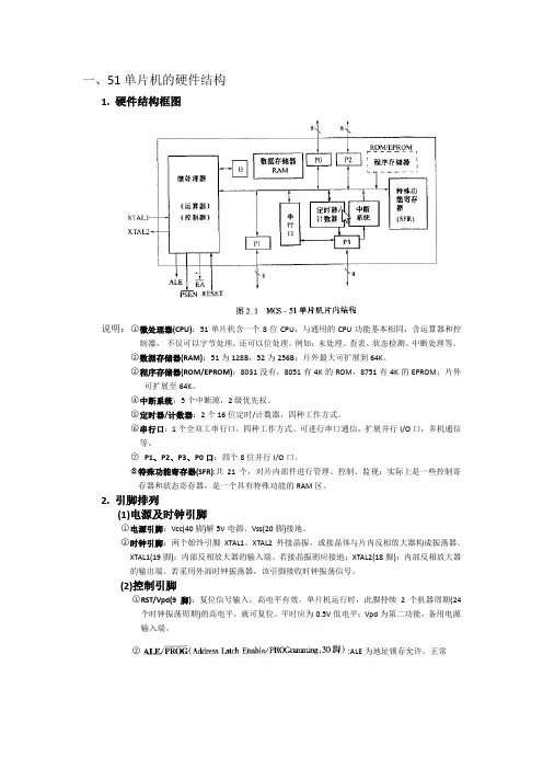
一、51单片机的硬件结构1. 硬件结构框图说明:○1微处理器(CPU):51单片机含一个8位CPU,与通用的CPU功能基本相同,含运算器和控制器,不仅可以字节处理,还可以位处理。
例如:未处理、查表、状态检测、中断处理等。
○2数据存储器(RAM):51为128B,52为256B;片外最大可扩展到64K。
○3程序存储器(ROM/EPROM):8031没有,8051有4K的ROM,8751有4K的EPROM;片外可扩展至64K。
○4中断系统:5个中断源,2级优先权。
○5定时器/计数器:2个16位定时/计数器,四种工作方式。
○6串行口:1个全双工串行口,四种工作方式。
可进行串口通信,扩展并行I/O口,多机通信等。
○7P1、P2、P3、P0口:四个8位并行I/O口。
○8特殊功能寄存器(SFR):共21个,对片内部件进行管理、控制、监视;实际上是一些控制寄存器和状态寄存器,是一个具有特殊功能的RAM区。
2. 引脚排列(1)电源及时钟引脚○1电源引脚:Vcc(40脚)解5V电源、Vss(20脚)接地。
○2时钟引脚:两个始终引脚XTAL1、XTAL2外接晶振,或接晶体与片内反相放大器构成振荡器。
XTAL1(19脚):内部反相放大器的输入端。
若接晶振则应接地;XTAL2(18脚):内部反相放大器的输出端。
若采用外部时钟振荡器,该引脚接收时钟振荡信号。
(2)控制引脚○1RST/Vpd(9脚):复位信号输入,高电平有效。
单片机运行时,此脚持续2个机器周期(24个时钟振荡周期)的高电平,就可复位。
平时应为0.5V低电平;Vpd为第二功能,备用电源输入端。
○2:ALE为地址锁存允许,正常工作时,ALE不断输出正脉冲信号。
当访问外部存储器时,ALE输出信号的负跳变沿用作低8位地址的锁存信号;PROG’为编程脉冲输入端。
○3PSEN’(Program Strobe Enable,29脚):程序存储器允许输出控制端。
低电平是外部程序存储器选通。
51单片机控制智能小车(毕业论文)目录前言方案设计与论证控制器模块选取电机模块选取电机驱动器模块选取电源模块选取硬件设计主控系统电机模块电机驱动模块电源模块按键模块软件设计直行设计转弯设计调试中存在的问题参考文献一、前言:随着汽车工业的迅速发展,关于汽车的研究也就越来越受人关注。
全国电子大赛和省内电子大赛几乎每次都有智能小车这方面的题目,全国各高校也都很重视该题目的研究。
可见其研究意义很大。
本设计就是在这样的背景下提出的,指导教师已经有充分的准备。
本题目是结合科研项目而确定的设计类课题。
我们设计的智能电动小车该具有圆形运行、三角形运行、矩形运行和三者一起运行的功能。
都是运行一循环自动停车。
根据题目的要求,确定如下方案:在现有玩具电动车的基础上,加了四个按键,实现对电动车的运行轨迹的启动,并将按键的状态传送至单片机进行处理,然后由单片机根据所检测的各种按键状态实现对电动车的智能控制。
这种方案能实现对电动车的运动状态进行实时控制,控制灵活、可靠,精度高,可满足对系统的各项要求。
本设计采用STC89C52单片机。
以STC89C52为控制核心,利用按键的动作,控制电动小汽车的轨迹。
实现四种运行轨迹。
STC89C52是一款八位单片机,它的易用性和多功能性受到了广大使用者的好评。
二、方案设计与论证控制器模块选取我们采用STC公司的STC89S52单片机作为主控制器,STC公司的单片机内部资源比起ATMEL公司的单片机来要丰富的多,它在5V供电情况下,最多支持80M晶振、且内部有512B的RAM数据存储器、片内含8k空间的可反复擦些1000次的Flash只读存储器、1K的EEPROM、8个中断源、4个优先级、3个定时器、32个IO口、片机自带看门狗、双数据指针等。
但是不兼容Atmel。
从方便使用的角度考虑,我们选择了此方案电机模块选取采用普通直流电机。
直流电机运转平稳,精度有一定的保证。
直流电机控制的精确度虽然没有步进电机那样高,但完全可以满足本题目的要求。

&&&&&&&&&&&&毕业设计(论文)题目:基于单片机的倒车雷达的设计学院:&&&&&&&&&&&专业:&&&&&班级:&&&&&&&学生:****导师:**** 职称:****起止时间:2014年3月3日至2014年6月15日毕业设计(论文)诚信声明书本人声明:本人所提交的毕业论文《基于单片机的倒车雷达的设计》是本人在指导教师指导下独立研究、写作的成果,论文中所引用他人的文献、数据、图件、资料均已明确标注;对本文的研究做出重要贡献的个人和集体,均已在文中以明确方式注明并表示感。
本人完全意识到本声明的法律后果由本人承担。
论文作者:(签字)时间:2014年6月10日指导教师已阅:(签字)时间:2014年6月10日西安邮电大学毕业设计(论文)任务书学生指导教师**** 职称****学院通信与信息工程学院专业信息工程题目基于单片机的倒车雷达的设计任务与要求1. 调研基于单片机的倒车雷达的设计的现状与背景。
2. 学习51单片机原理及超声波测距原理。
3. 进行相关模块功能的程序设计。
4. 在仿真软件上进行功能仿真。
5. 搭建硬件电路并调试。
6. 软件下载及综合调试。
7. 完成论文,准备答辩。
开始日期2014年3月3日完成日期2014年6月15日院长(签字) 201年 3 月7 日西安邮电大学毕业设计(论文) 工作计划2014年3 月10 日学生**** 指导教师**** 职称****学院通信与信息工程学院专业信息工程题目基于单片机的倒车雷达的设计工作进程主要参考书目(资料)(1)郭天祥. 新概念51单片机C 语言教程:入门、提高、开发、拓展全攻略[M].: 电子工业, 2009. 1.(2)周立功等. 增强型80C51单片机速成与实践[M]. : 航空航天大学, 2003.(7)亮. 跟我学51单片机(一)——单片机最小系统组成与I/O 输出控制[J]. 电子制作,2011, 1: 73-77.1.计算机一台2.硬件材料若干每周指导一次,主要解答学生问题,指导研究进度,并检查阅读资料笔记和仿真程序。
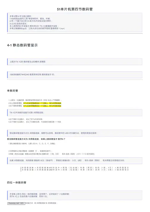
51单⽚机第四节数码管本笔记默认学习者已拥有:1.Keil5和stc 烧写⼯具 等各种软件、驱动、环境;2.有⼀个属于⾃⼰的 51单⽚机开发板及相关零件 ;3.认识C 语⾔的语法;本⼈使⽤的51开发板为 郭天祥C51 TX-1C 增强版开发板 ;本笔记根据B 站up 主:江科⼤⾃化协的教学视频 整理得到ヾ(•ω•)4-1 静态数码管显⽰上图为TX-1C 的 数码管及LED 模块 原理图138译码器和74HC245 都是⽤来控制 数码管显⽰ 的;单数码管1.上图为 ⼀位数码管,数码管有两种连接⽅式(对应 右边上下两幅图);2.右上图的原理图,8个LED的阴极都连在⼀个引脚上,称为共阴极连接;3.右下图的原理图,8个LED的阳极都连在⼀个引脚上,称为共阳极连接;TX-1C 开发板的连接⽅式是 共阴极连接;4.左下⾓的 左边图⽚ ,定义了8个LED的名称;5.左下⾓的 右边图⽚ ,定义了引脚的名称,与右图的引脚名称⼀⼀对应假设数码管连接⽅式为 共阳极连接,观察可以发现,数码管中的 LED 的引脚引出,使⽤的是就近原则;假设数码管连接⽅式为 共阴极连接,如果上数码管显⽰ 数字6 ?1.要让数码管显⽰ 数字6,让要 LED-A、C、D、E、F、G亮起;2.共阴极的公共端 要接地(给数据‘0’,或者是低电平);3.阳极(称为位选端)根据LED的亮灭需求给 数据0或1(1亮、0灭) ,称为 段码(阳码) (1011 1110 即为段码);如果 共阳极连接,共阳极端 要接到 VCC (⾼电平),阴极给 数据0或1 (1灭,0亮),称为 段码(阴码),和共阴极正好是相反关系;共阳极连接→共阳极端接VCC 并选中→阴极(位选端)传递(阴码)段码(1亮、0灭)→数码管显⽰共阴极连接→共阴极端接GND 并选中→阳极(位选端)传递(阳码)段码(1灭、0亮)→数码管显⽰四位⼀体数码管开发板上即为 四位⼀体的数码管,且有两个,正好组成了 ⼋位数码管;⽽TX-1C 上 包含的是六位数码管,⽽⾮⼋位;1.四位数码管 也有 两种连接⽅式,即 共阴极连接 和 共阳极连接 ;{Processing math: 100%2.四位数码管,(每位的公共端 单独引出来,位选端全部连在⼀起(所有A段连在⼀起、所有B段连在⼀起……),总共有12个引脚;假设数码管连接⽅式为共阴极连接,如何在第三位显⽰数字1 ?1.给第三位的公共端 赋值 0(低电平),给其他位的公共端 赋值 1(⾼电平);这样等同于 其他位的公共端(负极)接到了正极上,⽆论如何都亮不了;只有第三位能亮;2.这样给 LED-B、C 的位选端 赋值 1,其他 位选端 赋值0共阳极连接即为公共端赋值 1(⾼电平)亮,其他以此类推;3.发现这样⼀个现象,数码管⽆法在同⼀时间显⽰多个数字,其在同⼀时刻下只能有⼀个显⽰,只有⼀个数码管能被点亮,即使有多个被选中的数码管,显⽰的数字也是相同的;这种共⽤引脚的现象,是为了减少控制数码管IO⼝;(四位数码管有32个LED,如果都采⽤共阴极连接的⽅式,也要32+1(公共端)=33个引脚;)(采⽤这种链接,就只需要12个引脚即可控制四位数码管;)如何让数码管多位显⽰不同数字(动态数码管显⽰)?1.利⽤ ⼈眼视觉的暂留 和 数码管显⽰的余辉 的原理先让第⼀位数码管显⽰1,然后很快地让第⼆位数码管显⽰2,再很快地让第三位数码管显⽰3,让它不断地扫描,重复显⽰1、2、3的过程,这样三个数字就“同时”显⽰了;原理分析138译码器1.观察到 原理图右图 与数码管有关的,有138译码器(74LS138)和74HC245两枚芯⽚;TX-1C的原理图为左图,也有两个74HC573芯⽚与数码管有关;芯⽚名称与功耗、电压、说明符号有关,具体内容不做分析;2.如图,数码管连接⽅式为 共阴极连接,这样传输数据,就能让第三位显⽰ 数字1 了;3.⽽上⾯的 LED1 ~ 8,其实接在了138译码器的输出端,138译码器正好可以实现让LED1 ~ 8输出 0或1;LED1 ~ 8 对应了 TX-1C 六位数码管的SEG DS 1 ~ 6;4.138译码器可将LED 1 ~ 8的⼋个端⼝ 转化为 由 3个端⼝ (P22、P23、P24)控制,⽽G1、G2A、G2B端⼝ 被 称为 使能端;使能端相当于⼀种开关,如果电平有效,它就可以⼯作;如果电平⽆效,它就不⼯作;观察原理图发现,使能端是已经接好 VCC 和 GND 的,也就是说,其上电其实就会⼯作TX-1C的74HC573也是同理,但其并未压缩控制端⼝的数量;5.138译码器也叫“38线译码器”,是由3个线到8个线,其中C是⾼位、A是低位,CBA组成的数符合8进制,控制着Y0 ~ Y7 这8个端⼝;6.所以,138译码器的作⽤就是⽤来选中某⼀位数码管的74HC2451.74HC245是⼀种 双向数据缓冲器,VDD、GND都可视为电源,OE为使能(其 接地 就⼯作);2.DIR(direction),是⽅向的意思,它接到了VCC(⾼电平)上,将数据从左边输出到右边,从右边将数据读取回左边;DIR若接到低电平上,会将数据从右边输出到左边,从左边将数据读取回右边;3.单⽚机的⾼电平 驱动能⼒有限,其输出的最⼤电流不能太⼤;其低电平 驱动能⼒强;因此,LED模块才采⽤了低电平点亮的模式;4.如果⽤⾼电平 直接点亮 数码管,电流会很⼩,灯会很暗;所以其加⼀个缓冲器,缓冲器可以提⾼ 其驱动能⼒,如果直接将 数据 输出 给 数码管,数据就会被视为 驱动数据;现在增加了缓冲器,数据 就变成了 控制信号,控制信号 只需要很微弱,缓冲器 就可以接收到,缓冲器再通过⾃⼰接到的电源,输出 数据 到引脚上,这样控制的电流只需要⾮常⼩,就能驱动数码管 以⽐较亮的形式显⽰;2电容 是⽤来 稳定电源的,叫电源滤波;6.图右有 ⼀ 排阻,阻值为100R(即为100Ω),作⽤为 限流电阻 ,防⽌数码管的电流过⼤;TX-1C既没有电容,也没有排阻;原理总结1.⽤ 138译码器 使 数码管 的某⼀位 被选中;2.再给P0⼝⼀个 段码数据;TX-1C虽然⽤P0⼝控制段码输⼊,但也⽤P0⼝控制位选;需要先⽤ P2.6⼝和P2.7⼝控制输⼊数据是段码还是位选;P2.6⼝控制段码的输⼊;P2.7⼝控制位选的输⼊;例,给P2.6 数据1 (⾼电压)、给P2.7 数据 0 (低电压),就可以确定现在给数据是段码;1.由TX-1C的原理图可知,数码管内 LED灯 与 P0端⼝ 的顺序关系:(1)LED的名称定义是通⽤⽆疑的;(2)数码管本⾝的引脚名称不重要,重要的是 LED与哪个 P0 的 引脚 相连;2.由TX-1C的原理图可知, P0.0引脚 控制 数码管的最左位,P0.5引脚控制 数码管的最右位,剩余引脚是没有控制 数码管 位选 的作⽤的,哪个P0 的 引脚 控制 六位数码管的 哪位 很重要;代码实现静态数码管显⽰(让数码管第三位显⽰3).c#include<reg51.h>sbit D=P2^6; //段码⼝sbit W=P2^7; //位选⼝void main(){D=0;W=1;P0=0xFB;//1111 1011W=0;D=1;P0=0x4F;//0100 1111while(1);}下⾯写出了⼀个通⽤函数,可以让数码管在 第⼏个位置 显⽰ 哪个数#include<reg51.h>#define uchar unsigned charsbit D=P2^6;sbit W=P2^7;void NixieTube(uchar wei,uchar duan){ //NixieTube是数码管的英⽂uchar WEI,DUAN; //(Nixie是⼥⽔妖的意思)D=0;W=1;switch(wei){ //位选部分case 1:WEI=0xFE; break;case 2:WEI=0xFD; break;case 3:WEI=0xFB; break;case 4:WEI=0xF7; break;case 5:WEI=0xEF; break;case 6:WEI=0xDF; break;}P0=WEI;W=0;D=1;switch(duan){ //段码部分case 0:DUAN=0x3F; break;case 1:DUAN=0x06; break;case 2:DUAN=0x5B; break;case 3:DUAN=0x4F; break;case 4:DUAN=0x66; break;case 5:DUAN=0x6D; break;case 6:DUAN=0x7D; break;case 7:DUAN=0x07; break;case 8:DUAN=0x7F; break;case 9:DUAN=0x6F; break;case 10:DUAN=0x77; break; //Acase 11:DUAN=0x7F; break; //Bcase 12:DUAN=0x39; break; //Ccase 13:DUAN=0x3F; break; //Dcase 14:DUAN=0x79; break; //Ecase 15:DUAN=0x71; break; //Fcase 16:DUAN=0x80; break; //.}P0=DUAN;}void main(){NixieTube(3,3);while(1);}运⾏结果如下:4-2 动态数码管显⽰1.如果只是单纯让其显⽰完⼀个再显⽰⼀个,代码如下:#include<reg51.h>#define uchar unsigned charsbit D=P2^6;sbit W=P2^7;uchar Nixiewei[]={0,0xFE,0xFD,0xFB,0xF7,0xEF,0xDF};uchar Nixiecode[]={0x3F,0x06,0x5B,0x4F,0x66,0x6D,0x7D,0x07,0x7F,0x6F,0x77,0x7F,0x39,0x3F,0x79,0x71,0x80};//将两个switch改进为数组void NixieTube(uchar wei,uchar duan){D=0;W=1;P0=Nixiewei[wei];W=0;D=1;P0=Nixiecode[duan];}void main(){while(1){NixieTube(1,1);NixieTube(2,2);NixieTube(3,3);}}运⾏结果如下:2.这是⼀个数码管的常见问题,称为 数码管的消影 ;位选-->段选-->位选-->段选-->位选-->......在这⼀位的段选(输⼊段码)结束,进⾏下⼀位的位选时,很短的时间内,上⼀位的数据会串到下⼀位数据⾥⾯去;所以我们在段选和位选之间,增加⼀个 P0 清零的操作;动态数码管显⽰(数码管同时显⽰123).c#include<reg51.h>#define uchar unsigned charsbit D=P2^6;sbit W=P2^7;uchar Nixiewei[]={0,0xFE,0xFD,0xFB,0xF7,0xEF,0xDF};uchar Nixiecode[]={0x3F,0x06,0x5B,0x4F,0x66,0x6D,0x7D,0x07,0x7F,0x6F,0x77,0x7F,0x39,0x3F,0x79,0x71,0x80};void Delayms(unsigned int x){unsigned int j;for(;x>0;x--) for(j=110;j>0;j--);}void NixieTube(uchar wei,uchar duan){D=0;W=1;P0=Nixiewei[wei];W=0;D=1;P0=Nixiecode[duan];Delayms(1); //让数码管稳定显⽰,⽴刻清零会让数码管显⽰较暗P0=0; //清零操作}void main(){while(1){NixieTube(1,1);NixieTube(2,2);NixieTube(3,3);}}运⾏结果如下:相关知识1.在运⾏某些代码时,TX-1C的LED点阵模块会乱闪2.将左下⾓ DOT-OE旁的跳线帽 拔下来即可 断开LED点阵模块,3.拔下来的跳线帽不要乱丢,可以 只插⼀个脚放在原处,也可以妥善保管在其他地⽅上图即为拔下来的跳线帽1.此元件为电容;2.104的数量规则与 第⼆节 所讲的电容是相同的,其单位是pF1000pF=1nF, 1000nF=1uF, 1000uF=1000mF, 1000mF=1FF 是⼀个很⼤的单位,正常电容都是uF、nF级别的;超级电容能达到1 ~ 2 F,其⼀般作为备⽤电池;3.TX-1C的原理图上,电容的量都是直接⽤单位标记好的。
Release Notes for C518051 Development Tool KitsThis file contains release notes and last minute changes that are not found in theprinted m anuals.Information in this file, the accompany manuals, and soft ware isCopyright © Keil Software, Inc and Keil Elektronik GmbH.All rights reserved.Contents1What's New in C512Example Program s3Device Database™4Peripheral Simulation5Technical Support6Contact DetailsWhat's New in C51The following sections list the changes instituted in each release of the C51 toolset.C51 Version 9.00 Release[µVision4]▪This C51 release com es with the new µVision4 IDE.[New Supported Devices]▪Evatronix R8051XC(1 DPTR), R8051XC2(1 DPT R), R8051XC2(2DPT R), R8051XC2(8 DPTR), R8051XC2-A(1 DPT R), R8051XC2-A(2DPT R), R8051XC2-A(8 DPTR), R8051XC2-AF, R8051XC2-B(1 DPTR),R8051XC2-B(2 DPT R), R8051XC2-B(8 DPT R), and R8051XC2-BFdevices.▪Nordic nRFLU1P-F16and nRFLU1P-F32 devices.▪NXP P89LPC9361device.▪Silabs C8051F580, C8051F581, C8051F582, C8051F583,C8051F584, C8051F585, C8051F586, C8051F587, C8051F588,C8051F589, C8051F590, and C8051F591 devices.[Device Support]▪Corrected:device settings for Infineon XC888-6FF, XC888CM-8FF,XC888LM-6FF, XC886-6FF, XC866L-1FR, XC866L-2FR, XC866L-4FR, andXC864-1FRI devices.▪Corrected: device settings for Nordic Semiconductor nRF24E1,nRF24E2, nRF9E5, nRF24LU1, and nRF24LE1 devices.▪Added: debug support for NXP P89LPC9361 and P89LPC954 devicesin the LPC900 EPM Emulator/Programmer.▪Updated: LPC900 EPM flash programmer configuration dialog tosupport devices with 16 flash sectors.[CX51 Compiler]▪Corrected: constant folding of two negative array index values. Forexample:unsigned char arr[512];unsigned int i;i = arr[i-1-5]; // incorrect in C51 V8: arr[i-4] instead of arr[i-6]▪Corrected: when using the NOAREGS directive, complex arithmeticwith nested calls m ay create incorrect results. For exam ple:#pragma NOAREGSint result;extern char f(unsigned char idx);result = (f(1)*0x100+f(0)) - (f(3)*0x100+f(2)); // incorrect result. POP destroys value in ACCLX51 Linker/Locater]▪Corrected: when using OPTIMIZE(10) or above, there was a potentialthat common code blocks are called incorrectly. Therefore programs m ayhave operated incorrectly.[BL51 Linker/Locater]▪Corrected: when using RTX51 user interrupt functions wereoverlapping with RTX ISR vectors which resulted in a linker warning.▪Corrected: data overlaying may not work when the last input modulecontains an interrupt function; the linker incorrectly issues WARNING 16:main uncalled.C51 Version 8.18 Release[Device Support]▪Added: debug support for NXP P89LPC9408in the LPC900 EPMEmulator/Programmer.[New Supported Devices]▪Nuvoton W681308device.▪NXP P89LPC9201, P89LPC9211, P89LPC922A1, P89LPC9241,P89LPC9251, P89LPC9301, P89LPC931A1, P89LPC9331, P89LPC9341,and P89LPC9351 devices.▪Silabs C8051F500, C8051F501, C8051F504, C8051F505,C8051F506, C8051F507, C8051F508, C8051F509, C8051F510,C8051F511, C8051F700, C8051F701, C8051F702, C8051F703,C8051F704, C8051F705, C8051F706, C8051F707, C8051F708,C8051F709, C8051F710, C8051F711, C8051F712, C8051F713,C8051F714, and C8051F715 devices.[ULINK2 Support]▪Corrected: potential deadlock on ST uPSD targets with ULINK2solved.[Device Simulation]▪Corrected: Infineon XC800 simulation of the MDU was incorrectlyimplem ented.▪Corrected: For C8051F12x/F13x devices the EXFn and TOGnbehavior matches with latest inform ation from SiLABS.▪Added: simulation for Atmel AT89C51RE2. The second UART is nowavailable for the simulation.[CX51 Compiler]▪Corrected: initialization failed on far addresses when the object islocated with _at_. For example:#pragma VARBANKING O2unsigned char far array[65530] _at_ 0x150006;unsigned long x1 = (unsigned long)(array); // incorrect address stored in 'x1'.C51 Version 8.17a Release[Device Support]▪Added: debug support for the follow devices from Analog DevicesADE5166, ADE5169, ADE5566,ADE5569, ADE7166F16, ADE7166F8,ADE169F16, ADE7566F16, and ADE7566F8 in the ADI Monitor Driver.▪Added: debug support for NXP P89LPC9321 and P89LPC9351devices in the LPC900 EPM Emulator/Programmer.[Device Support]▪Added: Nuvoton devices in the device database.▪Corrected: Port Pin P2.2 is available (instead of P2.5) on NXPP89LPC917 devices. This is now reflected in the peripheral dialogs.▪Corrected: UART0 baudrate is now correctly displayed whenTim er2/3/4 is used as baudrate generator on SiLabs C8051F13xdevices.[Device Simulation]▪Corrected: sim ulation of Reset Source Register (RSTSRC) and SFRPage Control Register (SFRPGCN) for SiLabs C8051Fxxx devices.▪Corrected: handling of Automatic Page Control Enable (SFRPGCN)and Reset Source Register (RSTSRC) for SiLabs C8051Fxxx devices.▪Corrected: sim ulation of PLLLCK (PLL Lock Flag) for SiLabsC8051F12x/13x devices. PLLLCK is now set when PLL is configuredcorrectly and frequency is locked.▪Added: support for V: user-defined memory area for NXP 80C51MXdevices.▪Corrected: sim ulation issues with the Evatronix R8051XC peripheralsDMA and interrupt.[CX51 Compiler]Corrected: when two long operands are loaded from com plex arrays (each with object size bigger than 256 bytes), there was a potential register overwrite in register R0. The result of the long operation was in such cases incorrect.Example:struct s2 { unsigned int idx : 1; } s2;struct s { unsigned long l1; unsigned char a[256]; unsigned long l2; } xdata sarr[2];unsigned long l;void main (void) {l = sarr[s2.idx].l1 + sarr[s2.idx].l2; // incorrect result of long addition }[A X51 Macro A ssembler]▪Corrected: in NXP 80C51MX m ode, DATA, IDATA, and EDATA can beplaced to absolute addresses 0x7F0000 and above. This is now accepted.▪Added: ECRM directive that allows to expand generic CALLinstructions to ECALL for NXP 80C51MX devices.C51 Version 8.16a Release[CX51 Compiler]▪Corrected: when int num bers are multiplied and assigned to long, theresult is potential incorrect. This problem has been introduced in V8.15.▪Corrected: C51 _at_ problem with linker code packing fixed.[A X51 Macro A ssembler]▪Enhanced: for the NXP MX devices, CALL/JMP instructions areencoded to ECALL/JMP when needed..[Device Support]▪Added: ULINK and Infineon DAS (Device Access Server) support forthe XC864 device.▪Enhanced: Evatronix R8051XC XDATA Banking example optimized.▪Enhanced: Infineon XC800 startup code.▪Added: Support for Infineon XC864 including a Blinky example.▪Added: Syntek Semiconductors STK6031and STK6032devices todevice database.[Device Simulation]▪Added: for SiLABS C8051F360/1/2/3/4/5/6/7/8/9andC8051F410/1/2/3.C51 Version 8.15 Release[Cx51 Compiler]▪Corrected: interrupt functions com bined with NOINTVECTOR wherenot detected by the linker as new root and an incorrect linker warningwas reported.▪Corrected: when using Dallas 390 m ode with ROM(D512K) orROM(D16M), pdata arrays could not be located anywhere in m emory.▪Corrected: when using the XCROM directive in com bination withfunction pointers, constant initializations where omitted.▪Enhanced: long multiplication with two unsigned int/char argumentshas now a m uch higher performance.[Target Support]▪Added: support for the Infineon USCALE XC800 hardware via theInfineon DAS Client for XC800.[Device Simulation]▪Corrected: access to MACACC was not corrected simulated for SiLABSC8051F12x and C8051F13x devices.▪Added: device support and simulation for Infineon XC878.▪Added: simulation for new peripherals (Software Reset, RTC, DMA)on Evatronix R8051XC core.▪Added: xdata banking support for Evatronix R8051XC core.[LX51 Linker/Locater]▪Corrected: Linker Code Packing may com bine incorrectly blocks fromseveral code banks into common areas.[ULINK2 Support]▪Added: Debug and Flash-Programming support for NXP P89LPC952and P89LPC954.C51 Version 8.12 Release[Device Simulation]▪Added: device support and simulation for SiLABSC8051T600/1/2/3/4/5 and C8051T610/1/2/3/4/5/6/7.[Cx51 Compiler]▪Corrected: nested call with struct pointer arguments whereincorrectly processed.[LX51 Linker/Locater]▪Corrected: sfr16 definitions in assembly code and C source file maygenerate Warning L46: SFR SYMBOL HAS DIFFERENT VALUE.C51 Version 8.11a Release▪[Device Support]Added: support for Ram t ron VRS51L3072 and VRS51L3174.▪Added: support for Nordic Semiconductor nRF24LU1.[Device Simulation]▪Added: device support and simulation for SiLABS C8051F336,C8051F337, C8051F338, and C8051F339.▪Corrected: PORTx and PCA output pins on SiLABS C8051F12x d id notcorrectly update in simulation.C51 Version 8.10 Release▪[Device Support]Added: support for Megawin MPC82G516A and MPC82L54A.▪Enhanced: startup code for Infineon XC800 devices has nowselections for device variants. Infineon XC88x AC step devices requiresto set the device to VCO bypass m ode before PLL switching.▪Added: support for NXP P89V52X2.[Device Simulation]▪Corrected: simulation of MULRDY and OSCICL corrected for SiLABSC8051F3xx series.▪Enhanced: simulation of Evatronix R8051XC watchdog tim er withoptional prescaler. For details refer to Application Note 191: ToolchainExtensions for R8051XC Core.▪Corrected: DPTR simulation of Evatronix R8051XC; when 2 DPT Rwhere selected the auto-increm ent feature (DPC register) did not work.Two R8051XC devices are now in the device database: R8051XC (8DPTR) with simulation for 8 DPTR, R8051XC (2 DPTR) with simulationfor 2 DPTR.▪Corrected: SiLABS simulation for UART #1 had a problem with thetransmit interrupt bit (TI) when SFR page was set to 1.[Cx51 Compiler]▪Corrected: the MODC2 directive did not correctly save and restoremultiple DPTR registers on interrupt entry/exit.▪Corrected: Assem bler instructions inserted with #pragma ASMtrigger now register usage of all CPU registers and therefore avoidsregister clashes.▪Corrected: strcm p and strnc mp library functions changed fromsigned char to unsigned char com pare (ANSI requirement).▪Improved: detection of conflicting memory types when used incom bination with typedef's, for example:typedef char code CCHAR;typedef CCHAR xdata XCHAR; // generates now WARNING C185: different memory spaceCCHAR idata var2; // generates now WARNING C185: different memory space [LX51 Linker/Locater]▪Corrected: REMOVEDUNUSED did not correctly work with SROMsym bols and linker code packing.▪Corrected: debug sym bols of absolute bits generated in AX51 hadwrong offset.▪Corrected: segm ent locating with the LAST keyword generatedunnecessary m emory gaps when used with code banking.▪Corrected: when linker code packing is used, an address reference tofar variables with _at placem ent was wrong.[BL51 Linker/Locater]▪Corrected: segm ents with a AJMP instruction as last instructionwhere located at the end of a 2KB block which generated a linker error. [ULINK and ULINK2 Support]▪Corrected: Verify failed on µPSD devices when common segm entswhere located to code banks, but no bank 0 exists.C51 Version 8.09 Release[Device Simulation]▪Corrected: wrong timing of the Tim er 1 in the Infineon XC800devices.▪Corrected: clock cal culation of Infineon XC88x devices was incorrect.▪Corrected: Dallas D80C400 simulation did not correctly switch tocontiguous m ode.▪Added: Simulation for At m el AT89C51AC3.▪[Device Support]Corrected: when debugging Infineon XC800 Devices with the DASinterface data/idata variables where shown incorrect ly.▪[Target Debugging for A nalog Devices ADuC83x, A DuC84x, and ADE7xxx]Options - Project - Debug - Use: ADI Monitor Driver selects target driver for the Analog Devices ADuC834, ADuC84x, and ADE7xxx devices. This driver is now extended to support the 1-Pin Pod interface and the new ADE7xxx devices.[Monitor-51, Monitor-390]▪Corrected: potential communication problems with low-costUSB-COM adapters.[Cx51 Compiler]▪Corrected: a code generation problem with bit-field arrays when thearray index is a function return value.C51 Version 8.08a Release[Device Simulation]▪Corrected: the previous version had a delay when starting signalfunctions. This delay is now removed so that the startup behavior isidentical to releases before version 8.06.▪Corrected: the behavior of JBC instructions on I/O ports was not fullycorrect. JBC instructions now read the SFR register (Px) instead of theI/O port value (PORTx).[Cx51 Compiler]▪Corrected: integer promotion was m issing on com plex arithmeticwith char/unsigned char and multiplication or division.[A x51 Macro A ssembler]▪Enhanced: the _DATE2_ m acro is now defined also for the A51 andAX51 Macro Assembler.[uVision3 IDE]▪Corrected: potential crash in the project window on right mouse clickwhen no item was selected.[Device Support]▪Corrected: Peripheral display for Port 4 and Port 5 of the NXP89LPC952 device was m issing.▪Enhanced: on XC800 devices the dialog Project - Options - Debug- ULINK Settings - Disable interrupts during steps is implemented.This option disables interrupts during single-stepping and thereforeexecutes only instructions from the current function.▪Added support for Infineon TLE78xx series.▪Corrected: sim ulation for external interrupt inputs EINT0 and EINT1on Infineon XC800 devices.▪Corrected: debugger startup problem s with the Infineon DAS server.C51 Version 8.06 Release▪[Device Support]Infineon XC800 Devices: added debugging and flash programmingsupport for new Infineon XC800 devices (XC866-1FR, XC856) withULINK and Infineon DAS server.▪Enhanced: Infineon XC800 startup code START_XC.A51 V1.02 thatsupports pdata addressing (C51: USING PDATA VARIABLES ONINFINEON XC800).▪SST Sm artCards: added core features for device sim ulation.[Device Simulation]▪Corrected: interrupt vector for 2nd UART on Philips P89LPC952 wasincorrectly configured in simulator and target dialog.▪Enhanced: VTREG PPAGE is initialized to 0 on all Philips LPC900devices to allow simulation of MOVX @Ri without configuration.▪Corrected: a problem with AT89S8252 EEPROM simulation.▪Corrected: a problem with the baudrate generation on At m el deviceswith X2 feature (the baudrate was displayed incorrect).▪Corrected: a problem with code banking on Mentor M8051EW core. [Cx51 Compiler]▪Corrected: code that is not used (i.e. with m acros) is removed, evenwhen it creates other side effects.▪Corrected: unexpected error m essage for syntactical correctstatem ent.struct st2 { unsigned char uc1; unsigned char uc2; };struct st1 { struct st2 st2; unsigned char u1; unsigned char u2; };struct st1 st;void main (void) {(&st.st2)->uc1 = 0; // gives error, but should be Ok.}▪Corrected: library function toint did no flag values 0x3A - 0x40 asincorrect.[ULINK and ULINK2 Support]▪Added: support for ULINK2 for the Infineon XC800 and ST uPSDseries.▪Added: device support for Infineon XC886, XC888, and XC856.C51 Version 8.05 Release▪[Device Simulation for Infineon XC88x Series]Added device sim ulation for Infineon XC886 and Infineon XC888.▪[Device Simulation for Philips P89LPC952/954]Corrected: the two serial windows did not work for the Philips P89LPC952/954 devices.▪[Device Simulation for M8051EW]Corrected: when M8051EW features were enabled, it was not possible to debug non-banking applications.▪[Device Simulation for R8051XC]Enhanced: som e features were not covered in the first revision of the simulator.Now the simulator also takes care about peripheral timing, and write operations to code m emory.▪[LX51 Linker/Locater]Corrected: when using interbank call table optim ization (?B_RST_BANK != 0xFF), the linker was optimizing too much.▪[ULINK Driver for ST uPSD]Corrected: flash programming did not work for uPSD3422 devices.[Cx51 Compiler]▪Enhanced: C51 did issue an error when accessing struc t m emberswith s->member instead of s.member.▪Corrected: using multiple dummy assignm ents to rem ove unusedvariables m ay cause register overwrites.▪Corrected: potential code problems when increm enting far pointerswith long constants.void func (void) {unsigned int i;long far* entry;while(i) {i--; // increment missingentry += 1L; // due to 'far' pointer increment with 1L}}▪Corrected: potential problem on SmartMX, when using Optimize level8 or 9 without OBJECTADVANCED.#pragma MXPint xdata x;char xdata * xdata p;void f1 (char *);void f2 (char *);void main (void) { // uses CMPW instruction that affects 'Z' flagif (x == 0xFFFF) f1 (p); // MOVX A,Rx,@DPTR destroys 'Z' flagelse f2 (p); // and cannot be combined}C51 Version 8.04 Release[Cx51 Compiler]▪Enhanced: The Warning C259: pointer: different mspace is im provedand covers now also situations where an address value is assigned.▪New: The Warning C289: converting non-pointer to pointer is issuedwhen a integer value is assigned to a pointer.▪Corrected: A problem with the SRC file output is wrong withoptimized address values.▪Corrected: dummy read to MD3 was missing for int*int m ultiplicationwhen using the Infineon/Evatronix MDU.▪Added: Support for the SiLABS Arithmetic Accelerator (available inC8051F12x and F13x devices) in the far banking library.▪[Device Support for Evatronix/Cast R8051XC Core]Added com plete sim ulation and com piler support for the features of theR8051XC core. Detailed information is provided in Application Note 191: Toolchain Extensions for the R8051XC Core.▪[Device Support for Mentor M8051EW Core]Enhanced simulation support for the Mentor M8051EW memory extension features. It is now possible to sim ulate code banking and far m emory applications and the address of the The address of the extension corefeatures of the R8051XC core. Detailed information is provided in Application Note 171: Using M8051EW Memory Extension.▪[Device Support for Infineon XC800 Series]Added ULINK debugging support and DAS driver for new Infineon XC800 devices (XC886, XC888). Detailed information is▪[BL51 and LX51 Linker/Locater]Corrected: there might be incorrect WARNING L15: MULTIPLE CALL TO FUNCTION messages when using syntax: OVERLAY (* ! (func1, func2,func3,...)) to group more than just two functions.C51 Version 8.02 Release▪[uVision Debugger]Added peripheral simulation support and target debugging dialogs for the following devices:▪Atm el AT89C51RE2, AT89C51IE2, AT89C51CC03, AT8xC51SND1,AT89S8253, AT89LP2052, AT89LP4052▪Revised: Atm el AT89C5131/AT89C5131A(added TWI), AT8xC5132(added TWI, ADC)▪Philips P89LPC9102, P89LPC9103, P89LPC9107. P89LPC9221,P89LPC9311, P89LPC932A1, P89LPC938,▪Philips P89LPC9401/P89LPC9408 (without LCD Driver), P89LPC952,P89LPC964, P89LPC966▪Philips P89V660, P90V662, P89V664[LX51 Linker/Locater]Corrected a problem with code banking, the linker reported incorrectly error L124: BANK SWITCH MODULE INCORRECT.▪[Cx51 Compiler]Corrected a m acro expansion problem, array index calculations with negative offset, and far access to absolute m emory locations.▪[Target Debugging Support for Infineon XC800 Series]Added ULINK debugging support and DAS driver for new Infineon XC800 devices (XC886, XC888).▪[ULINK Driver for ST uPSD]Added new JTAG device ID's for ST uPSD3212, uPSD3312, and uPSD3422.C51 Version 8.01 Release▪[uVision Debugger]Added peripheral simulation support and target debugging dialogs for the following devices:▪Silicon Labs C8051F120, Silicon Labs C8051F121, Silicon LabsC8051F122, Silicon Labs C8051F123,▪Silicon Labs C8051F124, Silicon Labs C8051F125, Silicon LabsC8051F126, Silicon Labs C8051F127,▪Silicon Labs C8051F130, Silicon Labs C8051F131, Silicon LabsC8051F132, Silicon Labs C8051F133[P89LPC952 and MCB950 Board Support]Added support for Philips P89LPC95x device series.▪[A X51 Macro A ssembler]Corrected a problem with forward references in sym bols which generates an error m essage.▪[LX51 Linker/Locater - Code Packing]Corrected a potential problem with code packing when modules are translated with different optimization levels (less than 8) but the OBJECTADVANCED directive.▪[L51_BA NK.A51 - Code Banking Configuration File]Changed behavior of the ?B_RESTORE_BANK entry with ?B_MODE=0 to avoid glitches when using the RTX51 or RTX51 Tiny operating system together with code banking.▪[Cx51 Compiler]Version number changed for logistic reasons. No other changes com pared to V8.00.C51 Version 8.00 Release▪[uVision3 IDE]The µVision3 IDE contains several enhancem ents orrected: the device simulation covers now the latest timing specification for Dallas DS89C420, DS89C430, DS89C440, and DS89C450 devices. The tim er simulation was previously based on a older data book and therefore incorrect.[Device Simulation]▪Corrected: the device sim ulation c overs now the latest tim ingspecification for Dallas DS89C420, DS89C430, DS89C440, andDS89C450 devices. The tim er simulation was previously based on a olderdata book and therefore incorrect.▪[Target Debugging for A nalog Devices ADuC83x and ADuC84x]Options - Project - Debug - Use: ADI Monitor Driver selects target driver for the Analog Devices ADuC834 and ADuC84x devices. This driver directly connects via a serial COM interface to the on-chip Download/Debug Kernel of the ADuC device. No specific monitor or firmware is required. A detaileddocum entation is available in the Analog Devices ADuC83x/84x Download/Debug Driver User's Guide (..\C51\HLP\MonADI.CHM).▪[Support for Infineon XC866]Added complete support for new Infineon XC800 Device series including device simulation, ULINK driver, and MCBXC866 Evaluation Board support.▪Example projects are provided in thefolder ..\C51\Examples\Infineon XC866.▪Complete docum entation is available in the MCBXC866 User'sGuide(..\C51\HLP\MCBXC866.CHM) which also explains the ULINKdriver.▪[Support for ST uPSD34xx Series]Added com plete ULINK support for new ST uPSD34xx device series.[C Library]▪Corrected: on Dallas 390, 400, 5240, and 5250 devices tan (INF)generated a wrong return, and printf ("%f")did not print the floatingpoint value INF and NaN.▪Corrected: the return value of scanf and sscanf was just 0xFF insteadof -1 when no arguments where processed.▪Corrected: the library takes care about the changed behavior of theMem ory Accelerator on Dallas DS80C390 Rev. C.▪Corrected: on Dallas 390, 400, 5240, and 5250 devices m emmove inxdata m emory failed when source buffer is overlapping destinationbuffer.C51 Version 7.50a Release▪[LX51 Linker/Locater]Corrected: potential problem with Linker Code Packing that m ight causein-efficient operation or a MEMORY SPACE OVERLAY warning.▪Corrected: fixup error messages when using the REMOVEUNUSEDdirective.▪Corrected: when using L51_BANK.A51 the far m emory addressingused a wrong offset (-64KB). Instead of X:0x20000 the X:0x10000 wasaddressed.▪[BL51 Linker/Locater]The new BL51 Linker/Locater was by accident not included in Version 7.50.▪[C Library]Corrected a problem on Dallas 390, 400, 5240, and 5250 devices with log and log10 when const data is not in stored in segm ent 0 (C:0x0000-C:0xFFFF).C51 Version 7.50 Release▪[uVision2 Debugger]Added Extended Memory Simulation for Mentor M8051EW. Refer to Application Note 171: Using M8051EW Memory Extension in the folder \C51\EXAMPLES\M8051EW.Added peripheral simulation support and target debugging dialogs for the following devices:▪Dallas Semiconductor DS89C420,▪Dallas Semiconductor DS89C430,▪Dallas Semiconductor DS89C440,▪Dallas Semiconductor DS89C450,▪Silicon Labs C8051F000,▪Silicon Labs C8051F001,▪Silicon Labs C8051F002,▪Silicon Labs C8051F005,▪Silicon Labs C8051F006,▪Silicon Labs C8051F007,▪Silicon Labs C8051F010,▪Silicon Labs C8051F011,▪Silicon Labs C8051F012,▪Silicon Labs C8051F015,▪Silicon Labs C8051F016,▪Silicon Labs C8051F017,▪Silicon Labs C8051F350,▪Silicon LabsC8051F351,▪Silicon LabsC8051F352,▪Silicon LabsC8051F353,▪SST SST89E554RC,▪SST SST89E564RD,▪SST SST89V554RC,▪SST SST89V564RD.▪[ISD51 In-System Debugger]Added example configuration for Dallas DS89C420, DS89C430, DS89C440, and DS89C450 devices. For details refer to Application Note 177: Using ULINK with STMicroelectronics Turbo µPSD 3300/3400 Devices and the sam ple projects in the folder ..\C51\EXAMPLES\ST uPSD.[C51 Compiler]▪Corrected a code generation issue for negative array index values.For example:signed int i = v1 - v2;value = table [i + 4]; // code works for 'signed char' index// but fails with 'signed int' index▪Added MODC2 Compiler Directive: enables use of dual datapointers available on the Cast and Evatronix R80515 core. Usingadditional data pointers improves the performance of the followinglibrary functions: memcpy, memmove, memcmp, strcpy, andstrcmp.▪Added MODH2 Compiler Directive: enables use of dual datapointers available on Hynix, ST uPSD 33xx, and ST uPSD 34xx devices.Using additional data pointers improves the performance of the followinglibrary functions: memcpy, memmove, memcmp, strcpy, andstrcmp.▪[CX51 Compiler]Corrected the following problem s for the Sm artMX instruction set:▪Switch/case with long types and ROM(HUGE).▪Over optimization with CMPW instruction.▪Stack adjust m ent failure with setjmp/longjmp library routines.▪[C Library]Corrected several library problems including:▪Corrected a problem on Dallas 390, 400, 5240, and 5250 deviceswith asin, acos, and atan when const data is not in stored in segment 0(C:0x0000-C:0xFFFF).▪The labs function has been optimized and is now fully reentrant.▪Added configuration symbol ?C?DPSEL that defines DPSEL SFRaddress for MOD517(NOAU)multiple DPTR support. May be used forMentor M8051EW based devices which have the Infineon m ethod formultiple DPT R but with a different DPSEL SFR address. The ?C?DPSELdefinition shown below m ay be included in a chip-specific Startup.A51 file.Without this definition, the DPSEL register is accessed at the defaultaddress 0x92.PUBLIC ?C?DPSEL?C?DPSEL DATA 0A2H ; define DPSEL address for Mentor M8051EW▪[LX51 Linker]Added the REMOVEUNUSED(abbreviation RU) directive which removes unused program and data segm ents provided that Data Overlaying is enabled.▪[ULINK]Added instruction trace support to the STMicroelectronics uPSD ULINK Driver.For details refer to Application Note 177: Using ULINK with STMicroelectronics Turbo µPSD 3300/3400 Devices and the sam ple projects in the folder ..\C51\EXAMPLES\ST uPSD.▪[BL51/LX51 Linker]Improved the OVERLAY directive. Now, using OVERLAY (* ! (func1, func2)), you m ay com bine the segm ents of several function call trees. This is useful for interrupt functions that have overlayable data but use the sam e interrupt level.Such interrupt functions cannot interrupt each other. Therefore, data overlaying of both call trees is possible. For example:void irq0 (void) interrupt 0 {unsigned char arr[10];arr[0] = 0;}void irq1 (void) interrupt 1 {unsigned char arr[10];arr[0] = 0;}If irq0 and irq1 are set to the sam e priority level their data areas m ay be overlaid. The OVERLAY directive m ay be specified to do that as follows:BL51 ... OVERLAY (* ! (irq0, irq1))The linker map file shows the following OVERLAY MAP.SEGMENT DATA_GROUP+--> CALLED SEGMENT START LENGTH----------------------------------------------?PR?IRQ1?I 0008H 000AH*** NEW ROOT *********************************?PR?IRQ0?I 0008H 000AHNote that both functions' call trees are overlaid.C51 Version 7.20 Release▪[uVision2 Debugger]。

郭天祥十天学通单片机TX-1C单片机实验板所有课作业+答案,特别整理,供单片机爱好与学习者使用讲次内容细节第一讲学单片机预备知识、如何点亮一个发光管单片机能做什么,基本电子知识,如何用TX-1C单片机学习板学习单片机,C51 知识简介,如何申请免费芯片样品。
点亮一个发光管,第二讲流水灯设计、蜂鸣器发声、继电器控制简单延时程序、子程序调用、带参数子程序设计、流水灯同时蜂鸣器响、如何驱动蜂鸣器,及如何驱动继电器,集电极开路的概念及应用。
第三讲数码管显示的原理、数码管的静态显示共阳、共阴数码管显示原理、定时器工作方式介绍、重点讲述工作方式2、中断概念及中断函数写法、外部中断试验、定时器中断应用第四讲数码管的动态显示原理及应用实现动态扫描概念、定时器、中断加深用单片机的定时器及中断设计一个60 秒定时器第五讲独立键盘、矩阵键盘的检测原理及实现键盘用来做什么、如何键盘检测、消抖、键盘编码、带返回值函数写法及应用第六讲AD、DA 的工作原理及实现、运放电路模拟电压与数字电压的关系、为什么要使用AD 及DA、ADC0804 的操作方法、DAC0832 的操作方法第七讲串口通讯原理及操作流程串口通讯工作方式、10 位数据通讯、波特率概念、如何根据波特率计算定时器初值、串口打印在调试程序中的应用。
第八讲 1 602液晶、12864 液晶显示原理及实现最简单液晶工作原理、如何开始对一个没有任何概念的芯片开始单片机的操作第九讲IIC总线AT24C02芯片工作原理IIC总线工作原理、目前非常通用的一种通信机制第十讲利用51 单片机的定时器设计一个时钟综合运用51 单片机知识设计一个可以随意调节时间、带整点闹铃的时钟。
(其中用到定时器、中断、按键、蜂鸣器、数码管或串口通信)第^一讲用DS12C887时钟芯片设计一个高精度时钟DS12C887内部带有锂电池,系统掉电情况下可自行精确走10 年,并带有闹钟功能、年、月、日、时、分、秒等。
C51单片机知识总结C51单片机知识总结单片机I/O口的使用51单片机总共有P0、P1、P2、P3四个8位双向输入输出端口,每个端口都有锁存器、输出驱动器和输入缓冲器。
4个I/O端口都能作输入输出口用,其中P0和P2通常用于对外部存储器的访问。
在无片外扩展存储器的系统中,这4个端口的每一位都可以作为准双向通用I/O端口使用。
在具有片外扩展存储器的系统中,P2口作为高8位地址线,P0口分时作为低8位地址线和双向数据总线。
下图为P0口的某位P0.n(n=0~7)结构图,它由一个输出锁存器、两个三态输入缓冲器和输出驱动电路及控制电路组成。
从图中可以看出,P0口既可以作为I/O 用,也可以作为地址/数据线用。
①输出时CPU发出控制电平“0”封锁“与”门,将输出上拉场效应管T1截止,同时使多路开关MUX把锁存器与输出驱动场效应管T2栅极接通。
故内部总线与P0口同相。
由于输出驱动级是漏极开路电路,若驱动NMOS或其它拉流负载时,需要外接上拉电阻。
P0的输出级可驱动8个LSTTL负载。
②输入时----分读引脚或读锁存器读引脚:由传送指令(MOV)实现;下面一个缓冲器用于读端口引脚数据,当执行一条由端口输入的指令时,读脉冲把该三态缓冲器打开,这样端口引脚上的数据经过缓冲器读入到内部总线。
读锁存器:有些指令如:ANLP0,A称为“读-改-写”指令,需要读锁存器。
上面一个缓冲器用于读端口锁存器数据。
**原因:如果此时该端口的负载恰是一个晶体管基极,且原端口输出值为1,那么导通了的PN结会把端口引脚高电平拉低;若此时直接读端口引脚信号,将会把原输出的“1”电平误读为“0”电平。
现采用读输出锁存器代替读引脚,图中,上面的三态缓冲器就为读锁存器Q端信号而设,读输出锁存器可避免上述可能发生的错误。
**P0口必须接上拉电阻;在读信号之前数据之前,先要向相应的锁存器做写1操作的I/O口称为准双向口;三态输入缓冲器的作用:(ANLP0,A)准双向口:从图中可以看出,在读入端口数据时,由于输出驱动FET并接在引脚上,如果T2导通,就会将输入的高电平拉成低电平,产生误读。
单片机实训总结(实用版)编制人:__________________审核人:__________________审批人:__________________编制单位:__________________编制时间:____年____月____日序言下载提示:该文档是本店铺精心编制而成的,希望大家下载后,能够帮助大家解决实际问题。
文档下载后可定制修改,请根据实际需要进行调整和使用,谢谢!并且,本店铺为大家提供各种类型的实用范文,如工作计划、工作总结、演讲稿、合同范本、心得体会、条据文书、应急预案、教学资料、作文大全、其他范文等等,想了解不同范文格式和写法,敬请关注!Download tips: This document is carefully compiled by this editor. I hope that after you download it, it can help you solve practical problems. The document can be customized and modified after downloading, please adjust and use it according to actual needs, thank you!Moreover, our store provides various types of practical sample essays for everyone, such as work plans, work summaries, speech drafts, contract templates, personal experiences, policy documents, emergency plans, teaching materials, complete essays, and other sample essays. If you want to learn about different formats and writing methods of sample essays, please stay tuned!单片机实训总结单片机实训总结(通用3篇)单片机实训总结篇1《单片机》这门课程我已经学了一个学期了,在这一个学期的学习过程中,我一开始不怎么懂得编程,但慢慢的我现在已经不仅会读程序还会写程序了。
本问题与解答仅用于结合郭天祥51单片机学习板理解和应用方便,实际有些说法总结不一定正确或准确。
1、Int取值范围?(一句话16位,65536)单片机是8位机还是16位机?STC学习板单片机是8位的,一般单片机是几位的,他的字节也就是几位的,所以STC的字节应该是8位。
而字符一般是占用字节最少的数据类型,所以字符类型是8位,int类型一般是字符类型的2倍-16位,浮点数类型是4倍字符-32位,最长的是双精度的8倍字符,也就是64位。
总之,单片机是N位的,则单片机字符类型也是N位的,整型是2N位,浮点数是4N位。
其他围绕着三种类型来展开。
2、数码管显示锁存器的使用?(一句话存完数据再关闭即可)DULA WELA打开段选,打开位选,段选选哪个管,位选选单管数据。
应用流程:打开锁存,送入数据,关闭锁存。
举例:dula=1;P0=0xff;dula=0;(也可以送入数据后再打开锁存,打开后再关闭P0=0xff; dula=1;dula=0)备注:1、段选可以先送入P0=0XFF,这个是先关闭数码管显示,防止有乱码,也可以消影。
2、延时问题,通常0.1秒才可以开始分清数码管的数据。
动态显示时,通常是1ms左右延时。
再长可能会闪烁。
3、流水灯控制的两种方法?总线法、位操作法总线法:直接对P1口整体赋值。
比如P1=0x5f;位操作法:首先对P1口位定义,然后再赋值0或者1。
LED1=P1^0;LED1=1;4、11.0592晶振2种软件延时方法的时间精度问题?(一句话110为1毫秒)第一种:while(a--);这个a=1,就认为延时了0.01毫秒。
第二种:for(a=110,a>0,a--) 这个for执行完,就认为延时了0.25毫秒?原因:1个机器周期是12个时钟周期(1/11.0592微妙,1.08微秒),一条指令需要1-4个机器周期。
上面2个指令,执行一次正好需要一个机器周期,大约是12/11.0592微秒,1微秒多一些?实际运行时间规律不是太一致,根据调试经验,如果unsigned int型变量时,a=110,大约正好是1毫秒。
51单片机实验心得体会5篇(经典版)编制人:__________________审核人:__________________审批人:__________________编制单位:__________________编制时间:____年____月____日序言下载提示:该文档是本店铺精心编制而成的,希望大家下载后,能够帮助大家解决实际问题。
文档下载后可定制修改,请根据实际需要进行调整和使用,谢谢!并且,本店铺为大家提供各种类型的经典范文,如述职报告、演讲发言、汇报材料、对照材料、心得体会、策划方案、规章制度、教学资料、作文大全、其他范文等等,想了解不同范文格式和写法,敬请关注!Download tips: This document is carefully compiled by this editor. I hope that after you download it, it can help you solve practical problems. The document can be customized and modified after downloading, please adjust and use it according to actual needs, thank you!Moreover, our store provides various types of classic sample essays for everyone, such as job reports, speeches, presentation materials, reference materials, insights, planning plans, rules and regulations, teaching materials, complete essays, and other sample essays. If you want to learn about different sample formats and writing methods, please pay attention!51单片机实验心得体会5篇心得体会是内在世界的翻译,将情感的语言变为思考的文字,重视体会的写作,我们才能让自己的观点影响更多人,本店铺今天就为您带来了51单片机实验心得体会5篇,相信一定会对你有所帮助。
51单片机笔记经典2一、填空题1、A T89S51单片机为8位单片机,共有40个引脚。
2、M CS-51系列单片机的典型芯片分别为8031、8051、8751 。
3、A T89S51访问片外存储器时,利用ALE信号锁存来自P0 口发出的低8 位地址信号。
4、A T89S51的P3 口为双功能口。
5、A T89S51内部提供2个可编程的16位定时/计数器,定时器有4种工作方式。
6、AT89S51有2级中断,5个中断源。
7、AT89S51的P2 口为高8 位地址总线口。
8、设计一个以AT89C51单片机为核心的系统,如果不外扩程序存储器,使其内部4KB闪烁程序存储器有效,那么其EA*引脚应该接+5V9、单片机系统中使用的键盘分为独立式键盘和行列式键盘,其中行列式键盘的按键识别方法有扫描法和线反转法。
10、AT89S51内部数据存储器的地址范围是00H~7FH,位地址空间的字节地址范围是 20H~2FH ,对应的位地址范围是 00H~7FH ,外部数据存储器的最大可扩展容量是 64K 。
11、如果(A)=34H,(R7)=0ABH,执行XCH A, R7;结果(A)= 0ABH,(R7)=34H 。
12、在R7初值为00H的情况下,DJNZ R7, rel指令将循环执行256次。
13、欲使P1 口的低4位输出0,高4位不变,应执行一条ANL P1, #0F0H命令。
14、假设CPU使用的是存放器第1组,R0~R7的地址范围是08H-0FH。
15、单片机进行串行通信时,晶振频率最好选择11.0592MHz 16、当MCS-51执行MOVX A,@R1指令时,伴随着RD*控制信号有效。
17、假设A中的内容为67H,那么,P标志位为1。
18、AT89S51唯一的一条16位数据传送指令为MOV DPTR,data16。
19、LJMP的跳转范围是64K, AJMP的跳转范围是2KB,SJMP的跳转范围是土128 B〔或 256B〕。
1)二极管导通电流I:3mA-10mA;导通压降v:1.7V。
(排阻计算公式:R = VCC(5V)-v(1.7V)/I(3mA) )。
2)电源指示灯开关电源:内部有开关控制电流大小,不稳定。
去耦电容:稳压,去波。
3)锁存器(74HC573)OE:OutEnable,低电平有效(必须为低电平)。
输入端:OE(1),LE(11锁存端diola),D(D0(2)-D7(9),一般接P1^0-P1^7)。
输出端:Q(1Q-8Q)。
Z:高阻状态,非高非低电瓶。
LE:为高时,Q端与D同变换;为低电平时,Q端保持上次状态。
sbit LED00 = 0x80; //位指针;指针大小占一个字节;指针控制一个位的值;sfr LED0 = 0x80; //字节指针;指针大小占一个字节;指针控制一个字节的值;4)51库函数头文件:#include <intrins.h>函数:unsigned char _crol_(unsigned char c,unsigned char b);描述:The _crol_ routine rotates the bit pattern for the character c left b bits. This routine is implemented as an intrinsic function. The _crol_ routine returns therotated value of c.5) 蜂鸣器名称:b:基极;C:集电极;e:发射集;原理:e极发射电子;当b极接低电平时,ce导通,并且放大电流;当b接高电平时,ce截止。
JPFMQ接P3.6管脚。
分类:有源蜂鸣器;无缘蜂鸣器。
(源:震荡源)Proteus:buzzer-有源;sounder、speaker-无源。
端口电压:0.02v。
6) 数码管P0管脚:没有上拉电阻,所有有三态。
P1、P2、P3管脚:有上拉电阻,没有三态。
分类:共阴极;共阳极。
显示方法:静态,动态。
段选:P0.0-P0.7。
位选:P2.0-P2.7。
7)继电器接口:P3.7。
D4:引流二极管,防止断电烧坏电炉原件。
8)独立键盘K1-K4:P3.2-P3.5。
K5-K8:P1.4-P1.7。
独立键盘检测程序:#include <reg52.h>void main(){while(1){if(K1 ==0){delay(20);//大约延时10-20msif(K1 ==0){//确独立按键K1按下}}while(!K1);//确认为一次动作}}9)4*4矩阵键盘行线:P1.0-P1.3。
竖线:P1.4-P1.7。
优点:占用端口少,硬件电路简单。
缺点:编程较复杂。
矩阵键盘的检测方法:扫描法和线反转法。
程序实例:1)扫描法#include <reg52.h>#define uchar unsigned char#define uint unsigned intuchar i,j,temp_num,num =16;uchar code scan[]={0xfe,0xfd,0xfb,0xf7};//1111 1110 - 1111 0111uchar code coding[][4]={//扫描码0xee,0xde,0xbe,0x7e,0xed,0xdd,0xbd,0x7d,0xeb,0xdb,0xbb,0x7b,0xe7,0xd7,0xb7,0x77};uchar code num_code[]={0xc0,0xf9,0xa4,0xb0,//数码管0-16编码0x99,0x92,0x82,0xf8,0x80,0x90,0x88,0x83,0xc6,0xa1,0x86,0x8e,0xfe};void delay(uint k)//延迟函数{uint data i,j;for(i=0;i<k;i++){for(j=0;j<180;j++){;}}}void main(){P1 =0xff;while(1){P1 =0xf0;if(0xf0!= P1)//第一次检测{// delay(20); //消抖// P1 = 0xf0; //第二次检测// if(0xf0 != P1)//实践证明不必消抖也是可以的// {temp_num = num;for(i=0;i<4;i++){P1 = scan[i];for(j=0;j<4;j++){if(coding[i][j]== P1){num =4*i + j;break;}if(num != temp_num)break;}}//}P1 =0xf0;while(0xf0!= P1);//防止多次检测}P0 = num_code[num];P2 =0x7F;}}2)线反转法#include <reg52.h>#define uchar unsigned char#define uint unsigned intsbit P37 = P3^7;//继电器接口uchar code coding[]={0xee,0xde,0xbe,0x7e,0xed,0xdd,0xbd,0x7d,0xeb,0xdb,0xbb,0x7b,0xe7,0xd7,0xb7,0x77};uchar code num_code[]={0xc0,0xf9,0xa4,0xb0,0x99,0x92,0x82,0xf8,0x80,0x90,0x88,0x83,0xc6,0xa1,0x86,0x8e,0xfe};uchar Key =16;//表示按键编号void delay(uint m){uint k;while(--m){for(k=0;k<180;k++);}}uchar detection()//检测按键{uchar scan1,scan2,key_code,i;P1 =0xf0;scan1 = P1;if(0xf0!= scan1){// delay(30);// scan1 = P1;// if(0xf0 != scan1)// {P1 =0x0f;scan2 = P1;key_code = scan1 | scan2; //组合编码for(i=0;i<16;i++){if(key_code == coding[i]){Key = i;P37 =!P37;return i;}}// }// P1 = 0xf0; 去掉上面的return就可以,两种区别是:// while(0xf0 != P1);1)按下就显示;// 2)按下放开之后才显示.}elseP1 =0xff;return16;}void dispalyI(uchar i)//数码管显示函数{P2 =0x7f;P0 = num_code[i];}void main()P1 =0xff;while(1){detection();dispalyI(Key);}}10)中断、计时、计数1.中断源:1)两个外部中断源:INT0(P3.2),INT1(P3.3)。
(INT: interrupt)2)三个片内定时器:T0(外部计数P3.4),T1(外部计数P3.5),T2。
(Timer)3)一个串口中断请:TI/RI。
2.定时器控制寄存器TCONTF0/TF1(Timer Flag):定时器0/定时器1溢出中断申请标志位,=0未溢出,=1溢出申请中断,进入中断后自动清零。
TR0/TR1(Timer Running):定时器运行启动控制位,=0定时器停止运行,=1定时器启动运行。
IT0/IT1(Interrupt Trigger触发):外部中断请求触发方式选择位,=0外部中断低电平触发,=1外部中断负跳变触发。
IE0/IE1:外部中断申请标志位,=0没有外部中断,=1有外部中断。
3.定时器允许寄存器IE(Interrupt Enabled)EX0/EX1(Enabled eXternal):分别是外部中断INT0/INT1中断允许控制位,=0禁止中断,=1允许中断。
ET0/ET1(Enabled Timer):分别是片内计时器T0/T1中断允许控制位,=0,禁止中断,=1允许中断。
ET2:T2中断允许控制位。
EA:总中断控制位,=0禁止全部中断,=1允许中断。
4.中断优先级控制寄存器IP(Interrupt Priority)PX0/PX1(Priority eXternal):INT0/INT1优先级控制位,=0低优先级,=1高优先级。
PT0/PT1/PT2(Priority Timer):T0/T1/T2中断优先级控制。
PS1(Priority serial port):串口中断优先级控制位。
5.定时器方式寄存器TMOD常用工作方式:(M1,M0) = (0,1):16位定时器。
(M1,M0) = (1,0):8位自动重装定时器。
C/T:计数器/定时器选择位,=0定时,片内计数;=1片外计数(T0,T1)。
GATE门控制位:=0由TRx启动计数器/定时器(TRx=1启动);=1由TRx和INTx 共同启动(TRx=1,INTx=1启动)计数器/定时器。
6.interrupt m修饰符m:0—外部中断INT01—定时/计数中断T02—外部中断INT13—定时/计数中断T14—串口中断5—定时/计数中断T2外部中断过程:1)开启中断总开关EA = 1;//Enabled All2)开启外部中断INT0开关EX0 = 1;3)选择外部中断的中断触发方式IT0 = 1;//0低电平触发,1负跳变触发4)设定优先级PX0 = 1;//0低优先级,1高优先级5)声明外部中断函数void EexternInterrupt()interrupt 0 //0外部中断0{…}定时器/计数器发生过程:1.定时器/计数器选择:定时器和计数器都是片内16位计数内存工作,当作为计数器时,片内16位计数内存是对外部T0/T1引脚的矩形波进行计数;当做为定时器时,片内16位计数内存是对晶振产生的方波进行12分频后所得的方波进行计数;定时和计数是由定时器方式寄存器TMOD的C/T位进行选择的。
2.定时/计数溢出事件方法当片内16位计数内存溢出时则触发溢出事件,溢出事件的发生可以有定时/计数中断产生,也可由软件检测溢出标志位TFx位的值产生。
定时/计数中断程序过程:1)打开总中断开关EA = 1;2)打开计时器中断开关ET0 = 1;3)选择启动方式、计数/定时、计数方式TMOD = 0x01;//TR0启动,定时(片内计数),16计数方式4)计数内存高低位置初值TH0 = 0x01;TL0 = 0x01;5)启动计数/定时器TR0 = 1;6)声明中断函数void TimerInterrupt()interrupt 1{TH0 = 0x01;//重装计数内存TL0 = 0x01;…}定时/计数软件检测程序过程:1)选择启动方式、计数/定时、计数方式TMOD = 0x01;//TR0启动,定时(片内计数),16计数方式2)计数内存高低位置初值TH0 = 0x01;TL0 = 0x01;3)启动计数/定时器TR0 = 1;4)软件检测TFx标志位While(1){if(TF0 == 1){TF0 =0;//必须手动清零TH0 = 0x01;//重装计数内存TL0 = 0x01;…}}精品文档精品文档。