Ef?cient FPGA Implementation of H.264CA VLC
Entropy Decoder
Ali Siblini?,Elias Baaklini?,Hassan Sbeity?,Ahmad Fadlallah?and Smail Niar?
?Lebanese University,Beirut,Lebanon
Email:ali.siblini@https://www.doczj.com/doc/8d18810353.html,.lb
?Arab Open University,Beirut,Lebanon
Email:{hsbeity,afadlallah}@https://www.doczj.com/doc/8d18810353.html,.lb
?University of Valenciennes,France
Email:{elias.baaklini,smail.niar}@univ-valenciennes.fr
Abstract—Multiprocessor-system-on-a-chip(MPSoC)is the dominating architecture in embedded systems.Applications need to be multi-threaded to bene?t from the concurrency provided by the MPSoC.Many parallel versions of the new emerging H.264/A VC[1]already exist.However,providing a full parallel H.264version is blocked by the fact that all parts of the decoder depend on the?rst sequential stage of the decoding process which is the entropy decoder(mainly CA VLC).The entropy decoder consumes about30%[8]of the total time of the decoder.In this work,we propose an optimized FPGA design achieving the demands of multi-threaded H.264decoder versions which can be integrated in an MPSoC.We focus in our work on time optimization and on cycle number decrease when decoding an encoded4x4block of pixels.We also aim to achieve a design that operates at high frequencies.The work leads to the ability to decode at least62frames per second for HD resolution1280x720. Decoding takes22clock cycles for one block of4x4pixels at most.The design has an upper frequency limit of247MHz.High resolutions frames such as1920x1088FHD(full high de?nition) video maintain a minimum frequency of30fps.
Keywords-FPGA,CALVC,Entropy Decoding,H.264,Video Decodin,Multi-Core,Embedded Systems
I.I NTRODUCTION
Multimedia hand-held devices are nowadays an essential element in our daily life.Smart phones devices are equipped in general with high de?nition screens and fast multi-core processors.Video decoding algorithms are becoming more complex in order to achieve better compression for high de?nition videos.H.264is currently one of the most widely used video compression standards for capturing,compressing, and broadcasting high de?nition videos.H.264offers better compression and better quality at the expense of higher algorithm complexity[1].
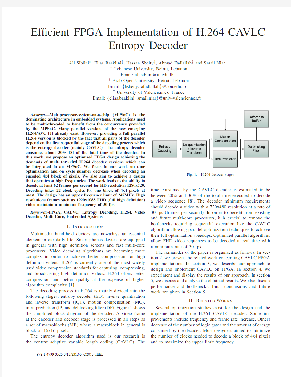
The decoding process in H.264is mainly divided into the following stages:entropy decoder(ED),inverse quantization and inverse transform(IQT),motion compensation(MC), intra-prediction(IP)and deblocking?lter(DF).Figure1shows the simpli?ed block diagram of the decoder.A video frame at the encoder and decoder stage is processed in all steps as a set of macroblocks(MB)where a macroblock in general is block of16x16pixels.
The entropy decoder algorithm used is our research is the context adaptive variable length coding(CA VLC).
The
Fig.1.H.264decoder stages
time consumed by the CA VLC decoder is estimated to be between20%and30%of the total time executed to decode a video sequence[8].The decoder minimum requirements should decode a video with a720x480resolution at a rate of 30fps(frames per second).In order to bene?t from existing and future multi-core processors,it is crucial to remove the bottlenecks requiring sequential execution like the CA VLC algorithm allowing parallel optimization techniques to achieve their full optimization speedups.Optimized parallel algorithms allow FHD video sequences to be decoded at real time with a minimum rate of30fps.
The remainder of the paper is organized as follows.In sec-tion2,we present the related work concerning CA VLC FPGA implementations.In section3,we describe our approach to design and implement CA VLC on FPGA.In section4,we experiment and display the results of our approach.In section 5,we discuss and analyze the obtained results.We also discuss performance and bottlenecks.Final conclusions and future work are given in Section5.
II.R ELATED W ORKS
Several optimization studies exist for the design and the implementation of the H.264CA VLC decoder.Some im-provements include frequency and frame rate increase.Others decrease of the number of logic gates and the amount of energy consumed by the decoder.Most designers aimed to minimize the number of clocks needed to decode a block of4x4pixels and to maximize the upper limit frequency.
978-1-4799-3525-3/13/$31.00 ?2013 IEEE
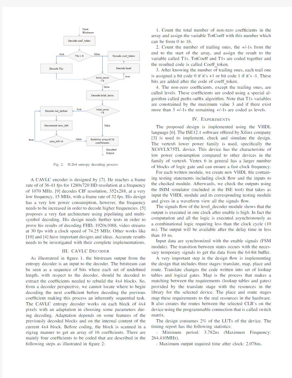
Fig.2.H.264entropy decoding process
A CA VLC encoder is designed by[7].He reaches a frame rate of of36-41fps for1280x720HD resolution at a frequency of1070MHz.[9]decodes CIF resolution,352x288,at a very low frequency,15MHz,with a frame rate of32fps.His design has a very low power consumption,however,the frequency needs to be increased in order to decode higher frequencies.[5] proposes a very fast architecture using pipelining and multi-symbol decoding.His design needs further tests in order to prove his results of decoding FHD,1920x1088,video streams at30fps with a clock speed of74.25MHz.Other works like [10]and[4]have important designs and ideas.Accurate results needs to be investigated with their complete implementations.
III.CAVLC D ECODER
As illustratred in?gure1,the bitstream output from the entropy decoder is an input to the decoder.The bitstream can be seen as a sequence of bits where each set of unde?ned length,with respect to the decoder,should be decoded to extract the coef?cients needed to rebuild the4x4blocks.So, from a decoder perspective,we cannot locate where to begin decoding the next coef?cient before decoding the previous coef?cient making this process an inherently sequential task. The CA VLC entropy decoder works on each block of4x4 pixels with an adaptation in choosing some parameters dur-ing decoding.Adaptation depends on some features of the previously decoded blocks and on the internal content of the current4x4block.Before coding,the block is scanned in a zigzag manner to get an array of16coef?cients.There are mainly four coef?cients to be coded that are described in the following steps as illustrated in?gure2:
1.Count the total number of non-zero coef?cients in the array and assign the variable TotCoeff with this number which can be from0to16.
2.Count the number of trailing ones,the+/-1s from the end to the start of the array,and assign the result to the variable called T1s.TotCoeff and T1s are coded together and the resulted code is called Coeff token.
3.After knowing the number of trailing ones,each trail one is assigned a bit code0if it’s+1or bit code1if it’s-1.These bits are added after the code of coeff token.
4.The non-zero coef?cients,except the trailing ones,are called levels.These coef?cients are coded using a special al-gorithm called pre?x-suf?x algorithm.Note that T1s variables are constrained by the maximum value3and if there exist more than3+/-1s the remaining+/-1s are coded as levels.
IV.E XPERIMENTS
The proposed design is implemented using the VHDL language[6].The ISE12.1software offered by Xilinx company [3]is used to implement,check and simulate the design. The vertex6lower power family is used,speci?cally the XC6VLX75TL device.This device has the characteristic of low power consumption compared to other devices in the family of vertex6.Vertex6in general has a larger number of blocks of logic gate and can ensure a fast clock frequency. For each written module,we create new VHDL?le contain-ing testing statements including clock?ow and the inputs to the checked module.Afterwards,we check the outputs using the ISIM simulator(included in the ISE tool)that takes as input the VHDL module and its corresponding testing module and gives in a waveform view all the signals?ow.
The signals?ow of the level decoder module shows that the output is executed in one clock after enable is high.In fact the computation and all the logic is executed asynchronously as a combinational logic requiring less than the clock cycle(10 ns).The output will be available after the delay time in less than10ns.
Input data are synchronized with the enable signals(FSM module).The transition between states occurs with the neces-sary temporary signals to get the data from the64-bit buffer.
A very important step in the design?ow is implementing the design that includes three stages:translate,map,place and route.Translate changes the code written into set of lookup tables and logical gates.Map is the process that makes a matching between the requirements(lookup tables and gates) provided by the translate stage with the resources in the library for the selected device.The place and route stages map these requirements to the real resources in the hardware. It also creates the routes between the selected CLB’s on the device using the programmable connection that is called switch matrix.
The design consumes2%of the LUTs of the device.The timing report has the following statistics:
-Minimum period: 3.782ns(Maximum Frequency: 264.410MHz).
-Maximum output required time after clock:2.078ns.
Fig.3.H.264CA VLC cycle results
TABLE I
C YCLES AN
D FRAM
E RATE O
F THE CAVLC ENTOPY DECODER-W ORST
C ASE S CENARIO
Format Resolution CA VLC cycles Frame cycles fps
VGA640x4804224001408000187.5
HD1280x7201267200422400062.5
FHD1920x10882872320957440027.6
-Maximum combinational path delay:1.121ns.
V.D ISCUSSION
Experiments are conducted using the worst case and the averaged case scenarios.The worst case scenario is when we have a block of16nonzero coef?cients that consume the maximum number of clocks given by the following equation: Maximum Clocks=T1+(level num*T2)+T3+(run num *T4)+Tm+2Where:T1is the number of clocks consumed by Totcoeff T1decoder module,T2is the number of clocks consumed by level decoder module,T3is the number of clocks consumed by total zeros module,T4is the number of clocks consumed by run before module,Tm is the number of clocks consumed for merging levels and run before zeros. Then maximum number of clocks is22clock cycles.So if we are to check the performance of the design with respect to the requirements considering the worst case scenario,clocks consumed to decode an HD frame of1280x720pixels is 4224000clocks as displayed in table1.However,a4x4block requires13cycles on average.Thus,the to total number of clocks to decode a slice decreased signi?cantly to2496000 clocks,achieving a frame rate of105fps with a clock frequency of264MHz.
The lowest frame rate to decode a FHD frame,1920x1088, is27.6fps.However,if we consider the average case,the rate increases to46.7fps.So a frame rate of30fps is reached with a87.4%possibility when decoding a FHD video sequence using our CALVC design.
TABLE II
C YCLES AN
D FRAM
E RATE O
F THE CAVLC ENTOPY DECODER-A VERAGE
C ASE S CENARIO
Format Resolution CA VLC cycles Frame cycles fps
VGA640x480249600832000317.3
HD1280x7207488002496000105.8
FHD1920x10881697280565760046.7
TABLE III
B IT RATES OF THE CAVL
C ENTOPY DECODER-W ORST C ASE S CENARIO
Format Resolution CA VLC bits Frame bits Kbps at30fps VGA640x480890880029696000989.9
HD1280x72026726400890880002969.6
FHD1920x1088605798402019328006731.1
TABLE IV
B IT RATES OF THE CAVL
C ENTOPY DECODER-A VERAGE C ASE
S CENARIO
Format Resolution CA VLC bits Frame bits Kbps at30fps VGA640x480614400204800068.3
HD1280x72018432006144000204.8
FHD1920x1088417792013926400464.2
VI.CONCLUSION AND FUTURE WORK
We have design and implemented a CA VLC for the H.264 entropy decoder on FPGA.Experiments show a high frame rate for HD and FHD video resolutions.Our future work focuses on implementing a complete H.264decoder on FPGA and on improving the overall performance of the decoder for consistent real time FHD execution.
R EFERENCES
[1]AISO/IEC.International standard.Part10:Advanced video coding,
14496-10,2003.
[2]K.Suehring.H.264reference software.http://bs.hhi.de/suehring/tml/.
[3]Xilinx Company.https://www.doczj.com/doc/8d18810353.html,l/.
[4]R.Osorio,J.Bruguera.An FPGA architecture for CABAC decoding in
manycore systems.In International Conference on Application-speci?c Systems,Architectures and Processors,pages293–298,2008.
[5]Tony Gladvin George,N.Malmurugan.The Architecture of Fast H.264
CA VLC Decoder and its FPGA Implementation.In Proceedings of the Third International Conference on International Information Hiding and Multimedia Signal Processing(IIH-MSP2007)-Volume02,pages389–392,2007.
[6]IEEE Standard VHDL Language Reference Manual.In IEEE Std1076,
2000.
[7]Zhibin Xiao,Bervan Baas A high-performance parallel CA VLC encoder
on a?ne-grained many-core system.In IEEE International Conference on Digital Object Identi?er,ICCD.2008,pages248-254,2008. [8] E.Baaklini,H.Sbeity,S.Niar,N.Amaneddine.H.264Color Com-
ponents Video Decoding Parallelization on Multi-core Processors.In 13th Euromicro Conference on Digital System Design:Architectures, Methods and Tools,DSD’10,pages785-790,2010.
[9]Sung-Kyu Choi,Jong-Gu Jeon,Woo-Sung Shim,Won-Kap Jang,Victor
H.S.Ha.Design and implementation of H.264-based video decoder for
digital multimedia broadcasting.In IEEE International Conference on Multimedia and Expo,ICME’04,pages149-152V ol.1,2004. [10]T.Lindroth,N.Avessta,J.Teuhola,https://www.doczj.com/doc/8d18810353.html,plexity Analysis
of H.264Decoder for FPGA Design.In IEEE International Conference on Multimedia and Expo,ICME’06,pages1253-1256,2006.
#include
基于proteus篮球计时计分器(史上最牛,含详细程序) #include
0x7f,0x6f,0x00}; uchar munite; //比赛剩余分位数 uchar second; //比赛剩余秒位数 uchar part; //当前比赛的节次 uchar s24; //24秒标志 uchar red_mark; //红队得分 uchar blue_mark; //蓝队得分 uchar key_move; //设置位移动 uchar key_red_add; //红队得分增加1 uchar key_red_mul; //红队得分减少1 uchar key_blue_add; //蓝队得分增加1 uchar key_blue_mul; //蓝队得分减少1 uchar key_pause; //暂停 uchar key_reset; //24秒复位及进入下一节复位 uchar time_tick1,time_tick2; uchar station; //状态标志位 uchar flag; //跳亮标志位 uchar talk1,talk2,num,num1; //报警信号标志 /*******函数声明********/ void init(); void init_timer(); void init_extra(); uchar key_scan(); void scanf(uchar p,uchar tw,uchar m,uchar s,uchar r,uchar b); void scanf1(uchar p,uchar r,uchar b); void scanf2(uchar tw,uchar r,uchar b); void scanf3(uchar m,uchar r,uchar b); void scanf4(uchar s,uchar r,uchar b); void play24(); void playstop1(); void playstop2(); /*********延时程序,t=1时,延时1ms************/ void delay(uchar t) { int i,j; for(j=0;j 单片机课程设计报告 篮球比赛计分器设计 姓名: 学号: 专业班级: 指导老师: 所在学院: 年月日 摘要 本设计是采用单片机AT89C52作为本设计的核心元件。利用7段共阴LED 作为显示器件。在此设计中共接入了8个7段共阴LED显示器,其中4个用于记录AB队的分数,每队2个LED显示器显示范围可达到0~99分,足够满足赛程需要,另外4个LED显示器则用来记录赛程时间,其中2个用于显示分钟,2个用于显示秒钟。赛程计时采用倒计时方式。即比赛前将时间设置好,比赛开始时启动计时,直至计时到零为止。计时范围可达到0~99分钟,也完全满足实际赛程的需要。当比赛队A对得1分时,按下A+1键;得2分时,按下A+2键;得3分时,按下A+3键;当加分出现错误时,可以按A-1键减1分,可以达到调整分数的作用;依照同样的方法可以记录B对的得分。 采用单片机控制使这个系统按键操作使用简洁,LED显示,安装方便。解决了篮球比赛计分器的安装问题,节约了线材,适合在各种规模的体育场馆使用,完全可以代替传统的用钟表进行计时的方法,当然稍加改动也可以用于其他球类比赛,是体育器材向智能化发展的一个实例。 本设计可以实现:1、能记录整个赛程的比赛时间,并能修改比赛时间 2、能随时刷新甲、乙两队在整个过程中的比分 3、中场交换比赛场地时,能交换甲、乙两队比分的位置 4、比赛结束时,能发出报警声,等功能 1 概述 3 1.1设计意义 (3) 1.2设计内容 (4) 1.3设计任务和要求 (4) 2 系统总体方案及硬件设计 4 2.1AT89C52简介 (4) 2.2数码管显示原理 (6) 2.3总体方案: (7) 2.4硬件原理图: (8) 3 软件设计 7 3.1主流程图: (7) 4.PROTEUS软件仿真8 5、课程设计体会10 附1:源程序代码11 附2 系统原理图21 《数字电子技术》课程设计题目:篮球比赛记分器设计 学院:信息科学与技术学院 专业:电子信息工程 班级:2010级(2)班 姓名:马慧2010508121 张驰2010508125 2012年7月6日 篮球比赛记分器设计 一、设计内容与要求: 设计一个篮球比赛记分显示器 基本要求: (1)电路具有加1分、加2分、加3分功能。 (2)电路具有减分功能。 (3)显示总分功能,用三位LED显示器,最高可现实999。 (4)每次篮球比赛后显示器可清零。 二、设计方案 对应篮球比赛规则的系统的要求,篮球记分有1分、2分、3分的情况,通过对电路输入一个脉冲、两个脉冲、三个脉冲,使计数器对分数进行统计,这需要三个脉冲分路。 电路要具有计分、减分及显示的功能。当球队比赛得分时,用加法计分器通过控制分路加相应的分数。如果裁判误判了,可用减法计数器减掉误判的分数。用三片计数器和三个半导体数码LED进行对分数的统计和显示。 电路框图 记分电路 加 减 置 换 二 分 脉 冲 显 示 显 示 分 数 清 零 一分脉冲三分脉冲 三、电路的设计 1、记分部分 设计要求记分部分包括加减两部分,故考虑双时钟输入的十进制计数器74LS192。74LS192是同步十进制可逆计数器,为双时钟输入,具有同步清零和同步置数等功能,具体功能表如下: 故计分部分电路设计如下: 2、显示部分 数码管按照其发光二极管的连接方式不同,可分为共阳极和共阴极两种。共阴极是指数码管中所有发光二极管的阴极连在一起接低电平,而阳极分别由a、b、c、d、e、f输入信号驱动,当某个输入为高电平时,相应的发光二极管点亮;共阳极数码管则相反,它的所有发光二极管的阳极连在一起接高电平,而阴极分别由a、b、c、d、e、 篮球计分器F P G A附 程序 单片机接口实验 篮球计分器的设计 姓名: 苗茂宇 班级: 14级12班 学号: 1408202007 导师: 党选举 专业: 控制科学与工程 成绩评定 目录 摘要 (1) Abstract (1) 1. FPGA及系统设计概述 (2) 1.1. EDA简介 (2) 1.1.1. EDA定义 (2) 1.1.2. EDA发展概述 (2) 1.1.3. HDL概述 (3) 1.1.4. 总结 (4) 1.2. FPGA简介 (4) 1.2.1. FPGA概述 (4) 1.2.2. FPGA原理 (5) 1.3. LCD1602 (6) 1.4. 产品现状及发展 (7) 1.5. 总体设计要求 (8) 1.5.1. 设计流程 (8) 1.5.2. 设计要求 (8) 1.6. 本章小结 (8) 2. 实验方案设计 (9) 2.1. 分频模块 (9) 2.2. 计时模块 (10) 2.3. 24秒计时模块 (12) 2.4. 计分模块 (14) 2.5. lcd驱动模块 (15) 2.6. 本章小结 (22) 3. 实验结论 (22) 4. 结束语 (23) 参考文献 (24) 附录 1 (25) 摘要 FPGA(现场可编程逻辑器件)以其体积小、功耗低、稳定性高等优点被广泛应用于各类电子产品的设计中。FPGA是基于硬件可编程的器件,设计者需要掌握硬件描述语言,Verilog HDL就是一种硬件描述语言。Verilog HDL语言是在C语言的基础上发展而来的,语法结构上与C语言有很多相似之处,继承了C语言的语法结构,但是其与C语言有着本质上的区别。本设计是基于FPGA 的篮球计时计分系统的设计,结合篮球比赛的实际过程,对系统进行了模块化设计,最终组合调试。硬件实验表明本系统计时计分准确,实时性好,能够很好的反应比赛进度,此次设计达到了设计预期。 关键词:FPGA;Verilog HDL;计时计分;模块化 Abstract FPGA (field programmable logic device) with its small size, low power consumption, high stability has been widely used in various types of electronic products design. FPGA is a programmable device based on hardware, designers need to master the hardware description language, Verilog HDL is a hardware description language. Verilog HDL language is developed on the basis of C language, grammar structure and C language have many similarities, inherited the grammar structure of C language and C language, but there's a difference between. This design is the design of FPGA basketball timing and scoring system based on the actual process, combined with the game of basketball, the system of modular design, the final assembly debugging. Hardware experiments show that the system timing accuracy, good real-time performance, can very good response competition schedule, the design achieves the expected design. Keywords: FPGA;Verilog HDL ; timing and scoring; modular 目录 第一部分设计任务与调研 (3) 第二部分设计说明 (5) 第三部分设计成果 (10) 第四部分结束语 (15) 第五部分致谢 (17) 第六部分参考文献 (18) 第七部分附录 (19) 第一部分设计任务与调研 一、调研 体育比赛记分系统是对体育比赛过程中所产生的比分等数据进行快速采集记录,加工处理,传递利用的信息系统。根据不同运动项目的不同比赛规则要求,体育比赛的记分系统包括测量类,评分类,命中类,制胜类得分类等多种类型。 比如篮球比赛是根据运动队在规定的比赛时间里得分多少来决定胜负的,因此,篮球比赛的记分系统是一种得分类型的系统。篮球比赛的记分系统由计分器等多种电子设备组成,同时,根据目前高水平篮球比赛要求,完善的篮球比赛记分系统设备应能够与现场成绩处理,现场大屏幕,电视转播车等多种设备相联,以便实现高比赛现场感,表演娱乐观众等功能目标。 由于单片机的集成度高,功能强,通用性好,特别是它具有体积小,重量轻,能耗低,价格便宜,可靠性高,抗干扰能力强和使用方便等独特的优点,使单片机迅速得到了推广应用,目前已经成为测量控制应用系统中的优选机种和新电子产品的关键部位。世界各大电气厂家,测控技术企业,机电行业,竞相把单片机应用于产品更新,作为实现数字化,智能化的核心部件。篮球计时计分器就是以单片机为核心的计时计分系统,由计时器,计分器,综合控制器和24秒控制器等组成。 二、设计任务 (1)给甲、乙两队分别设置加分按钮,各按钮按下分别实现给甲、乙队加1~9分。 (2)给甲、乙两队分别设置减分按钮,各按钮按下分别实现给甲、乙队减1~9分。 (3)设置一个复位按钮,按下实现甲、乙队总分回到初试分及显示 电子与电气工程学院 课程设计报告 课程名称电子技术课程设计 设计题目计分器 专业名称电子科学与技术 班级 13级 2班 学号2013210825 学生姓名唐前昆 指导教师王欢 2015年06 月02日 目录 第1章系统概述 (1) 1.1 功能简述 (1) 1.2 按钮设置 (1) 第2章总体方案设计 (2) 2.1 系统框图 (2) 2.2 软件总体设计 (2) 第3章系统硬件设计 (3) 3.1 80C51单片机 (3) 3.2 3×4矩阵式键盘 (3) 3.3 8段数码管显示器 (3) 3.4 系统原理图 (3) 第4章软件设计 (4) 4.1 主函数设计 (4) 4.2按键码获取,按键处理函数 (5) 4.3显示子函数 (6) 4.4延时子函数 (7) 第5章系统的安装调试说明 (8) 5.1 软件调试 (8) 5.2 软硬联调 (8) 总结 (9) 参考文献 (10) 附录A 系统原理图 (11) 附录B 源程序清单 (12) 第1章系统概述 1.1 功能简述 本设计内容为比赛计分器,主要用于各种体育比赛记录分数。采用矩阵式键盘作为输入,用户可分别对两队比分进行加1、加2和减1减2操作,其加减1,2分可以通过加减1分、2分的切换按钮实现,并通过指示灯显示其每次按下加减分键所加减的分值。可以实现预置分。比分通过4个8段数码管显示器进行显示,每队比分显示2位, 1.2 按钮设置 计分器应该有7个按键分别标注于原理图,见图1-1。 图1-1按钮功能图 其中1/2分切换由发光二极管指示,加1减1分别对应。预置分是事先设定分数可以分别设定甲乙两队的初始分数。按下清零后,显示的分数清零。 工程设计课程报告 基于51单片机的篮球计分器 姓名:莫崇维学号: 01104022 2012 年 12月 22 日 基于51单片机的篮球计分器 一.需求分析 篮球是一项充满乐趣的运动,打篮球可以学到很多课本里没有的东西,比如信任,合作,鼓励等,现在篮球普及率已经很高,不仅仅是专业运动员的运动,也是普通老百姓的活动,不管是走在学校里,还是公园里,甚至是乡村里,都能看到篮球场,都能看到打篮球的人,篮球已成为我们大部分人生活里不可或缺的组成部分,每天都能听到有人在谈论篮球,说说自己喜欢的NBA巨星……因为喜欢篮球,所以打篮球,时不时会来场激烈的比赛,篮球计分器将让我们摆脱用粉笔或记分牌计分带来的不便,轻轻松松几个按钮开关就能让我们记下分数,让我们感受到科技给我们带来的巨变。 计分器主要功能: 1、记下双方比分,随时显示 2、能够随时更改双方比分 3、能够调整比赛的时间,还有暂停时间 4、能够对换比分当双方更换场地 5、时间走完能发出终场比赛信号 二.方案设计 根据所学的C语言基础知识和一些编程思想,对所需的一些硬件进行市场调查比较,选择了比较简单,易于实现的51单片机,结合运用了C语言思想进行方案设计,运用keil uversion软件编写程序。 51单片机内部的定时器/计数器进行中断可以结合软件延时实现计时。 采用89C51芯片作为硬件核心,其内部采用FlashROM,具有4KB ROM存储空间,能与3V的超低压工作,由于电路设计中时由于不具备ISP在线编程技术,可以运用STC-isp烧入程序。 图1给出了本系统的实现框图。 图1 总体框图 三.电路原理设计 电路主要包括CPU部分、电源部分、复位电路部分、按键部分、LED显示部分。 1、CPU部分 51单片机为单芯片微控制器,常见封装形式为40脚双列直插式塑料封装DIP-40,其引脚识别为:正面面向用户,缺口向上,左上面第一脚为1脚,然后按逆时针方向依次为2~40脚。通常第一脚有标志符号。51单片机管脚图如图2所示。 AT89C51是一种带4K字节闪烁可编程可擦除只读存储器(FPEROM—Falsh Programmable and Erasable Read Only Memory)的低电压,高性能CMOS8位微处理器,俗称单片机。AT89C单片机为很多嵌入式控制系统提供了一种灵活性高且价廉的方案。 东北石油大学课程设计任务书 课程单片机原理及应用课程设计 题目篮球比赛计分器 专业班级电信087 姓名周东升学号080901140722 一、设计目的:训练学生综合运用己学课程的基本知识,独立进行单片机应用技术开发工作,掌握单片机程序设计、调试,应用电路设计、分析及调试检测。 二、设计要求: 1. 应用MCS-51单片机设计一个篮球比赛计分器; 2. 能显示2个队的当前比分;根据各自得分情况进行加1,2,3分; 3. 硬件设计根据设计的任务选定合适的单片机,根据控制对象设计接口电路。设计的单元电路必须有工作原理,器件的作用,分析和计算过程; 4. 软件设计根据电路工作过程,画出软件流程图,根据流程图编写相应的程序,进行调试并打印程序清单; 5. 原理图设计根据所确定的设计电路,利用Protel等有关工具软件绘制电路原理图、PCB板图、提供元器件清单三、参考资料: [1] 单片微型计算机与接口技术,李群芳、黄建编著,电子工业出版社; [2] 单片机原理及应用,张毅刚编著,高等教育出版社; [3] 51系列单片机及C51程序设计,王建校,杨建国等编著,科学出版社; [4] 单片机原理及接口技术,李朝青编著,北京航空航天大学出版社; 完成期限2012.3.5—2012.3.9 指导教师 专业负责人 2012年 3 月2 日 一、电路原理 1.电路原理及用途 本课题以增强型单片机AT89C51为核心,设计制作篮球比赛计分器。针对篮球比赛中有得1、2、3分,有时还会出现加分错误的情况,本人设计的简易篮球赛计分器主要通过按键实现以下功能:能够进行加1、2、3分;能够进行减1分。并通过3个数码管进行显示。 根据前面的设计的任务的要求,本设计任务主要具有以下几个模块:单片机模块;按键模块;数码显示模块。本设计由单片机模块部分植入主程序,通过按键部分进行加1、2、3分以及减1分操作,最终在3个LED数码管上显示结果。 本系统是以C语言作为编辑语言,采用单片机AT89C51作为本设计的核心元件。利用7段共阳LED作为显示器件。在此设计中共接入了3个7段共阳LED显示器,分别表示个位,十位,百位用于记录该队的分数, 3个LED显示器显示范围可达到0~999分,能够满足篮球比赛的需要。并设置有4个按键:K1,K2,K3,K4。当比赛队得1分时,按下k1键加1分,得2分时按k2键加2分,得3分时按下k3键加3分。如分数计错需减分时,每按一次k4键减1分。 2.设计框图 /******************** //版权和版本声明 * 文件标识: * 摘要: * 当前版本: * 作者:输入作者(或修改者)名字 * 完成日期:2013年3月25日 **********************************/ #include <> //头文件 unsigned char code Tab[12]={0xc0,0xf9,0xa4,0xb0,0x99,0x92,0x82,0xf8,0x80,0x90,0x08,0x03}; //段码表 unsigned char dat[6]={0,0,0,0,0,0}; sbit key1=P1^0; //位定义 sbit key2=P1^1; sbit key3=P1^2; sbit key4=P1^3; sbit key5=P1^4; sbit key6=P1^5; sbit key7=P1^6; sbit key8=P1^7; sbit key9=P3^0; sbit key10=P3^2; /**************************** * 函数名称:延时函数 * 函数功能: * 输入/输出参数: * 返回值: ***************************************/ void delay(unsigned int xms) { unsigned int i,j; for(i=0;i 单片机篮球计分牌C语言程序 #include<reg52.h> #define uchar unsigned char #define uint unsigned int unsigned t = 0x3cb0; uchar CZ=24; //计时初值 uchar key = 0; // uchar fen1 = 0; //甲队得分变量 uchar fen2 = 0; //乙队得分变量 uchar bittime=0,bitdisplay=0,sz=0; //*定义变量*// uchar code table1[] = {0x3F,0x06,0x5B,0x4F,0x66,0x6D,0x7D,0x07,0x7F,0x6F,}; //0,1,2,3,4,5,6,7,8,9 sbit K0 = P1^0; sbit K1 = P1^1; sbit K2 = P1^2; sbit K3 = P1^3; sbit K4 = P1^4; sbit K5 = P1^5; sbit P3_4 = P3^4; sbit P3_5 = P3^5; sbit P3_6 = P3^6; sbit P3_7 = P3^7; /********延时函数******/ void delay(uchar z) { uchar x,y; for(x=z;x>0;x--) for(y=110;y>0;y--); } /* 甲队分数显示函数*/ void display_1(uint z) { P2 = 0XFD; P0 = table1[z%10]; delay(10); P2 = 0XFE; P0 = table1[z/10]; delay(10); 电气工程及其自动化学院学生课程设计报告 题目:篮球记分器课程设计报告 指导老师:梁建伟 电气工程及其自动化学院 专业班级:电气131 姓名:杨昊东 1月14日 一、概述 目前,篮球计分器的设计是通过AT89C52单片机芯片的工作原理在原来的篮球计分系统的按键计分的基础上进行比赛比分的加减及启动暂停等操作,在基础功能上增 加了1s/次的24s倒计时报警功能。 本论文以一场篮球比赛具体计时计分方式为研究对象,以比赛规则为基础,对遥 控篮球计分系统进行了分析和研究。该设计主要通过对单片机的工作原理及对单片机 的应用,来实现一场模拟的篮球比赛的计时计分过程。在设计中使用了定时器T0中断来进行计时,显示分为计时和计分两部分,且都用动态扫描方式。主控芯片采用 AT89C52,利用了keil软件进行C语言进行编程,proteus软件进行电路图仿真,完成设计目标及功能的正常实现,再使用电子元器件进行实物焊接后进行实物仿真。 普通篮球比赛采用人工计分,而使用单片机来进行控制,操作便捷,LED数码管 显示简单易懂,安装方便。适合各种规模的篮球比赛,完全可以代替钟表型的人工计 时计分,是体育器材实现智能化的一个例子,推动了电子在体育比赛中的应用和普及。 其基本功能有: (1)当比赛开始按键按下时比赛开始,比赛时间倒计时, (2)比赛过程中通过红外遥控进行比分控制和暂停指令。 (3)24s违规倒计时,遥控按键控制;中场比分交换,按键控制, (4)比赛结束后通过复位按键进行清零,按下启动按键重新开始。 基本原理: 24秒计时器的总体参考方案框图如下图所示。它包括秒脉冲发生器、计数器、译码显示电路、报警电路和辅助时序控制电路(简称控制电路)等五个模块组成。其中计数器和控制电路是系统的主要模块。计数器完成24秒计时功能,而控制电路完成计数器的直接清零、启动计数、暂停/连续计数、译码显示电路的显示与灭灯、定时时间到报警等功能。 秒脉冲发生器产生的信号是电路的时钟脉冲和定时标准,但本设计对此信号要求并不太高,故电路可采用单片机定时器。 译码显示电路由共阴极七段LED显示器组成。报警电路在实验中用发光二极管和鸣蜂器。 主体电路: 24秒倒计时。24秒计数芯片的置数端清零端共用一个开关,比赛开始后,24秒的置数端无效,24秒的倒数计时器的倒数计时器开始进行倒计时,逐秒倒计到零。选取“00”这个状态,通过组合逻辑电路给出截断信号,让该信号与时钟脉冲在与门中将时钟截断,使计时器在计数到零时停住。 二、篮球计分系统硬件设计 基于51单片机的篮球计时计分器 目录 摘要 (1) Abstract (2) 绪论 (3) 1.设计原理 (4) 1.1原理图设计 (4) 1.2各元器件介绍 (5) 1.2.1数码管介绍 (5) 1.2.2排阻 (5) 1.2.3AT89C52单片机芯片 (6) 1.3各部分电路分析 (8) 1.3.1振荡电路 (8) 1.3.2外部复位电路 (8) 1.3.3开关电路 (9) 1.3.4显示电路 (9) 1.3.5扬声器电路 (10) 3.软件设计 (11) 3.1设计思路 (11) 3.2设计框图 (12) 3.3编程前的准备 (13) 4仿真结果 (14) 6心得体会 (16) 附录 (17) 本科生课程设计成绩评定表 (30) 摘要 篮球比赛计分器的设计是为了解决篮球比赛时计分与计时准确方便和灵活适用的问题而提出的,我组设计的篮球比赛计分器硬件部分主要利用AT89S52单片机完成了计分与计时的功能,并通过两个四位七段数码管分别用来显示比赛时间和甲、乙比赛双方的分数,软件部分利用Keil C51软件来进行编译,通过Proteus软件进行仿真,最后将生成的HEX 文件烧入到单片机芯片中。采用该系统可根据实际情况进行时间的准确显示和比分修改,具有低功耗、可靠性强、安全性高以及低成本等特点,主要不足之处在于计时显示部分有时会出现显示不稳定的情况,基本满足了本次设计要求。 关键词:单片机;篮球赛计分;篮球赛计时;数码管 Abstract Basketball match score indicator is designed to solve the basketball game scoring and timing is accurate, convenient and flexible applicable problem, and that my 14-year-old basketball game hardware part of the group design mainly USES AT89S52 MCU to complete the scoring and timing functions, and through the two four seven segment digital tube is used to display the match time and party a and b both sides score, software part use Keil C51 software to compile, through the Proteus software simulation, finally will generate burn-in HEX file to the MCU chip. Using the system can according to the actual situation to the accurate display and modify the score of time, with low power consumption, high reliability, safety and low cost etc., the main shortcoming in the timer display part can appear sometimes unstable situation, basic meet the requirement of the design. Key words: single chip microcomputer; The basketball game scoring; The basketball game timing; Digital tube 基于C51单片机的篮球计分器设计题目要求: 1. 设计一款能够显示篮球比分的记分牌; 2. 通过加分按钮可以给A队,或B队加分; 3. 设计对调功能,更换场地后,AB队分数互换; 仿真截图: 完整源代码: #include sbit change = P3^7; // 换场地按钮 void keyScan(); //按键扫描函数 void delay(int t) //延时子程序,通过参数t,可以调整暂停时间 { while(t--) { unsigned int i; for(i=0;i<200;i++); //设置变量i的变化范围,能调整延时的单位时间长度,i越小,延时单位时间越短,精度越高 } } void display(int m,int n,int x,int y)//数码管动态刷新显示程序 { if(jie==1&&bujin!=2) //中间变量jie=1时,为上半场,对p1赋值 P1=0xbf; //p1=0xbf,即p1=1011111B,点亮上半场对应指示灯 P2=0xfe; //数码管动态刷新显示程序p2=11111110,i为分钟 P0=seg[m/10]; //刷新显示时间显示分钟十位,调用延时程序 delay(1); //延时数码管的点亮 P2=0xff; P0=0; P2=0xfd; //同理,分钟个位并延时点亮 P0=seg[m%10]; delay(1); P2=0xff; P0=0; P2=0xfb; //秒钟十位 P0=seg[n/10]; delay(1); P0=0; P2=0xff; P2=0xf7; //秒钟个位 P0=seg[n%10]; delay(1); P0=0; P2=0xff; P2=0xef; // A队分数十位 XXXXXX大学 数字系统课程设计报告 题目:数字篮球计分器电路设计 学年:2016学期:第一学期 专业:网络工程班级: XXXX 学号:XXXXXXXXX 姓名: XXXX 指导教师及职称: XXXX 讲师 时间:2016年10月15日-2016年10月19日 XXXXXX学院 设计课题题目:数字篮球计分器电路设计 一、同组成员:XXX XXX XX XXX 组长:XXXX 二、设计任务与要求 1.分别记录两队得分情况; 2.进球得分加2分或3分,罚球进球得分加1分; 3.纠正错判得分减3分、2分或1分; 4.分别用三个数码管显示器记录两队的得分情况; 功能描述: 1、加分功能,当按下相应的按键开关S1、S 2、S3时,分别可以进行加1、2、3分; 2、减分功能,当将加减分置换开关S4拨到减分档时,按下开关S1、S2、S3,可以进行减分操作; 3、清零功能,当按下S0时,可以将积分清为零。 二、电路原理分析与方案设计 据篮球比赛情况,有得1、2、3分的情况,还有减分的情况,电路要具有加、减分显示的功能。用三片四位二进制加法计数器74LS160组成二、三进制计数器,控制加2、3分的计数脉冲,3片十进制可逆计数器74LS192组成的加、减分计数器用于总分累加,最多可计999。译码器显示器用于显示分数。 方案设计: 1.总体设计思路(含电路原理框图): 电路的核心模块是加减分和累加积分电路的设计,我们采用的总体方案是,用时钟信号电路产生的脉冲信号给加减分电路提供时钟信号,之后将加减分电路发出的信号接到累加器上进行总分的累加,然后在数码显示电路上显示出来。 电路的原理框图如下图所示: /******************** //版权和版本声明 * 文件标识: * 摘要: * 当前版本: * 作者:输入作者(或修改者)名字 * 完成日期:2013年3月25日 **********************************/ #include <> //头文件 unsigned char code Tab[12]={0xc0,0xf9,0xa4,0xb0,0x99,0x92,0x82,0xf8,0x80,0x90,0x08,0x03}; //段码表unsigned char dat[6]={0,0,0,0,0,0}; sbit key1=P1^0; //位定义 sbit key2=P1^1; sbit key3=P1^2; sbit key4=P1^3; sbit key5=P1^4; sbit key6=P1^5; sbit key7=P1^6; sbit key8=P1^7; sbit key9=P3^0; sbit key10=P3^2; /**************************** * 函数名称:延时函数 * 函数功能: * 输入/输出参数: * 返回值: ***************************************/ void delay(unsigned int xms) { unsigned int i,j; for(i=0;i 课程设计(论文) 题目名称基于单片机的篮球计分器 课程名称单片机原理与应用 学生姓名彭金科 学号0941301388 系、专业信息工程系 指导教师周晓燕 年月日 目录 第一章绪论 (1) 1.1系统功能 (1) 1.2课题运用的知识点 (1) 第二章系统原理的设计 (2) 2.1课题的技术与量化要求 (2) 2.2系统的组成框图 (2) 第三章硬件部分的设计 (3) 3.1单片机接口电路 (3) 3.2数码显示电路 (4) 第四章软件部分的设计 (7) 4.1按键模块 (7) 4.1.1键盘处理的流程图 (7) 4.1.2源代码 (8) 4.2显示模块 (9) 4.2.1简介 (9) 4.2.2显示的流程图 (9) 4.2.3源代码 (9) 4.3成绩调整模块 (10) 4.3.1简介 (10) 4.3.2成绩调整流程图 (11) 4.3.3源代码 (12) 4.4延时模块 (13) 4.4.1简介 (14) 4.4.2延时的流程图 (14) 4.4.3延时的源代码 (14) 附录一原理图 (15) 附录二仿真 (16) 附录三源程序设计 (17) 参考文献 (23) 总结 (23) 第一章绪论 1.1系统功能 随着科技的迅猛发展,单片机在计算机应用领域中起到了越来越重要的作用. 单片机体积小,功能强,集成了微型机的各部件,大大缩短了系统内信号传送的距离,从而提高了系统的可靠性及运行速度。 该系统主要是线以下两种功能: ①计分:能同时显示甲、乙两队比分,最大计分数为99。能分别对甲、乙两队比分进行加分。 ②计时:从比赛开始时启动计时工作方式,初始时间为00,最大计时为99 分钟,经过修改后应该还能实施计时暂停,还能设定为倒计时。 ③交换比分:中场交换比赛场地时,能交换甲、乙两队比分的位置。 ④哨音提示:设定的比赛时间到了,能自动哨音提示比赛结束. 1.2 课题运用的知识点 本课题主要运用单片机设计知识设计篮球赛记时计分器,因此涉及到的知识点主要有以下几点: (1)AT89C51单片机的运用 (2)LED数码管的运用 (3)人机接口 毕业设计论文 基于51单片机的篮球比赛计分器设计 系别: 机电工程系 专业名称: 自动化 学号: 26100102059 学生姓名: 黎俊杰 指导教师: 卢满怀 指导单位: 机电工程系 完成时间: 2010年5月5日 电子科技大学中山学院毕业设计(论文)任务书 电子科技大学中山学院毕业设计(论文)成绩评定表 基于51单片机的篮球比赛计分器设计 概要 本系统是采用单片机AT89C51作为本设计的核心元件。利用7段共阳LED 作为显示器件。在此设计中共接入了2个7段共阳LED显示器,用于记录该队的分数,2个LED显示器显示范围可达到0~99分,基本满足赛程需要。当比赛队得1分时,按下S1键加1分,得2分时按S2键加2分,得3分时按下S3键加3分。如分数计错需减分时,每按一次S4键减1分。 采用单片机控制是这个系统按键操作使用简洁,LED显示,安装方便。解决了篮球比赛计分器的安装问题,节约了线材,适合在各种规模的体育场馆使用,完全可以代替传统的用钟表进行计时的方法,当然稍加改动也可以用于其他球类比赛,是体育器材向智能化发展的一个实例。 关键词:AT89C51 LED显示定时/计数器 Based on the basketball game JiFenQi 51 SCM design Almost to This system is used for the design of single-chip AT89C51 core components. Use a total of seven sections Yang LED display device. In the design of the CPC access for 7 total Yang LED display, to record the team score, 2 LED display range of 0-99 points can be achieved, basically meeting schedule needs. When the team have 1 points, press the button and S1, according to two points with 2 points, S2 keys to 3 points press S3 button and three points. If plan to reduce the wrong scores points, each time you press the button minus 1. S4 ' Using single-chip microcomputer control system is the key operation, the LED display concise and easy installation. To solve the problem of the basketball game JiFenQi installation, saving a wire, suitable for all kinds of sports venues, can completely replace the traditional method of using clock time, of course, revising can also be used to other ball games, sports equipment to the development of intelligence is an example of. Keywords: AT89C51 LED display time/counters篮球比赛计分器设计93684
数电课程设计--篮球计分器设计
篮球计分器FPGA附程序讲课教案
篮球计分器设计毕业设计
篮球赛计时计分器课程设计
基于51单片机的篮球计分器
-篮球比赛计分器课程审计
篮球计分器程序
单片机篮球计分牌C语言程序
单片机篮球计分器课程设计报告
基于51单片机的篮球计时计分器
基于C51单片机的篮球计分器设计
数电课程设计方案篮球计分器
篮球计分器程序
基于单片机的篮球计分器
基于51单片机的篮球计分器设计
相关主题
文本预览