阻抗匹配控制计算
- 格式:pdf
- 大小:607.02 KB
- 文档页数:20
(1)差分信号首先来看一下什么是差分信号吧。
1、差分信号差分传输是一种信号传输的技术,区别于传统的一根信号线一根地线的做法,差分传输在这两根线上都传输信号,这两个信号的振幅相同,相位相反。
在这两根线上的传输的信号就是差分信号。
信号接收端比较这两个电压的差值来判断发送端发送的是逻辑0还是逻辑1。
在电路板上,差分走线必须是等长、等宽、紧密靠近、且在同一层面的两根线。
一般类型有:USB、以太网、PCIE、SATA、RS485、RS422、HDMI、LVDS常用对有:+/- PM/PN TXN/TXP2、差分信号与单端走线的比较差分信号与传统的一根信号线一根地线(即单端信号)走线的做法相比,其优缺点分别是:优点:抗干扰能力强。
干扰噪声一般会等值、同时的被加载到两根信号线上,而其差值为0,即,噪声对信号的逻辑意义不产生影响。
能有效抑制电磁干扰(EMI)。
由于两根线靠得很近且信号幅值相等,这两根线与地线之间的耦合电磁场的幅值也相等,同时他们的信号极性相反,其电磁场将相互抵消。
因此对外界的电磁干扰也小。
时序定位准确。
差分信号的接收端是两根线上的信号幅值之差发生正负跳变的点,作为判断逻辑0/1跳变的点的。
而普通单端信号以阈值电压作为信号逻辑0/1的跳变点,受阈值电压与信号幅值电压之比的影响较大,不适合低幅度的信号。
缺点:若电路板的面积非常吃紧,单端信号可以只有一根信号线,地线走地平面,而差分信号一定要走两根等长、等宽、紧密靠近、且在同一层面的线。
这样的情况常常发生在芯片的管脚间距很小,以至于只能穿过一根走线的情况下。
(So,差分信号要优先布线)(2)关于差分的五个常见误区误区一:认为差分信号不需要地平面作为回流路径,或者认为差分走线彼此为对方提供回流途径。
造成这种误区的原因是被表面现象迷惑,或者对高速信号传输的机理认识还不够深入。
虽然差分电路对于类似地弹以及其它可能存在于电源和地平面上的噪音信号是不敏感的。
地平面的部分回流抵消并不代表差分电路就不以参考平面作为信号返回路径,其实在信号回流分析上,差分走线和普通的单端走线的机理是一致的,即高频信号总是沿着电感最小的回路进行回流,最大的区别在于差分线除了有对地的耦合之外,还存在相互之间的耦合,哪一种耦合强,那一种就成为主要的回流通路。
一种自动阻抗匹配算法自动阻抗匹配算法是一种通过改变电路中的匹配网络元件来实现电路的最大功率传输的过程。
在电子设备设计和射频通信中,自动阻抗匹配算法被广泛应用于实现最佳的信号传输和功率传输。
一种常用的自动阻抗匹配算法是反射系数法(ReflectiveCoefficient Algorithm)。
这种算法可以通过衡量电路输入和输出的反射系数来评估电路阻抗的匹配程度,并根据评估结果调整匹配网络元件的数值以达到最佳匹配。
反射系数法的基本思想是,通过改变匹配网络元件的数值来最小化输入和输出端口的反射系数。
在开始时,可以将匹配网络元件的初始值设为一个合适的中间值,然后根据反射系数的测量结果逐步调整元件数值。
具体实现的步骤如下:1.初始化匹配网络元件的数值。
可以根据设计需求和电路特性来确定初始值,一般选取一个合适的中间值。
2.测量输入和输出端口的反射系数。
使用一对反射系数测量装置(例如反射计)来测量输入和输出端口的反射系数。
通过测量结果来评估目前的阻抗匹配情况。
3.判断匹配程度。
根据测量结果,判断当前阻抗匹配的程度。
通常可以将反射系数的大小和相位信息用来判断匹配情况。
如果反射系数过大,说明匹配不良,需要调整匹配网络元件的数值。
4.调整匹配网络元件数值。
根据判断结果,适当调整匹配网络元件的数值。
可以通过改变电感或电容的数值来调整反射系数的大小和相位信息。
5.重复步骤2至4、反复测量反射系数、判断匹配程度和调整匹配网络元件的数值,直到达到最佳匹配。
反射系数法的优点是简单易懂,容易实现。
但是该算法也有一些不足之处,例如可能会陷入局部最优解,导致匹配结果并不是全局最优。
因此,在实际应用中,可以结合其他优化算法(如基于信号源匹配的算法、遗传算法等)来进一步提高匹配的精度和效果。
除了反射系数法,还有其他一些自动阻抗匹配算法,如功率传输匹配法、Smith图法等。
每种算法都有其适用的场景和特点,可以根据具体应用需求选择合适的算法。
阻抗匹配计算公式1 阻抗匹配介绍阻抗匹配是一种在电子电路系统中根据数学关系考虑负载装置和传播器之间电力及信号失真损耗关系的技术,它最常见的用途是将信号从单个传播源中输出到一系列负载设备,并在最大可能的限度内确保信号完整性。
2 功率阻抗匹配的基本原理电路和传播系统中,当多个负载设备无法与信号源准确匹配时,会出现电力损耗和信号失真的问题,而功率阻抗匹配则是可以有效解决上述问题的关键技术。
该技术需要确定一组参数,以获得最优的匹配:功率,源阻抗和负载阻抗。
只需根据一系列基本的公式,可计算出各参数的值,从而实现最佳的功率匹配。
3 功率阻抗匹配的计算公式功率阻抗匹配的计算公式可以根据需求进行不同模式的计算:即电压驱动或功率驱动,一般来说通常以电压驱动为主,该模式下计算公式定义如下:负载阻抗 = 源阻抗 * 功率系数 * 载波方向系数;载波方向系数 = 源阻抗 * 源驱动能量因数;负载驱动利用系数 = 源功率 / 负载功率。
4 什么是功率系数功率系数是指系统中原功率到传输系统中消耗的功率的比率,是一个初始参数,通常用来控制系统的损耗或传输效率,它与负载阻抗有很大的关系,在做阻抗匹配时,功率系数可用于实现指定的阻抗匹配比。
5 功率驱动的计算公式功率驱动模式下计算公式与电压驱动模式下略有不同,它的公式如下:负载阻抗 = 源阻抗 / 功率系数 / 方向系数;负载驱动利用系数 = 源功率 / 负载功率;载波方向系数 = 源功率 / 源功率。
6 功率驱动与电压驱动的比较在控制系统损耗和传输效率时,功率驱动与电压驱动是不同的模式,它们的共同点是都可以调整负载阻抗值,从而达到阻抗匹配的要求。
但两者的不同之处在于,功率驱动模式以功率系数控制,即以调节损耗来调整和匹配参数,而电压驱动模式以功率系数控制,因此功率驱动模式能够更好地控制系统的损耗,不会出现失真和信号衰减的问题。
7 结论功率阻抗匹配是电路系统中有效解决负载装置和传播器电力损耗和信号失真问题的优化技术,有两种模式可以根据实际情况计算出最优的参数。
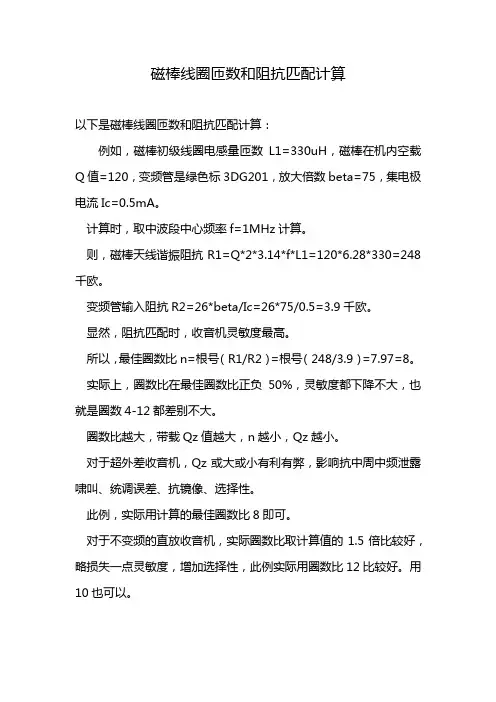
磁棒线圈匝数和阻抗匹配计算
以下是磁棒线圈匝数和阻抗匹配计算:
例如,磁棒初级线圈电感量匝数L1=330uH,磁棒在机内空载Q值=120,变频管是绿色标3DG201,放大倍数beta=75,集电极电流Ic=0.5mA。
计算时,取中波段中心频率f=1MHz计算。
则,磁棒天线谐振阻抗R1=Q*2*3.14*f*L1=120*6.28*330=248千欧。
变频管输入阻抗R2=26*beta/Ic=26*75/0.5=3.9千欧。
显然,阻抗匹配时,收音机灵敏度最高。
所以,最佳圈数比n=根号(R1/R2)=根号(248/3.9)=7.97=8。
实际上,圈数比在最佳圈数比正负50%,灵敏度都下降不大,也就是圈数4-12都差别不大。
圈数比越大,带载Qz值越大,n越小,Qz越小。
对于超外差收音机,Qz或大或小有利有弊,影响抗中周中频泄露啸叫、统调误差、抗镜像、选择性。
此例,实际用计算的最佳圈数比8即可。
对于不变频的直放收音机,实际圈数比取计算值的1.5倍比较好,略损失一点灵敏度,增加选择性,此例实际用圈数比12比较好。
用10也可以。
对于9018、9014变频管,因为放大倍数很高,最佳圈数比要重新计算。
阻抗计算之SI9000Jerry Wang概述阻抗匹配在高速电路设计中非常重要,高速电路板设计的时候通常对于关键信号都需要进行阻抗控制。
SI9000是一款很好的计算软件,之前的版本有SI6000以及SI8000,本文试图简要介绍SI9000的使用并给出SI6000和SI9000的异同。
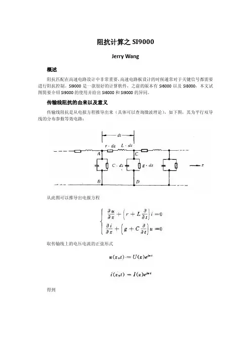
传输线阻抗的由来以及意义传输线阻抗是从电报方程推导出来(具体可以查询微波理论),如下图,其为平行双导线的分布参数等效电路:从此图可以推导出电报方程取传输线上的电压电流的正弦形式得到推出通解定义出特性阻抗无耗线下r=0,g=0则得到注意,此特性阻抗和波阻抗的概念上的差异(具体查看平面波阻抗定义)特性阻抗与波阻抗之间的关系可从LC=εμ此关系式推出。
理解特性阻抗理论上是怎么回事,再来看看实际的意义。
当电流电压在传输线传播的时候,如果特性阻抗不一致所求出来的电报方程的解不一致,就造成所谓的反射现象等等。
在信号完整性领域里,比如反射、串扰、电源平面切割等问题都可以归类为阻抗不连续问题,因为匹配的重要性在此展现出来。
叠层(Stackup)的定义下图是一种8层板常用的叠层,4层power/ground以及4层走线层,sggssggs,分别定义为L1、L2…L8,因此要计算的阻抗为L1、L4、L5和L8。
下面熟悉下在叠层里面的一些基本概念,和厂家打交道经常会使用的Oz 的概念Oz 本来是重量的单位Oz(盎司 )=28.3 g(克),在叠层里面是这么定义的,在一平方英尺的面积上铺一盎司的铜的厚度为1Oz,对应的单位如下这里需要注意的是,由于内层蚀刻表面层电镀,实际的厚度会有差别,比如内层一般的1Oz = 1.2 mil。
介电常数(DK)的概念电容器极板间有电介质存在时的电容量Cx 与同样形状和尺寸的真空电容量Co之比为介电常数:ε = Cx/Co = ε'-ε"Prepreg/Core 的概念pp 是种介质材料,由玻璃纤维和环氧树脂组成,core 其实也是pp 类型介质,只不过他两面都覆有铜箔,而pp 没有.传输线特性阻抗的计算首先,我们来看下传输线的基本类型,在计算阻抗的时候通常有如下类型: 微带线和带状线,对于他们的区分,最简单的理解是,微带线只有1 个参考地,而带状线有2个参考地,如下图所示对照上面常用的8 层主板,只有top 和bottom 走线层才是微带线类型,其他的走线层都是带状线类型。

射频阻抗匹配计算公式射频、阻抗、匹配,这几个词听起来是不是有点让人摸不着头脑?别急,让我来给您好好说道说道其中的计算公式。
咱先来说说啥是射频。
您就想象一下,射频就像是空气中快速传播的“小波浪”,比如您的手机和基站之间传递的信号,那就是射频。
而阻抗呢,您可以把它理解成电流在电路中通行的“阻力”。
这阻力大小不合适,信号传输就会出问题,就像小河流被大石头挡住,水流就不顺畅啦。
那啥叫匹配呢?匹配就是让射频信号能顺顺溜溜地传输,没有阻碍,就好比给小河流挖好了合适的河道,水就能欢快地流淌。
说到射频阻抗匹配的计算公式,常见的有史密斯圆图法、反射系数法等等。
咱先来讲讲史密斯圆图法。
这史密斯圆图就像是一张神奇的地图,您在上面能找到阻抗匹配的答案。
比如说,您知道了输入阻抗和负载阻抗,通过在这圆图上比划比划,就能算出需要添加的元件值来实现匹配。
我记得有一次,我给学生们讲这个知识点。
有个小家伙瞪着大眼睛问我:“老师,这圆图咋这么复杂呀,感觉像个迷宫。
”我笑着告诉他:“别着急,咱一步一步来,就像走迷宫找到了出口一样,会发现其实挺有趣的。
”然后我带着他们一个一个参数地分析,慢慢地,他们脸上露出了恍然大悟的表情。
再来说说反射系数法。
这反射系数就像是信号传输中的“反馈信息”,通过它能知道阻抗匹配的情况。
计算反射系数的公式看起来有点复杂,但是只要理解了其中的原理,也就不那么难了。
总之,射频阻抗匹配的计算公式虽然有点让人头疼,但只要您耐心琢磨,多做几道练习题,就一定能掌握。
就像学骑自行车,一开始可能摇摇晃晃,但多练几次,就能稳稳当当上路啦。
希望我讲的这些能让您对射频阻抗匹配的计算公式有更清楚的了解,加油!。
传输线理论,30多欧的同轴线功率容量最大,70多欧的损耗最小,取个中值50欧。
BTW,有线电视要求损耗小,一般不传大功率信号,因此75欧
用于计算特性阻抗的等式需要复杂的数学计算,通常使用场求解方法,其中包括边界元素分析在内,因此使 绝缘层的介电常数Er、走线宽度W1、W2(梯形)、走线厚度T和绝缘层厚度H。
对于W1、W2的说明:
此处的W=W1,W1=W2
规则:W1=W
W—-设计线宽
A—–Etch loss (见表)
走线上下宽度不一致的原因是:PCB板制造过程中是从上到下而腐蚀,因此腐蚀出来的线呈梯形。
走线厚度T与该层的铜厚有对应关系,具体如下
铜厚
COPPER THICKNESS
Base copper thk For inner layer For outer layer
H OZ 0.6mil 1.8mil
1 OZ 1.2MIL 2.5MIL
2 OZ 2.4MIL 3.6MIL
绿油厚度:
*因绿油厚度对阻抗影响较小,故假定为定值0.5mil。
因此使用专门的阻抗计算软件SI9000,我们所需做的就是控制特性阻抗的参数:。

阻抗匹配(zǔ kànɡ pǐ pèi)计算公式阻抗匹配(zǔ kànɡ pǐ pèi)根底(gēndǐ)知识(zhī shi)详解根本(gēnběn)概念信号传输过程中负载阻抗和信源内阻抗之间的特定配合关系。
一件器材的输出阻抗和所连接的负载阻抗之间所应满足的某种关系,以免接上负载后对器材本身的工作状态产生明显的影响。
对电子设备互连来说,例如信号源连放大器,前级连后级,只要后一级的输入阻抗大于前一级的输出阻抗5-10倍以上,就可认为阻抗匹配良好;对于放大器连接音箱来说,电子管机应选用与其输出端标称阻抗相等或接近的音箱,而晶体管放大器那么无此限制,可以接任何阻抗的音箱。
匹配条件①负载阻抗等于信源内阻抗,即它们的模与辐角分别相等,这时在负载阻抗上可以得到无失真的电压传输。
②负载阻抗等于信源内阻抗的共轭值,即它们的模相等而辐角之和为零。
这时在负载阻抗上可以得到最大功率。
这种匹配条件称为共轭匹配。
如果信源内阻抗和负载阻抗均为纯阻性,那么两种匹配条件是等同的。
阻抗匹配是指负载阻抗与鼓励源内部阻抗互相适配,得到最大功率输出的一种工作状态。
对于不同特性的电路,匹配条件是不一样的。
在纯电阻电路中,当负载电阻等于鼓励源内阻时,那么输出功率为最大,这种工作状态称为匹配,否那么称为失配。
当鼓励源内阻抗和负载阻抗含有电抗成份时,为使负载得到最大功率,负载阻抗与内阻必须满足共扼关系,即电阻成份相等,电抗成份绝对值相等而符号相反。
这种匹配条件称为共扼匹配。
阻抗匹配(Impedance matching)是微波电子学里的一局部,主要用于传输线上,来达至所有高频的微波信号皆能传至负载点的目的,不会有信号反射回来源点,从而提升能源效益。
史密夫图表上。
电容或电感与负载串联起来,即可增加或减少负载的阻抗值,在图表上的点会沿著代表实数电阻的圆圈走动。
如果把电容或电感接地,首先图表上的点会以图中心旋转180度,然后才沿电阻圈走动,再沿中心旋转180度。
阻抗匹配是指信号源或者传输线跟负载之间的一种合适的搭配方式。
阻抗匹配分为低频和高频两种情况讨论。
我们先从直流电压源驱动一个负载入手。
由于实际的电压源,总是有内阻的(请参看输出阻抗一问),我们可以把一个实际电压源,等效成一个理想的电压源跟一个电阻r串联的模型。
假设负载电阻为R,电源电动势为U,内阻为r,那么我们可以计算出流过电阻R的电流为:I=U/(R+r),可以看出,负载电阻R越小,则输出电流越大。
负载R上的电压为:Uo=IR=U/[1+(r/R)],可以看出,负载电阻R越大,则输出电压Uo越高。
再来计算一下电阻R消耗的功率为:P=I2×R=[U/(R+r)]2×R=U2×R/(R2+2×R×r+r2)=U2×R/[(R-r)2+4×R×r]=U2/{[(R-r)2/R]+4×r}对于一个给定的信号源,其内阻r是固定的,而负载电阻R则是由我们来选择的。
注意式中[(R-r)2/R],当R=r时,[(R-r)2/R]可取得最小值0,这时负载电阻R上可获得最大输出功率Pmax=U2/(4×r)。
即,当负载电阻跟信号源内阻相等时,负载可获得最大输出功率,这就是我们常说的阻抗匹配之一。
对于纯电阻电路,此结论同样适用于低频电路及高频电路。
当交流电路中含有容性或感性阻抗时,结论有所改变,就是需要信号源与负载阻抗的的实部相等,虚部互为相反数,这叫做共扼匹配。
在低频电路中,我们一般不考虑传输线的匹配问题,只考虑信号源跟负载之间的情况,因为低频信号的波长相对于传输线来说很长,传输线可以看成是“短线”,反射可以不考虑(可以这么理解:因为线短,即使反射回来,跟原信号还是一样的)。
从以上分析我们可以得出结论:如果我们需要输出电流大,则选择小的负载R;如果我们需要输出电压大,则选择大的负载R;如果我们需要输出功率最大,则选择跟信号源内阻匹配的电阻R。

换能器阻抗匹配计算1.引言1.1 概述换能器是一种将一种形式的能量转换为另一种形式的装置。
它在各种领域中被广泛应用,例如声学、电子、光学等。
换能器的基本原理是根据特定的物理原理,通过电信号或其他形式的输入驱动,将一种能量形式转化为另一种能量形式。
阻抗匹配是换能器设计中非常重要的一个方面。
换能器的阻抗匹配决定了其性能和效率。
阻抗匹配是指将发射端(或输入端)的阻抗与接收端(或输出端)的阻抗相匹配,使得信号能够最大程度地传输,减少信号的反射和损耗。
换能器的阻抗匹配需要考虑多种因素,如换能器的特性、工作频率、信号传输距离等。
一般来说,当信号源的阻抗与负载的阻抗不匹配时,会导致信号的反射和信号的损耗。
因此,为了获得最佳的信号传输效果,需要对换能器的阻抗进行合理的匹配。
本文将重点探讨换能器阻抗匹配的计算方法。
通过分析阻抗匹配的原理和依据,探讨如何计算换能器的阻抗匹配。
通过合理的阻抗匹配计算,可以获得更好的信号传输效果,提高换能器的性能。
接下来的章节将依次介绍换能器的基本原理、阻抗匹配的重要性以及本文的结论。
通过深入理解和掌握阻抗匹配的计算方法,读者可以更好地应用于实际工程设计中。
1.2 文章结构文章结构部分:本文分为引言、正文和结论三个部分。
在引言部分,首先概述了本文要讨论的主题——换能器阻抗匹配计算,并介绍了文章的结构和目的。
接下来是正文部分,主要包括两个内容:换能器的基本原理和阻抗匹配的重要性。
在换能器的基本原理中,将详细解释换能器的定义、分类和工作原理,以帮助读者对换能器有更深入的理解。
而阻抗匹配的重要性部分,则会讨论为什么在使用换能器时需要进行阻抗匹配,以及不同阻抗匹配方法的优缺点。
这两个内容将帮助读者全面了解换能器及其阻抗匹配方面的知识。
最后是结论部分,总结了本文的主要观点和结论。
结论一将指出换能器阻抗匹配的重要性和实际应用。
结论二则提出了进一步研究和改进的方向,以期为换能器阻抗匹配计算提供更精确和高效的方法。
阻抗匹配计算公式 zhihu
阻抗匹配是指将输入阻抗和输出阻抗调整为相等或接近匹配的过程。
常用的阻抗匹配图形由电感L、电容C及限流电阻R 等组成。
在电子工程中,一般使用以下公式计算阻抗匹配:
1. 并联阻抗匹配:
R = (R1 * X2 + R2 * X1) / (R1 + R2)
X = (R1 * R2) / (R1 + R2)
其中,R1和X1是输入端的电阻和电抗,R2和X2是输出端的电阻和电抗,R和X为匹配后的电阻和电抗。
2. 串联阻抗匹配:
R = R1 + R2
X = X1 + X2
其中,R1和X1是输入端的电阻和电抗,R2和X2是输出端的电阻和电抗,R和X为匹配后的电阻和电抗。
3. 电平转换阻抗匹配:
R = R1 * (Z2 - Z1) / (Z2 + Z1)
X = X1 * (Z2 - Z1) / (Z2 + Z1)
其中,Z1和Z2分别为输入端和输出端的阻抗,R和X为匹配后的电阻和电抗。
上述公式是常见的阻抗匹配计算公式,可以根据具体的情况选择合适的公式进行计算。
全差分运放阻抗匹配计算下载温馨提示:该文档是我店铺精心编制而成,希望大家下载以后,能够帮助大家解决实际的问题。
文档下载后可定制随意修改,请根据实际需要进行相应的调整和使用,谢谢!并且,本店铺为大家提供各种各样类型的实用资料,如教育随笔、日记赏析、句子摘抄、古诗大全、经典美文、话题作文、工作总结、词语解析、文案摘录、其他资料等等,如想了解不同资料格式和写法,敬请关注!Download tips: This document is carefully compiled by the editor. I hope that after you download them, they can help yousolve practical problems. The document can be customized and modified after downloading, please adjust and use it according to actual needs, thank you!In addition, our shop provides you with various types of practical materials, such as educational essays, diary appreciation, sentence excerpts, ancient poems, classic articles, topic composition, work summary, word parsing, copy excerpts,other materials and so on, want to know different data formats and writing methods, please pay attention!全差分运放是一种常用的电路元件,在电子学领域有着广泛的应用。
两层板嘉立创阻抗匹配计算在PCB设计中,阻抗匹配是一个非常重要的问题。
阻抗匹配的目的是为了确保信号在传输过程中的稳定性和可靠性。
在设计两层板时,嘉立创是一个非常常用的PCB制造商,他们提供了方便的阻抗匹配计算工具。
我们需要明确什么是阻抗匹配。
阻抗匹配是指信号源和负载之间的阻抗在一定范围内保持一致,以确保信号的传输效果。
在PCB设计中,阻抗匹配通常用于高速信号线,如DDR总线、PCIe总线等。
嘉立创提供了一个在线阻抗匹配计算工具,可以帮助设计师快速准确地计算出所需的阻抗值。
在使用该工具之前,我们需要了解一些基本的参数,如PCB板材的介电常数、板厚、铜箔厚度等。
这些参数将直接影响到阻抗的计算结果。
计算阻抗匹配的过程比较复杂,但使用嘉立创的工具可以大大简化这个过程。
首先,我们需要选择所使用的板材类型,嘉立创提供了常见的FR4板材选项。
然后,输入板材的厚度和铜箔厚度,这些参数可以在PCB设计软件中找到。
接下来,我们需要输入所需的阻抗值,一般情况下,DDR总线的阻抗要求为50欧姆,PCIe总线的阻抗要求为85欧姆。
在输入完这些参数后,嘉立创的工具会自动计算出所需的走线宽度和间距。
这些参数将作为PCB设计的输入,设计师可以直接在设计软件中使用这些参数进行布线。
嘉立创的计算结果可靠准确,可以帮助设计师避免因阻抗不匹配而导致的信号完整性问题。
除了阻抗匹配计算工具,嘉立创还提供了其他一些辅助工具,如阻抗测试板和仿真分析服务。
阻抗测试板可以用于验证设计的阻抗是否符合要求,而仿真分析服务可以帮助设计师更好地理解信号传输过程中的各种影响因素。
阻抗匹配在PCB设计中非常重要,特别是在高速信号线的设计中。
嘉立创提供了方便快捷的阻抗匹配计算工具,可以帮助设计师准确地计算出所需的阻抗值,并提供了其他辅助工具来验证和分析设计的阻抗情况。
设计师在进行PCB设计时可以考虑使用嘉立创的工具和服务,以提高设计的可靠性和稳定性。
阻抗匹配的基础解说怎样理解阻抗匹配阻抗匹配是指信号源或者传输线跟负载之间的一种合适的搭配方式。
阻抗匹配分为低频和高频两种情况讨论。
我们先从直流电压源驱动一个负载入手。
由于实际的电压源,总是有内阻的,我们可以把一个实际电压源,等效成一个理想的电压源跟一个电阻r串联的模型。
假设负载电阻为R,电源电动势为U,内阻为r,那么我们可以计算出流过电阻R的电流为:I=U/(R+r),可以看出,负载电阻R越小,则输出电流越大。
负载R上的电压为:Uo=IR=U*[1+(r/R)],可以看出,负载电阻R越大,则输出电压Uo越高。
再来计算一下电阻R消耗的功率为:P=I*I*R=[U/(R+r)]*[U/(R+r)]*R=U*U*R/(R*R+2*R*r+r*r)=U*U*R/[(R-r)*(R-r)+4*R*r]=U*U/{[(R-r)*(R-r)/R]+4*r}对于一个给定的信号源,其内阻r是固定的,而负载电阻R则是由我们来选择的。
注意式中[(R-r)*(R-r)/R],当R=r时,[(R-r)*(R-r)/R]可取得最小值0,这时负载电阻R上可获得最大输出功率Pmax=U*U/(4*r)。
即,当负载电阻跟信号源内阻相等时,负载可获得最大输出功率,这就是我们常说的阻抗匹配之一。
对于纯电阻电路,此结论同样适用于低频电路及高频电路。
当交流电路中含有容性或感性阻抗时,结论有所改变,就是需要信号源与负载阻抗的的实部相等,虚部互为相反数,这叫做共厄匹配。
在低频电路中,我们一般不考虑传输线的匹配问题,只考虑信号源跟负载之间的情况,因为低频信号的波长相对于传输线来说很长,传输线可以看成是“短线”,反射可以不考虑(可以这么理解:因为线短,即使反射回来,跟原信号还是一样的)。
从以上分析我们可以得出结论:如果我们需要输出电流大,则选择小的负载R;如果我们需要输出电压大,则选择大的负载R;如果我们需要输出功率最大,则选择跟信号源内阻匹配的电阻R。
1.阻抗的定义在具有电阻、电感和电容的电路里,对电路中的电流所起的阻碍作用叫做阻抗。
阻抗常用Z表示,是一个复数,实部称为电阻,虚部称为电抗,其中电容在电路中对交流电所起的阻碍作用称为容抗,电感在电路中对交流电所起的阻碍作用称为感抗,电容和电感在电路中对交流电引起的阻碍作用总称为电抗;阻抗的单位是欧姆。
阻抗的公式是:Z= R+j(ωL–1/(ωC))其中,负载是电阻、电感的感抗、电容的容抗三种类型的复物,复合后统称“阻抗”,写成数学公式即是:阻抗Z= R+j(ωL–1/(ωC))。
其中R为电阻,ωL为感抗,1/(ωC)为容抗。
(1)如果(ωL–1/ωC) > 0,称为“感性负载”;(2)反之,如果(ωL–1/ωC) < 0称为“容性负载”。
2.阻抗匹配阻抗匹配是指信号源或者传输线跟负载之间的一种合适的搭配方式。
匹配条件包括:①负载阻抗等于信源内阻抗,即它们的模与辐角分别相等,这时在负载阻抗上可以得到无失真的电压传输。
②负载阻抗等于信源内阻抗的共轭值,即它们的模相等而辐角之和为零。
这时在负载阻抗上可以得到最大功率。
这种匹配条件称为共轭匹配。
如果信源内阻抗和负载阻抗均为纯阻性,则两种匹配条件是等同的。
我们先从直流电压源驱动一个负载入手。
由于实际的电压源,总是有内阻的,我们可以把一个实际电压源,等效成一个理想的电压源跟一个电阻r串联的模型。
假设负载电阻为R,电源电动势为U,内阻为r,那么我们可以计算出流过电阻R的电流为:I=U/(R+r),可以看出,负载电阻R越小,则输出电流越大。
负载R上的电压为:Uo=IR=U/[1+(r/R)],可以看出,负载电阻R越大,则输出电压Uo越高。
再来计算一下电阻R消耗的功率为:P=I2×R=[U/(R+r)]2×R=U2×R/(R2+2×R×r+r2)=U2×R/[(R-r)2+4×R×r]=U2/{[(R-r)2/R]+4×r}对于一个给定的信号源,其内阻r是固定的,而负载电阻R则是由我们来选择的。
电压驻波比与阻抗匹配计算公式电压驻波比(Voltage Standing Wave Ratio,VSWR)是描述电信号在传输线上的反射程度的一个参数。
它的定义为传输线上最大电压与最小电压之比。
阻抗匹配是为了减小传输线上的反射损耗,使得信号能够更好地传输到目标设备上。
要计算电压驻波比,首先需要了解传输线的特性阻抗和负载的阻抗。
传输线的特性阻抗是指传播波的特性阻抗,常见的传输线有同轴电缆和微带线,它们都有特定的特性阻抗。
而负载的阻抗是接在传输线末端的设备的阻抗。
假设传输线的特性阻抗为Z0,传输线末端的负载阻抗为ZL,传输线上的最大电压为Vmax,最小电压为Vmin。
则电压驻波比的计算公式为:VSWR = (Vmax + Vmin) / (Vmax - Vmin)通过波的反射原理,我们知道传输线上的反射系数(Reflection Coefficient)ρ与电压驻波比存在如下关系:VSWR=(1+,ρ,)/(1-,ρ,)因此,我们可以通过计算反射系数来得到电压驻波比。
对于传输线上的反射系数,它与传输线特性阻抗和负载阻抗之间有一个关系。
当传输线特性阻抗和负载阻抗相等时,反射系数为0,此时电压驻波比为1,表示完全匹配。
而当传输线特性阻抗和负载阻抗差异较大时,反射系数会增大,电压驻波比也会增大,表示不完全匹配。
为了实现阻抗匹配,我们可以采取一些措施。
例如,在传输线末端引入匹配网络,通过调节匹配网络的参数来使得传输线特性阻抗和负载阻抗相等。
匹配网络可以采用传输线、衰减器、变压器等组件来实现。
另外,在设计传输线时,也可以采用特定的传输线结构和材料,使得传输线特性阻抗和负载阻抗接近。
阻抗匹配的目的是为了最大限度地减小反射损耗,提高信号传输效率。
当传输线上的反射系数接近零时,表示反射损耗很小,信号能够更好地传输到目标设备上。
反之,当反射系数较大时,反射损耗就会增大,信号传输效果不佳。
总结一下,电压驻波比是描述电信号在传输线上反射程度的参数,其计算公式为VSWR = (Vmax + Vmin) / (Vmax - Vmin)。
polar An Introduction to the Design andManufacture of Controlled Impedance PCBsControlled Impedance PCBsWe produced the first edition of this booklet several years ago in response tomany requests for a basic introduction to the manufacture of controlledimpedance printed circuit boards (PCBs). In this second issue, we have addedextra material to some sections and introduced a number of new topics to reflect the changes that have occurred in the industry over the last few years. We have tried to explain the most important concepts and address the most frequentlyasked questions with the minimum of technical jargon.You can download this document as a pdf file from www. or alternatively, ask your local distributor or Polar Instruments if you requirefurther copies.We hope that you find it useful and welcome any comments you may have e.g.areas where you would like more detail, suggestions for new topics, etc. Please email your comments to us at mail@.IndexPage234457891112131415161718The cable that connects the antenna to the television is a common example of a controlled impedance that most of us are familiar with.This cable may be one of two types:A coaxial cable consists of a round, inner conductor, separated from the outer cylindrical conductor (the shield) by an insulator. The dimensions of the conductors and insulator, and the electrical characteristics of the insulator are carefully controlled in order to determine the shape, strength and interaction of the electrical fields which, in turn, determine the electrical impedance of the cable.Instead of a coaxial cable, an antenna may be connected to the set by means of a cable formed of two round wires spaced by a flat strip of plastic. As with the coaxial cable, the dimensions and materials of this wire are carefully controlled so as to give it the correct electrical impedance.These two cables are examples of different configurations of a controlled impedance but there are many others. In the same way, you will learn that there are many different trace configurations that are used in the PCB industry to achieve a controlled impedance. Controlled impedance PCBs emulate controlled impedance cables, where the coax shield may be represented by a plane, the insulator represented by the laminate, and the conductor is the trace. Just as for the cables, the impedance is determined by the dimensions and materials, and these parameters must be very carefully predicted in design, and then controlled in the manufacturing process to ensure that specifications are met.Impedance is measured in Ohms (symbol Ω) but is not to be confused with resistance, also measured in Ohms (also with symbol Ω). Resistance is a DC characteristic, whilst impedance is an AC characteristic which becomes important as the signal frequency increases, typically becoming critical for PCB traces at signal components of two or three hundred MHz and above.What is controlled impedance?23Impedances MatchedImpedances MismatchedThe function of a wire or trace is to transfer signal power from one device to another.Theory shows that maximum signal power is transferred when impedances are matched. A TV antenna has a "natural" characteristic impedance. At RF frequencies of between hundreds of MHz (megahertz) and GHz (gigahertz), the transfer of maximum signal power from the antenna to the cable requires that the cable impedance match the antenna impedance. Also, the TV impedance must match the cable impedance. Hence, there is a matched system where the antenna to cable to TV impedances all closely match and themaximum amount of signal is transferred from the antenna to the cable and thence to the TV .Where there is an impedance mismatch,maximum signal power transfer does not occur.Only a portion of the signal power istransferred from the sending device into the receiving device (coax, PCB trace, etc.) The remainder of the signal power is reflected back to the sending device.Suppose a cable of incorrect impedance links the antenna to the TV . Thus, the TV antenna and the cable impedance do not match, and not all of the TV signal detected by the antenna will pass from the antenna into the cable. Some will be reflected back into the antenna and be re-radiated. Thus the TV will not receive the maximum signal available, and picture quality may deteriorate.Next, since the cable impedance does not match the TV impedance, not all of the signal conveyed by the cable will pass into the TV .Why do we need controlled impedances?Although we have focused on wire interconnections, exactly the same considerations apply to signal transfer through traces on a PCB. When board traces carry signals containing high frequencies, care must be taken to design traces that match the impedance of the driver and receiver devices. The longer the trace, or the greater the frequencies involved, then the greater the need to control the trace impedance. The PCB manufacturer controls the impedance by varying the dimensions and spacing of the particular trace or laminate.Any impedance mismatch can be extremely difficult to analyse once a PCB is loaded with components. Components have a range of tolerances, so that one batch of components may tolerate an impedance mismatch, while another batch might not. Moreover, a component’s characteristics may change with temperature, so that the problems may come and go. Thus, if changing a component appears to cure a problem, the components may become the suspects instead of the trace. Component selection becomes the solution, and build costs are driven up, while all the time the real fault – trace impedance mismatch – goes undetected!For these reasons, a PCB designer will specify trace impedance and tolerance, and should work with the PCB manufacturer to ensure that the PCB meets the specifications.As recently as 1997, only exotic, high-speeddevices of the time required controlledimpedance PCBs. These amounted to perhaps20% of PCBs manufactured. In 2000, around80% of all multilayer PCBs are manufacturedwith controlled impedance traces. These wouldinclude boards for all types of technologiesincluding* telecommunications (analog or digital)* video signal processing* high speed digital processing* real time graphic processing* process controlMost homes today have numerous low-cost applications of these technologies, for example* Modems, cordless phones, personal radiocommunicators, analog or digital TV,satellite TV, GPS, radar.* Video games, digital cameras and digitalvideo cameras, DVDs.* Low cost personal computers, CDs, colour printers* Digital TVs, DVDs, Instant Playback TVs* Auto engine control modules.Industry and commerce are awash with thesesame technologies, and the lists are continually expanding. We can therefore expect that in thenear future virtually all PCBs will include atleast some controlled impedance traces.Controlled impedance has become the norm.Types of systems that use controlled impedance PCBs.Controlled impedances on PCB traces4Embedded Microstrip contains a tracesandwiched within the PCB with a plane on one side and laminate and then air on the other.Offset Stripline contains a trace sandwiched within the PCB with a plane on both sides of the laminate.Edge coupled coated microstrip is a differential configuration where there are two controlled impedance traces on the surface, coated by resist and a plane on the other side of the laminate.Edge coupled offset Stripline is a differential configuration with two controlled impedance traces sandwiched between two planes. The traces are shown offset, however they could be midway between the planes (2H1+T=H).These diagrams are examples of some of the many different configurations that PCB designers can use. When you are looking at the stack up of a multiplayer PCB, remember that controlled impedances are shielded by planes and for this reason, you only need consider the laminate thicknesses between the planes on either side of the trace when it is inside the PCB.5This differential configuration has two traces thatare separated by laminate and sandwichedbetween two planes. Although the diagramshows the traces offset, the manufacturingobjective is to have the traces with no offset, i.e.one should be directly above the other. Typically,this configuration is difficult to fabricate.In this Coated Coplanar Strips configuration,there is a single controlled impedance tracewith two ground traces of a specified width(W2/W3) either side. All the traces are coatedwith resist.The Coplanar Waveguide has a singlecontrolled impedance trace with planes eitherside (or very wide ground traces), a continuousplane on one side and laminate only on theother side.This Coplanar Waveguide is similar to theabove configuration except that there areplanes on both sides of the laminate as well asa plane on the same layer as the controlledimpedance trace.6Manufacturing Controlled Impedance PCBs.As the operating speed of electronic circuits has increased, so has the need for PCBs to have controlled impedances and the majority of PCB manufacturers are producing them. As described earlier, if the value of controlled impedance is incorrect, it can be very difficult to identify the problem once the PCB is assembled. Since the impedance depends on many parameters (trace width, trace thickness, laminate thickness, etc.) the majority of PCBs are currently 100% tested for controlled impedance. However the testing is not normally performed on the actual PCB but on a test coupon manufactured at the same time and on the same panel as the PCB. Sometimes the test coupon is integrated into the main PCBSometimes your PCB customer is not aware that testing is best accomplishedusing test coupons and you, as the PCB manufacturer, will need to explainthe benefits of coupons which include:* It is rare for controlled impedance traces tobe easily accessible for testing (including aclosely situated ground connection).* Planes are not interconnected on the mainPCB and this may lead to inaccuratemeasurements.* Accurate and consistent testing resultsrequire a straight single trace of 150mm (orlonger), often the actual PCB trace is shorterthan 150mm.* The actual PCB trace may have branches orvias which makes accurate measurement verydifficult* Adding extra pads and vias for testing onthe PCB will affect the performance of thecontrolled impedance trace and will occupyspace needed for the function of the PCB.The typical test coupon is a PCB approximately 200x30mm with exactly the same layer and trace construction as the main PCB. It has traces which are designed to be the same width and on the same layer as the controlled impedance traces on the main PCB.When the artwork is produced, the sameaperture code (D-code) used for the controlled impedance traces is used to produce the test traces on the coupon. Since the coupon is fabricated at the same time as the main PCB the coupon’s traces will have the same impedance as those on the main PCB. All planes are included on the coupon and they are interconnected on the coupon only, to ensure that test results are valid. It is necessary to include a void around the coupon on the reference planes so as not to affect the connectivity of the PCB itself if BBT(Bare Board Test) occurs whilst still on the panel.Usually one coupon is made at the end of each panel to ensure that the coupon is representative of the whole panel i.e. testing the 2 coupons will verify to a high confidence level that there are no differences in trace width, trace thickness, laminate height, etc. over the whole panel.In fact some customers use the measurement of controlled impedance traces on test coupons on each panel to check the overall quality of PCB manufacture even when the PCB contains no controlled impedances. Since the coupon’s controlled impedance depends on all the PCB parameters, it is a very accurate measure of consistency of manufacture without sectioning the PCB.In addition to the usual PCB specifications, thePCB designer should specify:* Which layers contain controlledimpedance traces* The impedance(s) of the trace(s) (there canbe more than one value of impedancetrace per layer)* Separate aperture codes for controlledimpedance traces e.g. 4 mil non controlledimpedance trace and 4 mil controlledimpedance trace.* And either:1. the width (w) of the controlledimpedance traceor2. the laminate thickness (h) adjacentto the controlled impedance traceIn case 1, where trace width (w) is specified,the manufacturer will adjust the laminate thick-ness (h) to give the correct value of impedance.In case 2 where the laminate thickness (h) isspecified, the manufacturer will adjust the tracewidth (w) to achieve the value of impedance.Some configurations (differential, coplanar)may have more than one parameter that can bevaried to obtain the specified impedance.8Exploded view of a test couponExploded view ofa test coupon 9Solder maskL1 Coated MicrostripPre PregL2 Reference (ground) plane LaminateL3 Differential Stripline Pre PregL4 StriplineLaminateL5 StriplinePre PregL6 Differential StriplineLaminateL7 Reference (ground) planePre PregL8 Coated microstrip Solder mask10Typical Test CouponNote that you can download Gerber files for a typical impedance test coupon from .Typical Test Coupon(Reference IEC draft, addition to IEC326-3)1Dielectric separation will replicate impedance structure on printed boards.2.Test connection holes shall be plated through to access all inner layer test conductors.3.Square pads identify plated through holeconnections to access all ground/power reference planes.4.Conductor widths will replicate critical conductors on each impedance layer.5.Via holes to be added as required.6.Cross hatching to be added to outer layer as required.7.Two coupons per panel. These to be individually identified with letter A & B respectively.8.Job No. + Datecode to be added as per customer requirements.9.All planes to be interconnected (on test coupon only).Capacitive loadingTo minimise capacitive loading during test, you should minimise the size of pads and vias on coupons, especially for high impedance traces. Although this standard coupon design shows pads at both ends, you are likely to obtain better test results on high impedance traces if you only place a pad at one end.L1L3L5L7183.49203.2172.70170.16167.629.8615.8813.3510.8031.7512.80not to scale 5.08 2.545.082.54Calculating the value of impedances using Field Solvers11A few years ago, you could use simple published equations to obtain the nominal values of trace dimensions for a particular impedance and they were reasonably effective for line widths and spacing above 15 mil (thousandths of an inch). However these simple equations are only approximations and do not give accurate results for line widths used on current technology PCBs.You will need to use Field Solver softwarefor calculation of controlled impedances.Their effectiveness is enhanced ifthey offer "goal seeking" that letsyou enter the desired impedance andthe field solver calculates the trace dimensions.Polar Instruments pro-duces Field Solver softwarespecifically forthe prediction of PCB trace impedances based on trace configuration, trace geometry and material characteristics. You can download free, functioning demonstration versions of the software from our website at12Measuring controlled impedances It is also useful to microsection some of the coupons to verify the actual dimensions of the traces compared to the nominal values. These measured dimensions can be used in theequations to calculate an impedance value from the actual dimensions, adding a third column to your table of results.We should mention that the presence of solder resist affects the impedance of surfacemicrostrip and you should include this in your characterisation process.Impedances typically range between 40 ohms to 120 ohms. The higher impedances are more difficult to control since they typically have narrower traces and will be relatively more affected by the exact etch process (i.e. since the impedance is inversely proportional to the trace width and thickness, as traces become very thin, the relative effect of the etching process will have a greater effect on their width and profile and hence, impedance).The following relationships will give you an idea of how impedance depends on dimensions,however please remember they are only approximations for fine line widths:• Impedance is inversely proportional to trace width• Impedance is inversely proportional to trace thickness• Impedance is proportional to laminate height • Impedance is inversely proportional to the square root of laminate ErUsing Field Solver software is a good startingpoint for obtaining nominal values of trace width (w) and laminate thickness (h) to obtain specific values of impedance. However you will need to produce test panels containing many coupon designs, with different trace widths, different configurations (Stripline,Microstrip, Embedded Microstrip) and different layer structures with different laminate /pre-preg thicknesses.Ideally you will produce standard coupons (see suggested design) and each coupon can contain a variety of different impedances. After manufacture of the test panels, you will then need to measure the actual values of impedance and see how they correlate against theoretical values.Laminate suppliers will provide you with lists of Er (dielectric constant) for different core constructions, typically FR-4 has Er=4.2. If you use preferred core material, you will be assured of consistent performance characteristics. By constructing a table of results comparing the measured values with the calculated values,you will see the variance between your process and the theoretical calculations. You can then remake the test panels, altering (w) and / or (h)to obtain the "exact" design values of imped-ance. After several iterations, you will have an understanding of your process that allows you in most cases to take the designers’requirements and convert them into values that suit your process and produce boards whose impedances are centred around the specified nominal impedance to maximise yield.Characterising your manufacturing process13Impedances can be measured using:• A Network Analyser• A laboratory Time Domain Reflectometer (TDR)• A Controlled Impedance Test System (employing TDR techniques)Both Network Analysers and laboratory TDRs are highly complex and sophisticated laboratory instruments that typically need to be operated with great care even by a skilled engineer. A Controlled Impedance Test System (employing TDRmeasurement techniques) that is specifically designed for measuring controlled impedances on PCBs offers the optimum solution.A TDR applies a very fast electrical step signal to the coupon via a controlledimpedance cable (and preferably a matching impedance probe). Whenever there is a change in impedance value (discontinuity), part of the signal power is reflected back (as discussed earlier) to the TDR instrument which is capable of measuring this reflected signal.The time delay between the transmitted pulse and the receipt of the reflected signal is proportional to the distance of the discontinuity. The magnitude of the reflected signal is related to the value of the discontinuity.From this data it is possible to graph impedance versus its position on the testcoupon. This is typically achieved using software to control the TDR and to acquire and process the data which it produces.A TDR specifically appropriate for the measurement of PCB controlled impedance in a manufacturing plant should be able to:• Be operated reliably and conveniently in the normal plant environment by a non-technical person with minimum training requirement.• Offer a degree of test automation for high throughput lines.• Produce easy-to-understand results in the form of graphs of impedance versus distance over the length of the test coupon.• Indicate and log unequivocal Pass/Fail results for each device tested.• Datalog results and produce reports suitable for presentation to the customer.• Store test files which contain the specifications for each type of coupon produced, and automatically set up the TDR.Measuring controlled impedancesPolar Instruments designs and manufactures rugged, manual and robotic Controlled Impedance Test Systems specifically for PCB measurements in themanufacturing environment.Polar is a world leader supplying instruments to premier PCB manufacturers around the globe.Using airline standardsPrecision airlines are accepted as the"standard" for controlled impedances.They consist of two accurately machinedconcentric tubes where all of the dimensionsare very tightly controlled, terminated with asuitable connector. TDRs used for impedancemeasurement are precision measurementinstruments and need to be regularly calibrated.Reference air line standards are used for TDRcalibration and are available in a variety ofstandard impedances (typically 28Ω, 50Ω, 75Ωand 100Ω).Precision air lines are a high cost item and anacceptable alternative for less criticalapplications is a set of precision semi rigidcables calibrated against air lines.Air lines are made traceable to NationalStandards (NIST, NPL) by a precisionmetrology technique called air gauging whichallows the bores of the air line to be measuredand the impedance calculated using a standardformula.14Many modern designs use a differential pair of traces between components. When compared to a single trace, differential configurations are less susceptible to interference from adjacent traces and generate less interference.To be effective, they need to be matched i.e.:• Both traces should have the same dimensions and spacing to adjacent traces and planes • The traces should be as close as possible to each other as the manufacturing process allows• The spacing between the two traces should be constantThe value of the controlled impedance depends on the trace separation as well as the dimensions of the individual traces and when you are measuring them, you will need to make a differential measurement.Typically the differential measurement will be slightly below twice the value of the impedance of each trace e.g. if you measure each individual trace of a 100Ωdifferential pair,they are both likely to read around 53Ωor 55Ω.Coplanar configurations have becomeincreasingly popular in the past few years andare widely used for Rambus TM. One of thebenefits of surface coplanar configurations isthat they extend the operating frequency ofFR4 laminate which loses performance above2Ghz. In surface coplanar, most of the fieldbetween the trace and plane is through airrather than the laminate and so the loss causedby the laminate has less effect at highfrequencies.There are many variants of coplanar con-figurations and you should also be aware thatcoplanar differential traces can be fabricated.This diagramshows just oneof the manycoplanarconfigurations .15Q A16Typical Questions and AnswersQ. My customer says I need to test their PCBs at 900MHz. Can I do thiswith a TDR based test system?A. Yes, a TDR based impedance test system is suitable for testing over awide range of frequencies. The parameters that determine impedance (laminate Er) do not vary significantly below 3 to 4GHz. So it isunnecessarily expensive and time consuming to do a single frequency test using a network analyser.Q. My customer does not specify that I measure controlled impedances,what should I do?A. Your customer may think that by specifying the dimensions, the traceswill automatically have the correct value of impedance. As explained earlier,each manufacturing process requires characterisation to ensure that the process is matched to nominal values produced by Field Solver calculators.Your customer will not be satisfied if their PCBs fail because the final value of controlled impedances are incorrect. Work in partnership with your customer and help them understand the need for test.Q. How do I calculate the dimensions for controlled impedances on innerlayers on my stack up?A. You can ignore any layers that are beyond the planes either side of thetrace being calculated. You only need to consider the laminate thicknesses either side of the trace to the nearest planes on both sides. You can think of this as the plane forming a shield either side of the trace.Q. Why are all of the impedances measurements on my coupon are wrongbut the dimensions agree with the Field Solver?A. You have probably forgotten to connect all of the planes to each other.This is necessary to obtain the correct values. Remember that this should be done on the coupon only and you should leave a void around the coupon to avoid these interconnections affecting bare board test if the coupon is attached.You canread and download a wide range of Application Notes from our website atw w w.p o l a r i n s t r u m e n t s.c o m.The Polar Instruments CITS controlled impedance test system has become the industry standard for use by non technical operators in manufacturing environments.It is also widely used by CEMs to verify conformance of incoming PCBs.CITS uses TDR techniques tomeasure controlledimpedances and itautomatically reports when ameasurement is outside thespecified tolerance. Itautomatically processes thedata to produce a simpledisplay of impedance versusdistance.All results and system set up data areautomatically datalogged. Data can be easilyexported to a third party database (eg forstatistical process control). Test Reports canbe produced suitable for supply to customers.High accuracy is assured with instruments thatrun 32 bit software as they are factorycalibrated against precision reference airlines at28, 50, 75 and 100 ohms, all traceable toNational Standards. Users report excellent gageR&R results.17The Polar Instruments RITS robotic impedance test system is used for medium to high volume testing of controlled impedance PCBs. The measurement system is based on the industry standard CITS with robotic automation speeding the throughput and offering unparalleled accuracy, reliability and consistency of test.Controlled Impedance Test Systems (CITS)Robotic Impedance Test System (RITS)Impedance calculation using SI6000 Field SolversSI6000 is the result offeedback from the hundredsof customers who use PolarCITS25 for controlledimpedance design. New FieldSolvers in the SI6000A allowyou to graph impedanceagainst various PCBparameters.Using Excel 97 or 2000 as apowerful and convenient userinterface, the SI6000A can beused as supplied to goal seek for variousdesigns or graph Zo against a range ofparameters.The SI6000A supports a huge number ofpopular impedance controlled structures andallows you to fully evaluate their behaviour.You benefit by producing impedance controlledboards with better yields and as a result havefewer board turns before ramping upproduction.You can download an evaluation copy fromour website18。