
ATE solutions to 3D-IC test challenges The rea diness of Advantest’s V93000
Scott Chesnut scott.chesnut@https://www.doczj.com/doc/1f9618889.html,
Robert Smith robert.j.smith@https://www.doczj.com/doc/1f9618889.html,
Florent Cros florent.cros@https://www.doczj.com/doc/1f9618889.html,
Lakshmikanth Namburi lakshmikanth.namburi@https://www.doczj.com/doc/1f9618889.html,
Advantest America
San Jose, California USA
Abstract—Three dimensional integrated circuits (3D-IC) require that automatic test equipment develop capability to address the challenges brought on by these structures.
Such capability is found in test solutions which provide multiple clock domains, granular hardware porting per 3DIC layer, powerful test languages to control this hardware and collaborative software development environments.
Advantest’s introduction of clock domain per pin, multi-port, concurrent test, and protocol aware software, MEMS probes, and SmarTest program manager address the test challenges of 3DIC in an effective effectively. They allow production solutions to be architected to the degree of granularity required by the development teams.
Keywords—Protocol aware, Clock domain per pin, multi-port hardware, concurrent test framework, Protocol aware, SmarTest program manager, PLL Keep Alive, 3DIC TSV, 25uM pitch, MEMS Probes, ATE, BIST, JTAG, Pico Ampere Meter, interposer, spatial translation, MEMS, planarity, probes, cantilever, beam.
I.I NTRODUCTION
3D chips are multi-system entities whose test challenges dwarf those presented by yesterday’s System in a Package (SiP) and/or System On a Chip (SOC). Substantial infrastructure must be readied in order to position any Automatic Test Equipment (ATE) to succeed in a production test environment. A good approach to understanding what the real challenges are would be to eliminate those with already known solutions.
Past efforts to reduce test time, increase test coverage, and coordinate the software efforts of large groups of test engineers have solved 2D related production test problems. While these solutions had been developed for reasons other than 3DIC/TSV production test, we find they may lend themselves well to the task. Many of the perceived 3DIC/TSV test problems actually already have solutions. What follows is a description of how the existing features of Advantest’s V93000 might address many of these challenges.
A.Test Program Software Maintenance – SmarTest Program
Manager.
Historically, a chip had one function. As more functions where added they became systems on a chip and then the migration to system in a package occurred. 3DIC systems in a stack add even greater complexity.
Whether 3D stacks are assembled from Known Good Die (KGD) or Pretty Good Die (PGD) it can be assumed that “some” level of test will occur at both the chip level and then the stack level. Without assurance that chip layers are somewhat functional, a single layer’s defect can result with failing of the entire stack. Test costs become prohibitive as many good die are lost due to a single bad layer.
Testing die before and after stack assembly requires use of variations of the same test program. One program version is used for the single die, another for the assembled stack. This is because test at the chip level will target its subcomponents while test at the stack level will exercise mission mode system level performance.
It is likely that the same program be used for both activities with the difference being in how it perceives its current purpose. That is, a well architected test program can receive instructions from an operator or prober/handler and branch into chip or stack level test.
Whether testing PGD, KGD, on the chip or stack level, use of the same program to test both reduces the correlation burden between chip test and assembled stack test. Proper maintenance of these program variations will require tighter book keeping than in the past.
3D structures, being built from multiple separate chip layers have associated with them legions of test, product and design engineers responsible for performance of each layer. Large groups of people who, while in the past never had reason to collaborate, in the future will find it absolutely necessary. Since each layer represents man years of test development effort, the test programs of each engineering group will have
to be integrated into a single large master test program whose purpose is test the entire stack or portions of it as it is built.
Collaborative test development software packages must enable graceful checking in and out of test program modules with a minimum of inter-group interaction and/or miscommunication. Ideally, it would also address multi-platform customer concerns because the intellectual property of a given test is expected to come from bench data, EDA tools, Verilog simulations and/or competing testers.
A method of handling this task is found in Advantest’s SmarTest Program Manager. While the product has many features which ease program generation, version control, translation, and test time reduction, it also allows effective collaboration between any number of engineers who independently debug, modify, and re-integrate changes into the master test flow. Already a highly mature product SmarTest Program Manager lends itself well to the task of 3DIC test software development, integration and maintenance.
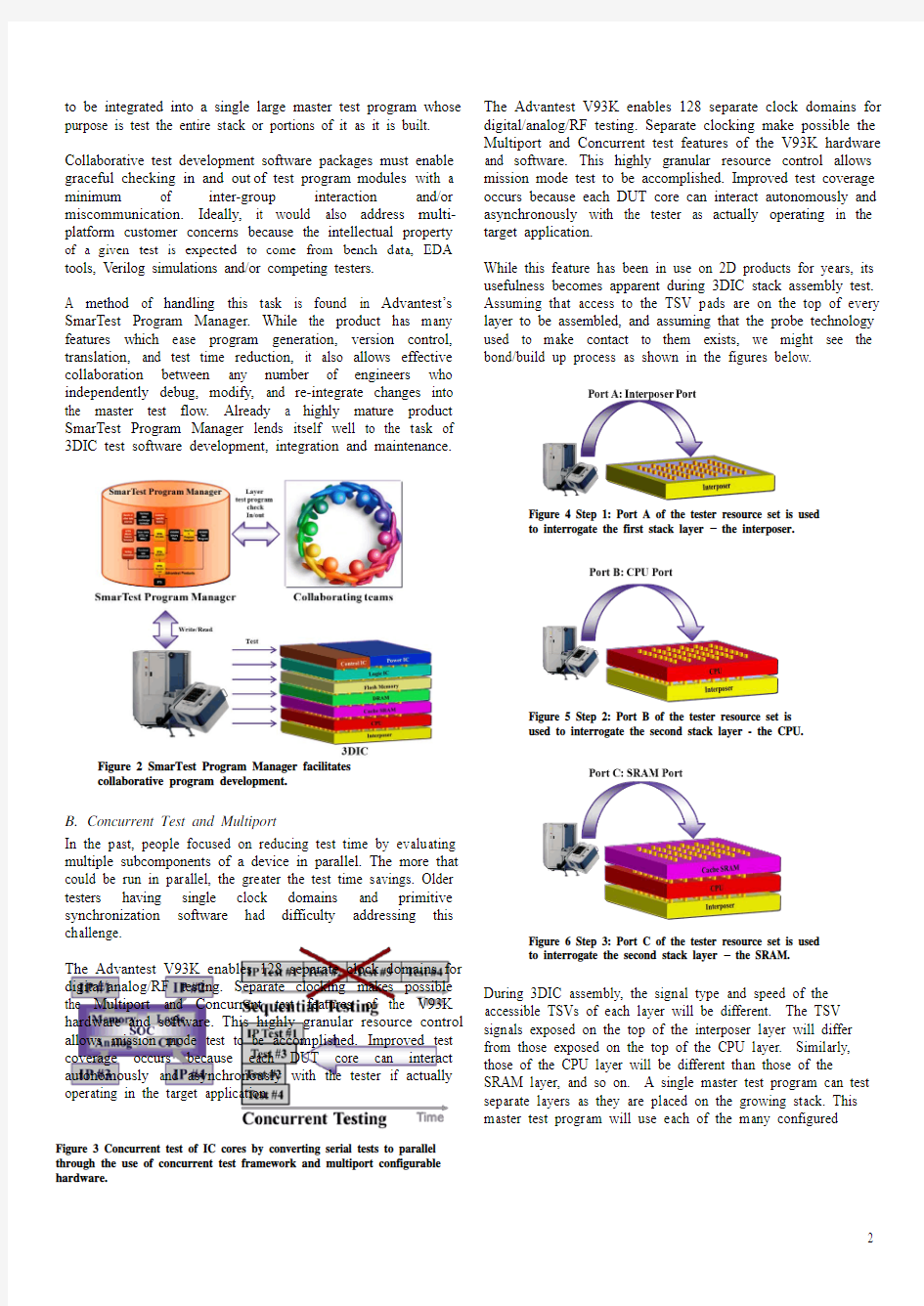
B. Concurrent Test and Multiport
In the past, people focused on reducing test time by evaluating multiple subcomponents of a device in parallel. The more that could be run in parallel, the greater the test time savings. Older testers having single clock domains and primitive synchronization software had difficulty addressing this challenge.
The Advantest V93K enables 128 separate clock domains for digital/analog/RF testing. Separate clocking makes possible the Multiport and Concurrent test features of the V93K hardware and software. This highly granular resource control allows mission mode test to be accomplished. Improved test coverage occurs because each DUT core can interact autonomously and asynchronously with the tester if actually operating in the target application.
The Advantest V93K enables 128 separate clock domains for digital/analog/RF testing. Separate clocking make possible the Multiport and Concurrent test features of the V93K hardware and software. This highly granular resource control allows mission mode test to be accomplished. Improved test coverage occurs because each DUT core can interact autonomously and asynchronously with the tester as actually operating in the target application.
While this feature has been in use on 2D products for years, its usefulness becomes apparent during 3DIC stack assembly test. Assuming that access to the TSV pads are on the top of every layer to be assembled, and assuming that the probe technology used to make contact to them exists, we might see the bond/build up process as shown in the figures below.
During 3DIC assembly, the signal type and speed of the accessible TSVs of each layer will be different. The TSV signals exposed on the top of the interposer layer will differ from those exposed on the top of the CPU layer. Similarly, those of the CPU layer will be different than those of the
SRAM layer, and so on. A single master test program can test separate layers as they are placed on the growing stack. This master test program will use each of the many configured
Figure 2 SmarTest Program Manager facilitates
collaborative program development.
Figure 3 Concurrent test of IC cores by converting serial tests to parallel through the use of concurrent test framework and multiport configurable hardware.
Figure 4 Step 1: Port A of the tester resource set is used
to interrogate the first stack layer – the interposer.
Figure 5 Step 2: Port B of the tester resource set is used to interrogate the second stack layer - the CPU. Figure 6 Step 3: Port C of the tester resource set is used to interrogate the second stack layer – the SRAM.
ports, each architected to serve the needs of every layer. In this way as layers are bonded on the stack and as the profile of the accessible signal sets change, a new test program need not be loaded into the tester. Multiple separate programs will not be needed.
C. Clock Domain per Pin
Advantest’s Multiport allows the hardware assignment granularity required to test discrete 3DIC layers and cores within each layer. As mentioned previously, another such feature is clock domain per pin capability of Advantest’s
PS1600 and PS9G digital pins. Such functionality allows each layer or layer sub function to operate in any of up to 128 total asynchronous clock domains, each supporting independent periods resolved to 3nS. This can be considered a requirement for future 3DIC designs because the integration of multiple IP cores on stack layers will require multiple clock
frequencies/domains. Mission mode setup and operation becomes an issue as more layers of the stack are assembled because direct access to sunken layers will become obscured. The only way to operate the partial stack will be if the ATE can achieve this functionality. Hence ATE targeting 3DIC test needs to be a flexible multi clock domain instrument as well as one supporting Multiport.
As seen in Fig. 7, the Advantest test equipment can be configured to operate each individual layer at its required asynchronous clock rate. Stack layer clock rates will have to be provided whose frequencies are dissimilar to the point of only being fractionally related to those around them. Multiple free running clocks will have to be provided to different layers again at different rates. PCI express, PXI, SLIM bus, etc. protocols will be expected to run simultaneously on different parts of digital hardware while unrelated RF/mixed signal activities occur autonomously as well. Data bus rates of multiple layers can be expected to have unique timing requirements unto themselves.
D. Protocol Engine per Pin
As the 3D chip is built and tested, bottom layers will have been designed to communicate with others which are not yet present. Again, this type of communication is expected to be done in mission mode. A tester will have to become the
“surrogate stack” until future layers are assembled. It will be required that the ATE act to perform the virtual functions of the remaining un-built stack layers in order to facilitate the mission mode testing of the targeted layer as well as the layers underneath it. It becomes necessary to use protocol aware to make the stack “think” it is talking with the rest of itself even though it’s yet not there. A tester implementing protocol
aware allows the tester to act as the remaining un-built portion of the stack.
But physical challenges occur as the stack layers are built up. These stem from the fact that the X-Y locations of a given signal set will change from layer to layer. That is, pads whose purpose was to send/receive PCIE signals at topological location A on layer 1 may be found at location F on layer 2. This is generally known as the “spatial translation” of a given signal set from layer to layer.
To compound the problem, on layer 2 the pads at location A may be required to perform I2C protocol not PCIE. Normally, to accommodate this would require a separate probe
arrangement for each layer meaning a separate probe card for each layer and a separate way of handling the protocol change. Alternatively, since the V93000 port granularity allows for
Figure 8 As stack layers are added, the tester must mimic the function of future, not yet present layers
Early in the assembly/test process
Later in the assembly/test process
reassignment of digital pins from one port to another in a dynamic fashion, this exception is handled. Probe card pins which test I2C on one layer can be reconfigured as PCIE on another. This is because the V93000 supports the Protocol Engine per pin which means the same pin can test either
protocols (or any other for that matter) on the same probe pin (same X-Y layer location) across all of the layers.
Unfortunately, if the type of spatial translation is occurring between layers and moves from digital to RF or mixed signals, this solution falls apart because the function of the tester
resource changes entirely thus requiring reassignment of probe card wiring to a different tester resource or a local relay implementation. Possible solutions to this problem are:
1. Develop a JEDEC (Joint Electronic Device
Engineering Council) standard which enforces strict TSV signal type assignment rules. But this will require all layer vendors to observe defined
conventions. As of the date of this writing, JEDEC has yet to develop a complete standard.
2. Design every tester pin to accommodate every signal
type: RF/Power/Mixed Signal/Digital. This is an impractical, expensive, and multi-man year solution to develop.
3. Re-route probe cards for every layer. This requires
multiple separate probe cards - one for every layer which would be expensive.
4. Use interposers to perform the spatial translation.
While this adds to the assembly burden, it is a
flexible solution which could handle physical layout exceptions. But as such requires that all interposers be individually tested.
The most practical currently available solution to this problem would be to introduce interposers between layers to route signals of a given type to a region of the probe card where
these tester resources have already been assigned. In this way, repositioning of the probe arrangement by way of another probe card is not required (eliminating the requirement for multiple probe cards and the time to change them).
E. Interposers
There has been recent focus on the use of interposers to
perform the intra-layer spatial translation. This is so not only for the reasons specified above (to avoid spatial translation of digital to RF signals and to address mechanical pitch
mismatches) but also because use of them relinquishes chip designers from the responsibility of routing signals to the TSV x/y locations required by the next/previous layers of the stack. While the JEDEC consortium outlines the standard JESD49A, which suggest conventions where by these designer might compromise their efforts it is not complete; a simpler solution
may the use of interposers.
The word “interposer” comes from the Latin, interpōnere,
meaning 'to put up between'. In the context of 3DIC test an interposer will perform the spatial translation of signals coming from one layer’s X/Y positions to that of the next layer. The interposer will be “put in between” layers in order to route signals using conductive paths.
Interposers can be used to route signals of a given nature to
probe card pins which are already assigned to that type of
Figure 12 Simplified Interposer Concepts. Signals from bottom side
being routed to a different location on the top. Same side signals
being routed to different locations.
Figure 9 PCIe port being tested on layer 1 at locations A.
Figure 10 Locations A on layer 3 is tested as a memory interface. Location F now tests the same PCIe pins as on layer 1 now spatially translated from locations A on layer 4.
Figure 11 Locations A tests I2C protocol.
Location F interfaces with Power
Management and is concurrently tested at an
asynchronous rate using a different
communications protocol.
X-Y Locations ―A‖ test function
from PCIe to Memory
tester resource signal (RF/mixed signal/digital/power). This eliminates the requirement to swap probe cards during intra-layer production test of the stack.
The number of TSVs found in future 3D devices is expected to be large - hundreds or thousands on top and bottom of each layer. The conductive traces on interposers will be comprised of very small geometries and tax the limits of mechanical fabrication tolerances. Because of this, a great number of the traces (if not all) are to be tested if for no other reason than to check process variations.
To test interposer trace connectivity in production will require more than just continuity. The current carrying capability of each trace is expected to be very low – too low for standard ATE parametric instrumentation to be able to resolve. While Time Domain Reflectometry (TDR) techniques can be used to validate/characterize line length, continuity, and possibly impedance, it cannot verify current carrying capability
(conductance). The Advantest Pico-amp Measure Card, can do all of these. Line length is verified by resistivity per cubic millimeter and knowledge of ideal trace volumetric and or cross sectional dimensions.
It is a requirement that interposer test be as thorough as that found in Known Good Die. By the time an interposer is to be attached to the stack it must be 100% functional. It will make sense to bond the interposer on the die layer without testing the TSV it lays on. All that will need to be evaluated will be the bonding process. This occurs during the normal course of that layer’s mission mode test.
The described approach solves the spatial translation problem associated with digital signals positioned on the RF tester resource x/y locations on the probe card. If signals of a given type (RF, digital, mixed signal) are routed to pre assigned probe card regions where these tester resources are already connected, the requirement of having to probe RF signals with
digital hardware is eliminated. The interposer will always reroute the signal to the appropriate area of the probe card matrix where the required tester resource is assigned.
So with the use of a fully tested known good interposer, the problem of spatial translation to conflicting tester resources is solved. Probe is done after interposer assembly. Contact to the relevant TSVs by the proper tester resource is achieved
because such signals are routed to quadrant containing probes connected to the appropriate tester resource.
Because the use of the interposer allows routing of signals to the locations of dedicated probes, could we conclude that issue is solved.
But designers may not assign next layer TSV locations at the same location as the interposer probe locations. This means that the interposer must perform two purposes: 1) to route signals to the location of dedicated probes and 2) to route signals to the location of the next layers input/output TSVs. Therefore the interposer design mentioned in Fig. 14 must change to resemble that of Fig. 15.
Here the input and outputs of the interposer are located differently than that of the probe points. Placing the probe points on signal traces as suggested creates new but tractable problems. The first is that, if left exposed, the probe points might contact TSVs on the layer above it. There might be any
Figure 15 Interposer traces which contain probe card pads whose location is different than the signal output/inputs introduce reflection stubs.
Figure 13 Actual Interposer Implementation. [1]
Figure 14 Interposers can be used to reroute signals of a given type to predetermined probe card location where a tester resource
assignment conversion is observed. This methodology eliminates the requirement to rearrange tester resource assignment on the probe card by way of the use of another probe card during production test.
number of solutions to this problem, for instance, by locating the probe points in inert locations of the next stack layer.
The next problem is that of reflective stub introduced by the trace path stubs to the exiting TSV. These stubs can create reflections which could corrupt the signal integrity at the probe point. This can be solved based on knowledge of the frequency of the signals being probed. Given that the stubs are expected to be very short, (less than 3 mm) and that typical RF transmission frequencies (the highest expected in such an
application) are approximately 5GHz, if the dielectric constant (Er) of the interposer where chosen to be as low as possible, interference from such reflections can be considered
negligible. The same can be said for high speed digital signals except that their susceptibility to reflective perturbations is far less because of the greater noise margin inherent in digital signals.
F. 3D, Through Silicon Vias (TSVs) and Precision Parametric Testing
The benefits of “die stacking” into 3D structures are higher reliability, lower power consumption and higher speed
performance. This stacking will require individual die being very reliable and have very high test yield. Ideally, a single manufacturer would have complete control over each die’s electrical quality, performance, and physical construction. This would insure that stacking would have a very high probability of a fully functional product.
However, in reality, it is unlikely a single company would manufacture all die layers required to make a complete 3D system product. Several manufacturers are expected to
fabricate all of the different layers. If a die is added to the 3D stack which does not meet the stringent performance
requirements, a non-function 3D product would result. Worse would be a reliability failure in the field of the finished product. This would result in recalls and lost revenues.
As TSVs pass through a die they could pass by critical active areas and cause undesirable effects in performance. It will be important that all signal routings using TSVs be well planned
and understood across all vendor designs in 3D systems.
TSVs will also create new device leakage and dielectric paths. Resistance and capacitive paths created by these TSVs will
have to be monitored and understood. Thousands of new TSV are to be added as each new layer is added to the stack. Each such path could affect the stack performance and power
consumption. Hence signal and power paths will require high accuracy testing. Engineers must be able to measure low
leakage current levels in order detect possible defects before a new die is added to the stack. The same will hold for total system leakage after the stack has been assembled.
Having precision measuring ability early in the manufacturing process is a requirement as device process teams will monitor TSV diameter, height and oxide thicknesses as a function of signal and power paths. Checking thousands of TSVs or just a sampling of critical ones will prove nontrivial.
Hence parametric testing will be required during the
evaluation of individual die and during the die stack up phase. Quality precision parametric measurements of the TSVs, bumps, both C4 and micro C4 is key to successful 3D manufacturing. Today’s testers provide some precision parametric testing capability on a limited amount of pins. Using this solution is unacceptable as it would lead to a two pass test strategy unless a highly accuracy parametric parallel test solution is available.
A highly parallel test solution would provide the ability to measure nano-Ampere (nA) or pico-Ampere (pA) accuracy and accurate resistance measurements in the milli-ohm ranges across many pins in parallel. Advantest’s precision, highly parallel DC test solution provides a solution. The Advantest pico-Ampere option provides 100 pins of precision nA and pA current measurement ability in true parallel fashion.
Figure 16 3D stack die yield as a function of number of die in stack. Figure 17 3D TSV process capacitance, resistance, and leakage paths. Figure18 Block diagram of a single channel of the Advantest 93000 pA tester.
Fig. 18 is a block diagram of a single pin’s architecture of the 100 pin Advantest highly parallel precision parametric
measurement system. Each of the 100 pins is identical and can be independently programed on a per pin basis. One pass testing of digital data, standard PPMU, and precision PA parametric provides true one pass testing at wafer sort.
G. Micro Electro Mechanical System (MEMS) Probes If 3D devices become more prevalent, wafer probes and
probing techniques need to be re-evaluated. Thinned devices used in 3D stacking will need to be thoroughly tested to ensure high reliability before they can be used in a system level
device. These thinned cannot withstand the force and pressure exerted by conventional probes. This force and pressure is magnified as device pitch and technologies shrink and
densities increase. Conventional probes can cause damage by destroying devices at wafer level or worse by physically overstressing a die or TSV structure. This overstressed die can cause a failure of the 3D stack device over time. Probe contact planarity across a TSV arrays is essential for uniform contact resistance.
Conventional metal MEMS probes can use vast areas of space
(millimeters of length) in their construction to achieve
compliance. These construction techniques will limit their use because of pitch and required higher densities which may cause probe misalignment.
Advantest’s MEMs probe solution addresses many of these problems. Using multi-level metal MEMS processing, microlithography and through-mold electro-deposition
techniques, Advantest creates MEMs probes whose electrical and mechanical characteristics more closely match that
required by these challenges. Shown below in Fig. 21 is a completed Advantest MEMS probe photo.
This fabrication process allows for high levels of consistent planarity from tip to tip as well as across the complete MEMS probes structure. Utilizing these techniques Advantest MEMS probes can be consistently fabricated to exacting standards. This tip to tip planarity process translates into much better compliance and less overdrive stress on thinned wafers.
Another benefit of this is consistent path contact resistance as deflection is consistent across the probe array.
Figure 21 Scanning Electron Microscope (SEM) image of probe array showing high level of view of fabricated probe and sub-micron tip to tip planarity.
H. Conclusion
Although the number of 3DIC TSV devices in production around the world is very small, if it were to ramp suddenly, test engineers might find themselves without knowledge of available solutions. What has been described are the features of Advantest’s V93000 and how they might address many of the 3DIC TSV test challenges as viewed from the perspective of system experts.
We have described how, using the currently available and mature features of the Advantest 93000 test system, the
problems associated with software revision control, multiple clock domains, multiport and concurrent test usage are provided by this tester platform. Use of the Pico Ampere Meter to thoroughly test interposers may be a requirement because they cannot be tested fully once assembled on the stack. The use of interposers as described will eliminate the necessity of swapping probe cards during production as stack layers are assembled, because spatial translation of layer signals to the appropriate tester resource is achieved. Also utilizing MEMS probe designs will allow testing of thinned wafers with minimal pressure allowing test of structures more consistently and more repeatedly. This will translate into higher and more consistent wafer and die yields.
R EFERENCES
[1] Image obtained from: MEMS Journal:
https://www.doczj.com/doc/1f9618889.html,/2010/04/overview-of-tsv-process-options.html
Figure 19 Wafer Thinned to 50um
Figure 20 Probe planarity problems
名词解释: 1.集成电路芯片封装: 利用膜技术及微细加工技术,将芯片及其他要素在框架或基板上布置、粘贴固定及连接,引用接线端子并通过可塑性绝缘介质灌装固定,构成整体立体结构的工艺。 2.芯片贴装: 3.是将IC芯片固定于封装基板或引脚架芯片的承载座上的工艺过程。 4.芯片互联: 5.将芯片与电子封装外壳的I/O引线或基板上的金属布线焊区相连接。 6.可焊接性: 指动态加热过程中,在基体表面得到一个洁净金属表面,从而使熔融焊料在基体表面形成良好润湿能力。 7.可润湿性: 8.指在焊盘的表面形成一个平坦、均匀和连续的焊料涂敷层。 9.印制电路板: 10.为覆盖有单层或多层布线的高分子复合材料基板。 11.气密性封装: 12.是指完全能够防止污染物(液体或固体)的侵入和腐蚀的封装。 13.可靠性封装: 14.是对封装的可靠性相关参数的测试。 15.T/C测试: 16.即温度循环测试。 17.T/S 测试: 18.测试封装体抗热冲击的 能力。 19.TH测试: 20.是测试封装在高温潮湿 环境下的耐久性的实验。 21.PC测试: 22.是对封装体抵抗抗潮湿 环境能力的测试。 23.HTS测试: 24.是测试封装体长时间暴 露在高温环境下的耐久性实验。封装产品长 时间放置在高温氮气炉中,然后测试它的电 路通断情况。 25.Precon测试: 26.模拟包装、运输等过 程,测试产品的可靠性。 27.金线偏移: 28.集成电路元器件常常因 为金线偏移量过大造成相邻的金线相互接触 从而产生短路,造成元器件的缺陷。 29.再流焊: 30.先将微量的铅锡焊膏印 刷或滴涂到印制板的焊盘上,再将片式元器 件贴放在印制板表面规定的位置上,最后将 贴装好元器件分印制板放在再流焊设备的传 送带上。 1
毕业设计(论文)集成电路封装与测试
摘要 IC封装是一个富于挑战、引人入胜的领域。它是集成电路芯片生产完成后不可缺少的一道工序,是器件到系统的桥梁。封装这一生产环节对微电子产品的质量和竞争力都有极大的影响。按目前国际上流行的看法认为,在微电子器件的总体成本中,设计占了三分之一,芯片生产占了三分之一,而封装和测试也占了三分之一,真可谓三分天下有其一。封装研究在全球范围的发展是如此迅猛,而它所面临的挑战和机遇也是自电子产品问世以来所从未遇到过的;封装所涉及的问题之多之广,也是其它许多领域中少见的,它需要从材料到工艺、从无机到聚合物、从大型生产设备到计算力学等等许许多多似乎毫不关连的专家的协同努力,是一门综合性非常强的新型高科技学科。 媒介传输与检测是CPU封装中一个重要环节,检测CPU物理性能的好坏,直接影响到产品的质量。本文简单介绍了工艺流程,机器的构造及其常见问题。 关键词:封装媒介传输与检测工艺流程机器构造常见问题
Abstract IC packaging is a challenging and attractive field. It is the integrated circuit chip production after the completion of an indispensable process to work together is a bridge device to the system. Packaging of the production of microelectronic products, quality and competitiveness have a great impact. Under the current popular view of the international community believe that the overall cost of microelectronic devices, the design of a third, accounting for one third of chip production, packaging and testing and also accounted for a third, it is There are one-third of the world. Packaging research at the global level of development is so rapid, and it faces the challenges and opportunities since the advent of electronic products has never been encountered before; package the issues involved as many as broad, but also in many other fields rare, it needs to process from the material, from inorganic to polymers, from the calculation of large-scale production equipment and so many seem to have no mechanical connection of the concerted efforts of the experts is a very strong comprehensive new high-tech subjects . Media transmission and detection CPU package is an important part of testing the physical properties of the mixed CPU, a direct impact on product quality. This paper describes a simple process, the structure of the machine and its common problems. Keyword: Packaging Media transmission and detection Technology process Construction machinery Frequently Asked Questions
集成电路封装考试答案 https://www.doczj.com/doc/1f9618889.html,work Information Technology Company.2020YEAR
名词解释: 1.集成电路芯片封装: 利用膜技术及微细加工技术,将芯片及其他要素在框架或基板上布置、粘贴固定及连接,引用接线端子并通过可塑性绝缘介质灌装固定,构成整体立体结构的工艺。 2.芯片贴装: 3.是将IC芯片固定于封装基板或引脚架芯 片的承载座上的工艺过程。 4.芯片互联: 5.将芯片与电子封装外壳的I/O引线或基 板上的金属布线焊区相连接。 6.可焊接性: 指动态加热过程中,在基体表面得到一个洁净金属表面,从而使熔融焊料在基体表面形成良好润湿能力。 7.可润湿性: 8.指在焊盘的表面形成一个平坦、均匀 和连续的焊料涂敷层。 9.印制电路板: 10.为覆盖有单层或多层布线的高分子复 合材料基板。 11.气密性封装: 12.是指完全能够防止污染物(液体或固 体)的侵入和腐蚀的封装。 13.可靠性封装: 14.是对封装的可靠性相关参数的测试。 15.T/C测试: 16.即温度循环测试。17.T/S 测试: 18.测试封装体抗热冲击的能力。 19.TH测试: 20.是测试封装在高温潮湿环境下的耐久 性的实验。 21.PC测试: 22.是对封装体抵抗抗潮湿环境能力的测 试。 23.HTS测试: 24.是测试封装体长时间暴露在高温环境 下的耐久性实验。封装产品长时间放置在高温氮气炉中,然后测试它的电路通断情况。 25.Precon测试: 26.模拟包装、运输等过程,测试产品的 可靠性。 27.金线偏移: 28.集成电路元器件常常因为金线偏移量 过大造成相邻的金线相互接触从而产生短 路,造成元器件的缺陷。 29.再流焊: 30.先将微量的铅锡焊膏印刷或滴涂到印 制板的焊盘上,再将片式元器件贴放在印制板表面规定的位置上,最后将贴装好元器件分印制板放在再流焊设备的传送带上。
UESTC-Ning Ning 1 Chapter 2 Chip Level Interconnection 宁宁 芯片互连技术 集成电路封装测试与可靠性
UESTC-Ning Ning 2 Wafer In Wafer Grinding (WG 研磨)Wafer Saw (WS 切割)Die Attach (DA 黏晶)Epoxy Curing (EC 银胶烘烤)Wire Bond (WB 引线键合)Die Coating (DC 晶粒封胶/涂覆) Molding (MD 塑封)Post Mold Cure (PMC 模塑后烘烤)Dejunk/Trim (DT 去胶去纬) Solder Plating (SP 锡铅电镀)Top Mark (TM 正面印码)Forming/Singular (FS 去框/成型) Lead Scan (LS 检测)Packing (PK 包装) 典型的IC 封装工艺流程 集成电路封装测试与可靠性
UESTC-Ning Ning 3 ? 电子级硅所含的硅的纯度很高,可达99.9999 99999 % ? 中德电子材料公司制作的晶棒( 长度达一公尺,重量超过一百公斤 )
UESTC-Ning Ning 4 Wafer Back Grinding ?Purpose The wafer backgrind process reduces the thickness of the wafer produced by silicon fabrication (FAB) plant. The wash station integrated into the same machine is used to wash away debris left over from the grinding process. ?Process Methods: 1) Coarse grinding by mechanical.(粗磨)2) Fine polishing by mechanical or plasma etching. (细磨抛光 )
一、填空题 1、将芯片及其他要素在框架或基板上布置,粘贴固定以及连接,引出接线端子并且通过可塑性绝缘介质灌封固定的过程为狭义封装 ;在次基础之上,将封装体与装配成完整的系统或者设备,这个过程称之为广义封装。 2、芯片封装所实现的功能有传递电能;传递电路信号;提供散热途径;结构保护与支持。 3、芯片封装工艺的流程为硅片减薄与切割、芯片贴装、芯片互连、成型技术、去飞边毛刺、切筋成形、上焊锡、打码。 4、芯片贴装的主要方法有共晶粘贴法、焊接粘贴法、导电胶粘贴发、玻璃胶粘贴法。 5、金属凸点制作工艺中,多金属分层为黏着层、扩散阻挡层、表层金保护层。 6、成型技术有多种,包括了转移成型技术、喷射成型技术、预成型技术、其中最主要的是转移成型技术。 7、在焊接材料中,形成焊点完成电路电气连接的物质叫做焊料;用于去除焊盘表面氧化物,提高可焊性的物质叫做助焊剂;在SMT中常用的可印刷焊接材料叫做锡膏。 8、气密性封装主要包括了金属气密性封装、陶瓷气密性封装、玻璃气密性封装。 9、薄膜工艺主要有溅射工艺、蒸发工艺、电镀工艺、
光刻工艺。 10、集成电路封装的层次分为四级分别为模块元件(Module)、电路卡工艺(Card)、主电路板(Board)、完整电子产品。 11、在芯片的减薄过程中,主要方法有磨削、研磨、干式抛光、化学机械平坦工艺、电化学腐蚀、湿法腐蚀、等离子增强化学腐蚀等。 12、芯片的互连技术可以分为打线键合技术、载带自动键合技术、倒装芯片键合技术。 13、DBG切割方法进行芯片处理时,首先进行在硅片正面切割一定深度切口再进行背面磨削。 14、膜技术包括了薄膜技术和厚膜技术,制作较厚薄膜时常采用丝网印刷和浆料干燥烧结的方法。 15、芯片的表面组装过程中,焊料的涂覆方法有点涂、 丝网印刷、钢模板印刷三种。 16、涂封技术一般包括了顺形涂封和封胶涂封。 二、名词解释 1、芯片的引线键合技术(3种) 是将细金属线或金属带按顺序打在芯片与引脚架或封装基板的焊垫上
得分评分人 得分评分人 得分 评分人 《集成电路封装与测试技术》考试试卷 班级: 学号 姓名 一 一、填空题(每空格1分 共18分) 1、封装工艺属于集成电路制造工艺的 工序。 2、按照器件与电路板互连方式,封装可分为引脚插入型(PTH )和 两大类。 3、芯片封装所使用的材料有许多,其中金属主要为 材料。 4、 技术的出现解决了芯片小而封装大的矛盾。 5、在芯片贴装工艺中要求:己切割下来的芯片要贴装到引脚架的中间焊盘上,焊盘的尺寸要与芯片大小要 。 6、在倒装焊接后的芯片下填充,由于毛细管虹吸作用,填料被吸入,并向芯片-基板的中心流动。一个12,7mm 见方的芯片, 分钟可完全充满缝隙,用料大约0,031mL 。 7、用溶剂来去飞边毛刺通常只适用于 的毛刺。 8、如果厚膜浆料的有效物质是一种绝缘材料,则烧结后的膜是一种介电体,通常可用于制作 。 9、能级之间电位差越大,噪声越 。 10、薄膜电路的顶层材料一般是 。 11、薄膜混合电路中优选 作为导体材料。 12、薄膜工艺比厚膜工艺成本 。 13、导电胶是 与高分子聚合物(环氧树脂)的混合物。 14、绿色和平组织的使命是: 。 15、当锡铅合金中铅含量达到某一值时,铅含量的增加或锡含量的增加均会使焊料合金熔点 。 16、印制电路板为当今电子封装最普遍使用的组装基板,它通常被归类于 层次的电子封装技术 17、印制电路板通常以 而制成。 18、IC 芯片完成与印制电路板的模块封装后,除了焊接点、指状结合点、开关等位置外,为了使成品表面不会受到外来环境因素,通常要在表面进行 处理。 二、选择题(每题2分 共22分) 1、TAB 技术中使用( )线而不使用线,从而改善器件的热耗散性能。 A 、铝 B 、铜 C 、金 D 、银 2、陶瓷封装基板的主要成分有( ) A 、金属 B 、陶瓷 C 、玻璃 D 、高分子塑料 3、“塑料封装与陶瓷封装技术均可以制成双边排列(DIP )封装,前者适合于高可靠性的元器件制作,后者适合于低成本元器件大量生产”,这句话说法是( )。 A 、 正确 B 、错误 4、在芯片切割工序中,( )方法不仅能去除硅片背面研磨损伤,而且能除去芯片引起的微裂和凹槽,大大增强了芯片的抗碎裂能力。 A 、 DBT 法 B 、DBG 法 5、玻璃胶粘贴法比导电胶的贴贴法的粘贴温度要( )。 A 、低 B 、高 6、打线键合适用引脚数为( ) A 、3-257 B 、12-600 C 、6-16000 7、最为常用的封装方式是( ) A 、塑料封装 B 、金属封装 C 、陶瓷封装 8、插孔式PTH(plated through-hole 镀金属通孔)封装型元器件通常采用( )方法进行装配。 A 、波峰焊 B 、回流焊 9、相同成分和电压应力下,长电阻较之短电阻电位漂移要( ) A 、小 B 、大 10、金属的电阻噪比半导体材料电子噪声( ) 。 A 、高 B 、低 11、( )技术适合于高密度和高频率环境 A 、厚膜技术 B 、薄膜技术
集成电路封装的发展现 状及趋势 公司内部档案编码:[OPPTR-OPPT28-OPPTL98-OPPNN08]
序号:39 集成电路封装的发展现状及趋势 姓名:张荣辰 学号: 班级:电科本1303 科目:微电子学概论 二〇一五年 12 月13 日
集成电路封装的发展现状及趋势 摘要: 随着全球集成电路行业的不断发展,集成度越来越高,芯片的尺寸不断缩小,集成电路封装技术也在不断地向前发展,封装产业也在不断更新换代。 我国集成电路行业起步较晚,国家大力促进科学技术和人才培养,重点扶持科学技术改革和创新,集成电路行业发展迅猛。而集成电路芯片的封装作为集成电路制造的重要环节,集成电路芯片封装业同样发展迅猛。得益于我国的地缘和成本优势,依靠广大市场潜力和人才发展,集成电路封装在我国拥有得天独厚的发展条件,已成为我国集成电路行业重要的组成部分,我国优先发展的就是集成电路封装。近年来国外半导体公司也向中国转移封装测试产能,我国的集成电路封装发展具有巨大的潜力。下面就集成电路封装的发展现状及未来的发展趋势进行论述。 关键词:集成电路封装、封装产业发展现状、集成电路封装发展趋势。 一、引言 晶体管的问世和集成电路芯片的出现,改写了电子工程的历史。这些半导体元器件的性能高,并且多功能、多规格。但是这些元器件也有细小易碎的缺点。为了充分发挥半导体元器件的功能,需要对其进行密封、扩大,以实现与外电路可靠的电气连接并得到有效的机械、绝缘等
方面的保护,防止外力或环境因素导致的破坏。“封装”的概念正事在此基础上出现的。 二、集成电路封装的概述 集成电路芯片封装(Packaging,PKG)是指利用膜技术及微细加工技术,将芯片及其他要素在框架或基板上布置、粘贴固定及连线,引出接线端并通过可塑性绝缘介质灌封固定,构成整体立体结构的工艺。此概念称为狭义的封装。 集成电路封装的目的,在于保护芯片不受或少受外界环境的影响,并为之提供一个良好的工作条件,以使集成电路具有稳定、正常的功能。封装为芯片提供了一种保护,人们平时所看到的电子设备如计算机、家用电器、通信设备等中的集成电路芯片都是封装好的,没有封装的集成电路芯片一般是不能直接使用的。 集成电路封装的种类按照外形、尺寸、结构分类可分为引脚插入型、贴片型和高级封装。 引脚插入型有DIP、SIP、S-DIP、SK-DIP、PGA DIP:双列直插式封装;引脚在芯片两侧排列,引脚节距,有利于散热,电气性好。 SIP:单列直插式封装;引脚在芯片单侧排列,引脚节距等特征与DIP基本相同。
ATE solutions to 3D-IC test challenges The rea diness of Advantest’s V93000 Scott Chesnut scott.chesnut@https://www.doczj.com/doc/1f9618889.html, Robert Smith robert.j.smith@https://www.doczj.com/doc/1f9618889.html, Florent Cros florent.cros@https://www.doczj.com/doc/1f9618889.html, Lakshmikanth Namburi lakshmikanth.namburi@https://www.doczj.com/doc/1f9618889.html, Advantest America San Jose, California USA Abstract—Three dimensional integrated circuits (3D-IC) require that automatic test equipment develop capability to address the challenges brought on by these structures. Such capability is found in test solutions which provide multiple clock domains, granular hardware porting per 3DIC layer, powerful test languages to control this hardware and collaborative software development environments. Advantest’s introduction of clock domain per pin, multi-port, concurrent test, and protocol aware software, MEMS probes, and SmarTest program manager address the test challenges of 3DIC in an effective effectively. They allow production solutions to be architected to the degree of granularity required by the development teams. Keywords—Protocol aware, Clock domain per pin, multi-port hardware, concurrent test framework, Protocol aware, SmarTest program manager, PLL Keep Alive, 3DIC TSV, 25uM pitch, MEMS Probes, ATE, BIST, JTAG, Pico Ampere Meter, interposer, spatial translation, MEMS, planarity, probes, cantilever, beam. I.I NTRODUCTION 3D chips are multi-system entities whose test challenges dwarf those presented by yesterday’s System in a Package (SiP) and/or System On a Chip (SOC). Substantial infrastructure must be readied in order to position any Automatic Test Equipment (ATE) to succeed in a production test environment. A good approach to understanding what the real challenges are would be to eliminate those with already known solutions. Past efforts to reduce test time, increase test coverage, and coordinate the software efforts of large groups of test engineers have solved 2D related production test problems. While these solutions had been developed for reasons other than 3DIC/TSV production test, we find they may lend themselves well to the task. Many of the perceived 3DIC/TSV test problems actually already have solutions. What follows is a description of how the existing features of Advantest’s V93000 might address many of these challenges. A.Test Program Software Maintenance – SmarTest Program Manager. Historically, a chip had one function. As more functions where added they became systems on a chip and then the migration to system in a package occurred. 3DIC systems in a stack add even greater complexity. Whether 3D stacks are assembled from Known Good Die (KGD) or Pretty Good Die (PGD) it can be assumed that “some” level of test will occur at both the chip level and then the stack level. Without assurance that chip layers are somewhat functional, a single layer’s defect can result with failing of the entire stack. Test costs become prohibitive as many good die are lost due to a single bad layer. Testing die before and after stack assembly requires use of variations of the same test program. One program version is used for the single die, another for the assembled stack. This is because test at the chip level will target its subcomponents while test at the stack level will exercise mission mode system level performance. It is likely that the same program be used for both activities with the difference being in how it perceives its current purpose. That is, a well architected test program can receive instructions from an operator or prober/handler and branch into chip or stack level test. Whether testing PGD, KGD, on the chip or stack level, use of the same program to test both reduces the correlation burden between chip test and assembled stack test. Proper maintenance of these program variations will require tighter book keeping than in the past. 3D structures, being built from multiple separate chip layers have associated with them legions of test, product and design engineers responsible for performance of each layer. Large groups of people who, while in the past never had reason to collaborate, in the future will find it absolutely necessary. Since each layer represents man years of test development effort, the test programs of each engineering group will have
集成电路封装与系统测试课程实验报告电子、集成专业 (2014—2015学年第一学期) 课程名称集成电路封装与系统测试 课程类别□必修□√限选 班级 学号 姓名 任课教师 考试日期
目录 一、实验目的......................................................... - 2 - 二、实验原理......................................................... - 2 - BC3199集成电路测试系统简介 ..................................... - 2 -测试电路原理图................................................... - 3 -测试参数分析..................................................... - 3 -测量输出电压Vo ............................................. - 3 - 测量电源电压调整率.......................................... - 4 - 测量负载电压调整率.......................................... - 4 - 三、实验设备......................................................... - 4 - 四、实验步骤......................................................... - 4 - 焊制电路板...................................................... - 4 -建立LM7805测试程序............................................. - 5 -测试数据及结果.................................................. - 5 - 五、实验结论......................................................... - 6 - 六、心得体会......................................................... - 6 -附录:............................................................... - 7 -
1、引线键合技术的分类及结构特点? 答: 1、热压焊:热压焊是利用加热和加压力,使焊区金属发生塑性形变,同时破坏压 焊界面上的氧化层,使压焊的金属丝与焊区金属接触面的原子间达到原子的引 力范围,从而使原子间产生吸引力,达到“键合”的目的。 2、超声焊:超声焊又称超声键合,它是利用超声波(60-120kHz)发生器产生的能量, 通过磁致伸缩换能器,在超高频磁场感应下,迅速伸缩而产生弹性振动经变幅 杆传给劈刀,使劈刀相应振动;同时,在劈刀上施加一定的压力。于是,劈刀 就在这两种力的共同作用下,带动Al丝在被焊区的金属化层(如Al膜)表面迅 速摩擦,使Al丝和Al膜表面产生塑性形变。这种形变也破坏了Al层界面的氧 化层,使两个纯净的金属面紧密接触,达到原子间的“键合”,从而形成牢固 的焊接。 3、金丝球焊:球焊在引线键合中是最具有代表性的焊接技术。这是由于它操作方 便、灵活,而且焊点牢固,压点面积大,又无方向性。现代的金丝球焊机往往 还带有超声功能,从而又具有超声焊的优点,有的也叫做热(压)(超)声焊。可实 现微机控制下的高速自动化焊接。因此,这种球焊广泛地运用于各类IC和中、 小功率晶体管的焊接。 2、载带自动焊的分类及结构特点? 答:TAB按其结构和形状可分为 Cu箔单层带:Cu的厚度为35-70um, Cu-PI双层带 Cu-粘接剂-PI三层带 Cu-PI-Cu双金属 3、载带自动焊的关键技术有哪些? 答:TAB的关键技术主要包括三个部分: 一是芯片凸点的制作技术; 二是TAB载带的制作技术; 三是载带引线与芯片凸点的内引线焊接和载带外引线的焊接术。制作芯片凸点除作为TAB内引线焊接外,还可以单独进行倒装焊(FCB) 4.倒装焊芯片凸点的分类、结构特点及制作方法? 答:蒸镀焊料凸点:蒸镀焊料凸点有两种方法,一种是C4 技术,整体形成焊料凸点; 电镀焊料凸点:电镀焊料是一个成熟的工艺。先整体形成UBM 层并用作电镀的导电层,然后再用光刻胶保护不需要电镀的地方。电镀形成了厚的凸点。 印刷焊料凸点:焊膏印刷凸点是一种广泛应用的凸点形成方法。印刷凸点是采用模板直接将焊膏印在要形成凸点的焊盘上,然后经过回流而形成凸点钉头焊料凸点:这是一种使用标准的球形导线键合技术在芯片上形成的凸点方法。可用Au 丝线或者Pb 基的丝线。 化学凸点:化学镀凸点是一种利用强还原剂在化学镀液中将需要镀的金属离子还原成该金属原子沉积在镀层表面形成凸点的方法。
16.即温度循环测试。 名词解释: 1.集成电路芯片封装: 利用膜技术及微细加工技术,将芯片及其他要素在框架或基板上布置、粘贴固定及连接,引用接线端子并通过可塑性绝缘介质灌装固定,构成整体立体结构的工艺。 2.芯片贴装: 3.是将IC 芯片固定于封装基板或引 脚架芯片的承载座上的工艺过程。 4.芯片互联: 5.将芯片与电子封装外壳的I/O 引线或基板 上的金属布线焊区相连接。 6.可焊接性: 指动态加热过程中,在基体表面得到一个洁净金属表面,从而使熔融焊料在基体表面形成良好润湿能力。 7.可润湿性: 8.指在焊盘的表面形成一个平坦、均匀和连续 的焊料涂敷层。 9.印制电路板: 10.为覆盖有单层或多层布线的高分子复合材料 基板。 11.气密性封装: 12.是指完全能够防止污染物(液体或固体)的 侵入和腐蚀的封装。 13.可靠性封装: 14.是对封装的可靠性相关参数的测试。 17.T/S 测试:18.测试封装体抗热冲击的能力。 19.TH 测试: 20.是测试封装在高温潮湿环境下的耐 久性的实验。 21.PC测试: 22.是对封装体抵抗抗潮湿环境能力的测 试。 23.HTS 测试: 24.是测试封装体长时间暴露在高温环境下 的耐久性实验。封装产品长时间放置在高温氮气炉中,然后测试它的电路通断情况。 25.Precon测试: 26.模拟包装、运输等过程,测试产品的可 靠性。 27.金线偏移: 28.集成电路元器件常常因为金线偏移量过 大造成相邻的金线相互接触从而产生短路,造成元器件的缺陷。 29.再流焊: 30.先将微量的铅锡焊膏印刷或滴涂到印制 板的焊盘上,再将片式元器件贴放在印制板表面规定的位置上,最后将贴装好元器件分印制板放在再流焊设备的传送带上。 简答: 1. 芯片封装实现了那些功能? 15.T/C 测试:
集成电路封装与系统测试课程实验报告 电子、集成专业 (2014—2015学年第一学期) 课程名称集成电路封装与系统测试 课程类别□必修□√限选 班级 学号 姓名 任课教师 考试日期
目录 一、实验目的.............................................................................................................................. - 2 - 二、实验原理.............................................................................................................................. - 2 - 2.1 BC3199集成电路测试系统简介.................................................................................. - 2 - 2.2测试电路原理图............................................................................................................ - 3 - 2.3测试参数分析............................................................................................................... - 3 - 2.3.1 测量输出电压Vo............................................................................................. - 3 - 2.3.2 测量电源电压调整率...................................................................................... - 4 - 2.3.3 测量负载电压调整率...................................................................................... - 4 - 三、实验设备.............................................................................................................................. - 4 - 四、实验步骤.............................................................................................................................. - 4 - 4.1 焊制电路板................................................................................................................... - 4 - 4.2 建立LM7805测试程序............................................................................................... - 5 - 4.3 测试数据及结果.......................................................................................................... - 5 - 五、实验结论.............................................................................................................................. - 6 - 六、心得体会................................................................................................... 错误!未定义书签。附录:.......................................................................................................................................... - 6 -
半导体集成电路封装技术试题汇总 第一章集成电路芯片封装技术 1.(P1)封装概念:狭义:集成电路芯片封装是利用(膜技术)及(微细加工技术),将芯片及其他要素在框架或基板上布置、粘贴固定及连接,引出接线端子并通过可塑性绝缘介质灌封固定,构成整体结构的工艺。 广义:将封装体与基板连接固定,装配成完整的系统或电子设备,并确保整个系统综合性能的工程。 2.集成电路封装的目的:在于保护芯片不受或者少受外界环境的影响,并为之提供一个良好的工作条件,以使集成电路具有稳定、正常的功能。 3.芯片封装所实现的功能:①传递电能,②传递电路信号,③提供散热途径,④结构保护与支持。 4.在选择具体的封装形式时主要考虑四种主要设计参数:性能,尺寸,重量,可靠性和成本目标。 5.封装工程的技术的技术层次? 第一层次,又称为芯片层次的封装,是指把集成电路芯片与封装基板或引脚架之间的粘贴固定电路连线与封装保护的工艺,使之成为易于取放输送,并可与下一层次的组装进行连接的模块元件。第二层次,将数个第一层次完成的封装与其他电子元器件组成一个电子卡的工艺。第三层次,将数个第二层次完成的封装组成的电路卡组合成在一个主电路版上使之成为一个部件或子系统的工艺。第四层次,将数个子系统组装成为一个完整电子厂品的工艺过程。6.封装的分类? 按照封装中组合集成电路芯片的数目,芯片封装可分为:单芯片封装与多芯片封装两大类,按照密封的材料区分,可分为高分子材料和陶瓷为主的种类,按照器件与电路板互连方式,封装可区分为引脚插入型和表面贴装型两大类。依据引脚分布形态区分,封装元器件有单边引脚,双边引脚,四边引脚,底部引脚四种。常见的单边引脚有单列式封装与交叉引脚式封装,双边引脚元器件有双列式封装小型化封装,四边引脚有四边扁平封装,底部引脚有金属罐式与点阵列式封装。 7.芯片封装所使用的材料有金属陶瓷玻璃高分子 8.集成电路的发展主要表现在以下几个方面? 1芯片尺寸变得越来越大2工作频率越来越高3发热量日趋增大4引脚越来越多 对封装的要求:1小型化2适应高发热3集成度提高,同时适应大芯片要求4高密度化5适应多引脚6适应高温环境7适应高可靠性 9.有关名词: SIP:单列式封装SQP:小型化封装MCP:金属鑵式封装 DIP:双列式封装CSP:芯片尺寸封装QFP:四边扁平封装 PGA:点阵式封装BGA:球栅阵列式封装LCCC:无引线陶瓷芯片载体 第二章封装工艺流程 1.封装工艺流程一般可以分为两个部分,用塑料封装之前的工艺步骤成为前段操作,在成型之后的工艺步骤成为后段操作 2.芯片封装技术的基本工艺流程硅片减薄硅片切割芯片贴装,芯片互联成型技术去飞边毛刺切筋成型上焊锡打码等工序 3.硅片的背面减薄技术主要有磨削,研磨,化学机械抛光,干式抛光,电化学腐蚀,湿法腐蚀,等离子增强化学腐蚀,常压等离子腐蚀等