Comparison of press-pack IGBT at hard switching and clamp operation for medium voltage converters
- 格式:pdf
- 大小:1.82 MB
- 文档页数:7
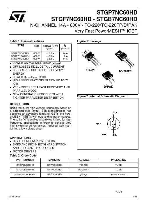
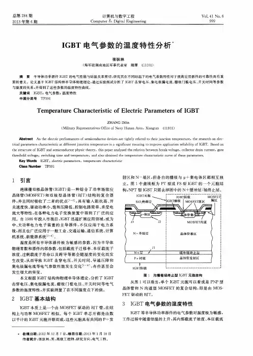
1/15June 2005STGP7NC60HDSTGF7NC60HD - STGB7NC60HDN-CHANNEL 14A - 600V - TO-220/TO-220FP/D²PAKVery Fast PowerMESH™ IGBTTable 1: General Featuress LOWER ON-VOLTAGE DROP (V cesat )s OFF LOSSES INCLUDE TAIL CURRENT sLOSSES INCLUDE DIODE RECOVERY ENERGYs LOWER C RES /C IES RATIOsHIGH FREQUENCY OPERATION UP TO 70 KHzsVERY SOFT ULTRA FAST RECOVERY ANTI PARALLEL DIODEsNEW GENERATION PRODUCTS WITH TIGHTER PARAMETER DISTRIBUTIONDESCRIPTIONUsing the latest high voltage technology based on a patented strip layout, STMicroelectronics has designed an advanced family of IGBTs, the Pow-erMESH ™ IGBTs, with outstanding performances.The suffix "H" identifies a family optimized for high frequency applications in order to achieve very high switching performances (reduced tfall) man-taining a low voltage drop.APPLICATIONSs HIGH FREQUENCY INVERTERSs SMPS AND PFC IN BOTH HARD SWITCH AND RESONANT TOPOLOGIES s MOTOR DRIVERSTable 2: Order CodeTYPE V CES V CE(sat) (Max) @25°C I C@100°CSTGP7NC60HD STGF7NC60HD STGB7NC60HD600 V 600 V 600 V< 2.5 V < 2.5 V < 2.5 V14 A 6 A 14 APART NUMBER MARKING PACKAGE PACKAGINGSTGP7NC60HD GP7NC60HD TO-220TUBE STGF7NC60HD GF7NC60HD TO-220FP TUBE STGB7NC60HDT4GB7NC60HDD 2PAKTAPE & REELRev.9STGP7NC60HD - STGF7NC60HD - STGB7NC60HD2/15Table 3: Absolute Maximum ratings( ) Pulse width limited by max. junction temperature.Table 4: Thermal DataELECTRICAL CHARACTERISTICS (T CASE =25°C UNLESS OTHERWISE SPECIFIED)Table 5: Main Parameters(#) Calculated according to the iterative formula:SymbolParameterValueUnitSTGP7NC60HD STGB7NC60HDSTGF7NC60HDV CES Collector-Emitter Voltage (V GS = 0)600V V ECR Emitter-Collector Voltage 20V V GE Gate-Emitter Voltage±20V I C Collector Current (continuous) at T C = 25°C (#)2510A I C Collector Current (continuous) at T C = 100°C (#)146A I CM ( )Collector Current (pulsed)50A I F Diode RMS Forward Current at T C = 25°C 20A P TOT Total Dissipation at T C = 25°C 8025W Derating Factor0.640.20W/°C V ISO Insulation Withstand Voltage A.C.(t = 1 sec; Tc = 25°C)--2500V T stg Storage Temperature– 55 to 150°C T jOperating Junction TemperatureMin.Typ.Max.Rthj-caseThermal Resistance Junction-caseTO-220D²PAK 1.56°C/W TO-220FP5.0°C/W Rthj-ambThermal Resistance Junction-ambient62.5°C/W T LMaximum Lead Temperature for Soldering Purpose (1.6 mm from case, for 10 sec.)300°CSymbol ParameterTest ConditionsMin.Typ.Max.Unit V BR(CES)Collector-Emitter Breakdown VoltageI C = 1 mA, V GE = 0600V I CES Collector cut-off Current (V GE = 0)V CE = Max Rating, T C = 25 °C V CE = Max Rating, T C = 125 °C 101µA mA I GES Gate-Emitter Leakage Current (V CE = 0)V GE = ± 20V , V CE = 0±100nA V GE(th)Gate Threshold Voltage V CE = V GE , I C = 250 µA 3.755.75V V CE(sat)Collector-Emitter Saturation VoltageV GE = 15V, I C = 7 AV GE = 15V, I C = 7 A, Tc= 125°C1.851.72.5V VI C T C ()T JMAX T C–R THJ C –V CESAT MAX ()T C I C,()×-------------------------------------------------------------------------------------------------=3/15STGP7NC60HD - STGF7NC60HD - STGB7NC60HDELECTRICAL CHARACTERISTICS (CONTINUED)Table 6: Dynamic(1) Pulsed: Pulse duration= 300 µs, duty cycle 1.5%Table 7: Switching OnTable 8: Switching OffTable 9: Switching Energy(2) Eon is the turn-on losses when a typical diode is used in the test circuit in figure 2. If the IGBT is offered in a package with a co-pack diode, the co-pack diode is used as external diode. IGBTs & DIODE are at the same temperature (25°C and 125°C)(3) Turn-off losses include also the tail of the collector current.Symbol ParameterTest ConditionsMin.Typ.Max.Unit g fs (1)Forward Transconductance V CE = 15 V , I C = 7 A4.30S C ies Input Capacitance V CE = 25 V, f= 1 MHz, V GE = 0720pF C oes Output Capacitance 81pF C res Reverse Transfer Capacitance17pF Q g Q ge Q gc Total Gate Charge Gate-Emitter Charge Gate-Collector Charge V CE = 390 V, I C = 7 A,V GE = 15 V (see Figure 22)3571648nC nC nC I CLTurn-Off SOA Minimum CurrentV clamp = 480 V , Tj = 150°C R G = 10 Ω, V GE = 15 V50ASymbol ParameterTest ConditionsMin.Typ.Max.Unit t d(on)t r (di/dt)on Turn-on Delay Time Current Rise Time Turn-on Current Slope V CC = 390 V, I C = 7 AR G =10 Ω, V GE = 15V, Tj= 25°C (see Figure 19)18.58.51060ns ns A/µs t d(on)t r (di/dt)onTurn-on Delay Time Current Rise Time Turn-on Current SlopeV CC = 390 V, I C = 7 AR G =10 Ω, V GE = 15V, Tj= 125°C (see Figure 20)18.571000ns ns A/µsSymbol ParameterTest ConditionsMin.Typ.Max.Unit t r (V off )Off Voltage Rise Time V cc = 390 V, I C = 7 A, R G = 10 Ω , V GE = 15 V T J = 25 °C(see Figure 20)27ns t d (off )Turn-off Delay Time 72ns t f Current Fall Time 60ns t r (V off )Off Voltage Rise Time V cc = 390 V, I C = 7 A, R G = 10 Ω , V GE = 15 V Tj = 125 °C (see Figure 20)56ns t d (off )Turn-off Delay Time 116ns t fCurrent Fall Time105nsSymbol ParameterTest ConditionsMin.Typ.Max Unit Eon (2)E off (3)E ts Turn-on Switching Losses Turn-off Switching Loss Total Switching Loss V CC = 390 V, I C = 7 AR G = 10 Ω, V GE = 15V, Tj= 25°C (see Figure 19)95115210125150275µJ µJ µJ Eon (2)E off (3)E tsTurn-on Switching Losses Turn-off Switching Loss Total Switching LossV CC = 390 V, I C = 7 AR G = 10 Ω, V GE = 15V, Tj= 125°C (see Figure 20)140215355µJ µJ µJSTGP7NC60HD - STGF7NC60HD - STGB7NC60HD4/15Table 10: Collector-Emitter DiodeSymbolParameterTest CondictionMin.Typ.Max.UnitV f Forward On-Voltage If = 3.5 AIf = 3.5 A, Tj = 125 °C 1.31.1 1.9V V t rr t a Q rr I rrm S Reverse Recovery Time Reverse Recovery Charge Reverse Recovery Current Softness factor of the diode If = 7 A, V R = 40 V,T j = 25 °C, di/dt = 100 A/µs3722402.10.68ns ns nC A t rr t a Q rr I rrm SReverse Recovery Time Reverse Recovery Charge Reverse Recovery Current Softness factor of the diodeIf = 7 A, V R = 40 V,T j = 125 °C, di/dt = 100 A/µs6134983.20.79ns ns nC ASTGP7NC60HD - STGF7NC60HD - STGB7NC60HDFigure 3: Output CharacteristicsFigure 6: Transfer Characteristics5/15STGP7NC60HD - STGF7NC60HD - STGB7NC60HD6/15Figure 9: Normalized Breakdown Voltage vsFigure 12: Gate Charge vs Gate-Emitter Volt-age7/15STGP7NC60HD - STGF7NC60HD - STGB7NC60HDFigure 15: Thermal Impedance For TO-220/Figure 17: Turn-Off SOASTGP7NC60HD - STGF7NC60HD - STGB7NC60HD Figure 19: Ic vs Frequencycations, the typical collector current vs. maximum operating frequency curve is reported. That fre-quency is defined as follows:f MAX = (P D - P C) / (E ON + E OFF)1) The maximum power dissipation is limited by maximum junction to case thermal resistance:P D = ∆T / R THJ-Cconsidering ∆T = T J - T C = 125 °C- 75 °C = 50°C2) The conduction losses are:P C = I C * V CE(SAT) * δwith 50% of duty cycle, V CESAT typical value@125°C.3) Power dissipation during ON & OFF commuta-tions is due to the switching frequency:P SW = (E ON + E OFF) * freq.4) Typical values @ 125°C for switching losses areused (test conditions: V CE = 390V, V GE = 15V,R G = 3.3 Ohm). Furthermore, diode recovery en-ergy is included in the E ON (see note 2), while thetail of the collector current is included in the E OFF measurements (see note 3).8/15STGP7NC60HD - STGF7NC60HD - STGB7NC60HDFigure 20: Test Circuit for Inductive Load SwitchingFigure 21: Switching WaveformsFigure 22: Gate Charge Test CircuitFigure 23: Diode Recovery Time Waveforms9/15STGP7NC60HD - STGF7NC60HD - STGB7NC60HD10/15TAPE AND REEL SHIPMENTD 2PAK FOOTPRINT* on sales typeDIM.mm inch MIN.MAX.MIN.MAX.A 33012.992B 1.50.059C 12.813.20.5040.520D 20.20795G 24.426.40.960 1.039N 1003.937T30.4 1.197BASE QTYBULK QTY10001000REEL MECHANICAL DATADIM.mm inch MIN.MAX.MIN.MAX.A010.510.70.4130.421B015.715.90.6180.626D 1.5 1.60.0590.063D1 1.59 1.610.0620.063E 1.65 1.850.0650.073F 11.411.60.4490.456K0 4.8 5.00.1890.197P0 3.9 4.10.1530.161P111.912.10.4680.476P2 1.9 2.10.0750.082R 50 1.574T 0.250.350.00980.0137W23.724.30.9330.956TAPE MECHANICAL DATATable 11: Revision History 9Date Revision Description of Changes 07-Jun-20044Stylesheet update. No content change19-Aug-20045Complete Version17-Sep-20046Figure 18 has been added09-Nov-20047Final datasheet19-Jan-20058Datasheet updated09-Jun-20059Modified titleInformation furnished is believed to be accurate and reliable. However, STMicroelectronics assumes no responsibility for the consequences of use of such information nor for any infringement of patents or other rights of third parties which may result from its use. No license is granted by implication or otherwise under any patent or patent rights of STMicroelectronics. Specifications mentioned in this publication are subject to change without notice. This publication supersedes and replaces all information previously supplied. STMicroelectronics products are not authorized for use as critical components in life support devices or systems without express written approval of STMicroelectronics.The ST logo is a registered trademark of STMicroelectronicsAll other names are the property of their respective owners© 2005 STMicroelectronics - All Rights ReservedSTMicroelectronics group of companiesAustralia - Belgium - Brazil - Canada - China - Czech Republic - Finland - France - Germany - Hong Kong - India - Israel - Italy - Japan - Malaysia - Malta - Morocco - Singapore - Spain - Sweden - Switzerland - United Kingdom - United States of America。
IGBT模块的寿命和可靠性研究系统寿命与可靠性关系:可靠性:产品在一定条件下无故障完成规定功能的能力或可能性IGBT模块的失效模式:功率周次 Power cycling:功率周次用于评估绑定线和Die焊层的机械寿命Power cycling can estimate the bonding wire and die solder’s lifetime π测试方法: 加载自加热,周期≤ 3秒,测试ΔTvjπ Test method: Self heating by load, T_cycle ≤ 3 seconds, measure ΔTvj π失效判据:饱和压降 Vcesat 增大+5%π Failure criteria: Vcesat increase more than 5%温度周次 Thermal cycling温度周次用于评估DCB下焊接层的寿命Thermal cycling can estimate DCB solder’s lifetimeπ测试方法: 通电加热,周期5分钟,测量ΔTcπ Test method: Self heating by l oad, 5 min/, measure ΔTc π失效判据:热阻Rthjc 增大+20%π Failure criteria: R_thjc increase 20%失效机理是两种材料不同的膨胀系数(Different material’s CTE)[ppm/K]不同应用下IGBT模块的寿命Lifetime of IGBT module in different applicationThere are many applications and similar types of power modules.Main objective is: how to select an active device in order to reach desired system lifetime?Is it possible to have power module suiting to all applications?由周期内系统工况变化获得温度变化Get the temperature profile by power profile in a cycle温度变化导致的失效模式Failure modes with ΔTThere are two key factors in the selection of the appropriate power module:1)thermal: Tvj op < Tvj max2)reliability: wear out mechanisms which determine module lifetime as result of modulereliability curves and thermal stressesNote: RBSOA and other electrical phenomena are not covered in the presentation. Factors and impacts:1)TjFWD max ≤ Tvj opTjIGBT max ≤ Tvi opNowadays Tvj op = 150°C2)DTjFWD & DTjIGBT refer to Power Cycling reliability curvesΔTC refers to Thermal Cycling reliability curvesReliability curves are always given by power module manufacturer绑定线老化——功率周次曲线Bond wire degradation – PC curve功率周次曲线修正因数PC curve correction factor基板焊层老化——热循环曲线Solder on baseplate degradation – TC curve功率温度循环(PC)次数评估计算No. of cycle estimation calculation with Power cycling curve实例:稳态周期系统的寿命估算Simple mission cycle -- example of lifetime estimationFor relative simple mission cycles the module lifetime based on the three presented reliabilitycurves and power losses converted into a junction and case temperature swing can be easilyestimated. PrimePACK™ module in use: FF900R12IP4D实例:稳态周期系统的寿命估算Simple mission cycle -- example of lifetime estimationQuestion from last page: how to estimate the power module lifetime under the mission cycle,has to be repeated again. Let’s calculate the module wear out as a function of mission cycle and time.Final lifetime module estimation:wear out / year = 0,3% + 5.8% + 4,38ppm + 8,76ppm ≌ 6.1%As reliability curves are given for 100% lifetime the module can work in the example applicationfor :100% / 6.1% ≌ 16.4yearsNote: These calculations are made for IGBT only. FWD has to be calculated separately.动态负载周期的寿命估算方法Dynamic load cycle – lifetime estimateMatlab calculates losses for given number of the load cycles and applies them to the thermal networks specific for selected module in Simulink. As a result the junction temperature profile for IGBT, Diode and the profile of the solder temperature is obtained.In that case, the simulation will be stopped. Over the graph the information says, which element has higher temperature than allowed. If its below..雨流计数法---随机负载谱转化为变幅或恒幅的负载谱•把负载变化周次种类减少•根据有限的试验数据推算整个寿命周期的变化规律,获得典型谱From the temperature profile analysis the life time (and wear of the life time in %) for each element and solder will be calculated. The graphs will show the life time wear for each deltaT. The sum of the percents is calculated and also shown on the graph.IGBT4模块的性能提升High performance of IGBT4 moduleIGBT4模块的150度最高允许工作结温,源于内部焊线工艺的改进,使其可靠性指标-功率周次(PC)数大幅增加!铜绑定线 Copper Bonding Wire-- EconoDUAL™3 600A真正实现 EconoDUAL™3 最大输出电流能力--- @ TC=100°C, Tvj=175°C降低引线电阻 R CC‘EE‘保证功率周次,满足风力发电,电动汽车需求提供焊接/PressFIT 两种兼容版本提供650V,1200V,1700V IGBT4 全系列,便于现有设计的功率升级PressFIT 端子压接技术Press + FIT = PressFITPressFIT Technology无铅以达到RoHS环保要求简易无焊接安装节约生产组装的成本和时间高可靠性减少工人焊接端子中失误导致的过温和静电损坏可靠性已在多个高端客户的产品中得到验证超声波焊接的功率端子 Ultrasonic welded terminals功率端子采用超声波焊接Internal terminal connections ultrasonic welded- 可增加模块端子的鲁棒性 Increased mechanical robustness- 可增加模块端子电流通过能力 Higher terminal currents possible- 无焊料可增加热传导能力 maximum temperature even reduced已应用在以下的模块封装中:PrimePACK, IHM-B Traction series, EconoPACK™4 模块基板和衬底材料的选择以提高温度周次。

IGBT热阻及瞬态热阻抗测试方法研究发布时间:2021-11-23T04:00:55.755Z 来源:《中国电力企业管理》2021年8月作者:郭杰、张继博、饶琼、杨钰[导读] 介绍了IGBT热阻及瞬态热阻抗的测试方法,在此基础上研制出了一种用于IGBT及FRD模块的热阻测试设备。
本测试设备采用基于LabVIEW的计算机控制技术,实现了热阻及瞬态热阻抗的计算机自动测试。
西安派瑞功率半导体变流技术有限公司郭杰、张继博、饶琼、杨钰陕西西安 710061摘要:介绍了IGBT热阻及瞬态热阻抗的测试方法,在此基础上研制出了一种用于IGBT及FRD模块的热阻测试设备。
本测试设备采用基于LabVIEW的计算机控制技术,实现了热阻及瞬态热阻抗的计算机自动测试。
关键词:IGBT 热阻及瞬态热阻抗测试 LabVIEW Research on the testing method of IGBT GUO Jie,QIAO Yu, DUAN Xin,FANG Qi Abstract:Introduce the testing method of IGBT thermal resistance and transient thermal impedance, developed a testing equipment of thermal resistance for IGBT module and FRD. The test equipment adopted computer control based on the LABVIEW platform, realized the auto-test of thermal resistance and transient thermal impedance. Keywords: IGBT;thermal resistance and transient thermal impedance;test;LabVIEW Foundation Project:Supported by national science and technology supporting research plan,A new type of power electronics device and power electronics integrate technology(No. 2007BAA12B01) 1.概述绝缘栅双极型晶体管(IGBT)是一种MOS场效应和双极型晶体管复合的新型电力电子器件。
IGBT驱动软关断和有源钳位技术【摘要】:由于功率回路杂散电感的存在,IGBT在关断过程中会产生过高的Vce电压尖峰,带来了IGBT损坏的风险。
本文介绍了PI公司在大功率驱动系统中常用的软关断和有源钳位技术,分析了两种电路抑制IGBT关断电压尖峰的基本工作原理和注意事项。
通过这两种技术可以有效减缓IGBT的di/dt,从而降低Vce电压尖峰,有效保护IGBT正常运行。
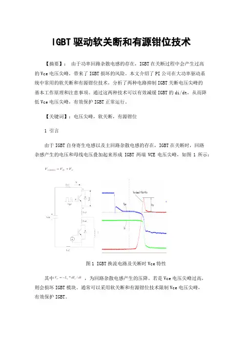
【关键词】:电压尖峰,软关断,有源钳位1 引言由于IGBT自身寄生电感以及主回路杂散电感的存在,IGBT在关断时,回路杂感产生的电压和母线电压叠加起来形成IGBT两端VCE电压尖峰,如图1所示:图1 IGBT换流电路及关断时Vce特性其中,为回路杂散电感产生的压降。
若是Vce电压尖峰过高,则会损坏IGBT模块。
通常可以采用软关断和有源钳位技术限制Vce电压尖峰,有效保护IGBT。
1.解决分析过程1.软关断技术软关断技术基本工作原理:如图2所示,IGBT正常关断时,选择较小的门极关断电阻以减少开关损耗;当检测到短路故障时,切换到较大的关断电阻缓慢释放门极电荷,减缓门极电压下降速度,从而减小IGBT的di/dt,降低Vce电压尖峰。
图2 IGBT软关断原理示意图图3所示为驱动板检测到IGBT短路时的软关断保护试验波形,可以看到通过软关断,电流缓慢降低,产生的Vce电压尖峰也很小,有效保护了IGBT。
图3驱动板检测到短路保护故障然而软关断电路需要检测到短路故障才能动作,这一条件在一定程度上限制了软关断的可靠性。
具体分析如下:如图4所示IGBT的开通特性,短路保护是根据IGBT开通后经过一段响应时间检测到的Vce是否大于短路门槛电压Vth反馈的。
当检测到的Vce大于Vth,则认定为短路故障;反之,正常运行。
图4 IGBT开通特性及Vce检测若是在短路情况下,是一个宽度小于响应时间的脉冲驱动信号,将检测不到短路状况,不能执行软关断,将会产生过高的Vce电压,可能损坏IGBT。
移相全桥和L L C技术在电推进PPU上的应用对比陈昶文,武桐,冯玮玮,张保平(兰州空间技术物理研宄所,甘肃兰州73_)摘要:分别采用移相全桥和全桥LLC设计了离子电推进电源处理单元(PPU)屏栅电源模块。
针对恒流启动、打 火保护、负载调整率等特性开展了设计和实验验证。
得出移相全桥变换器应用在P PU设计显著提高了效率,但 整流二极管和变压器绕组的电压应力较髙,限制了单模块能够输出的最大电压;全桥LLC变换器消除了输出端滤波电感和箝位电路,降低了绝缘设计的难度和体积重量,劣势在于在输入电压范围变宽时效率下降明显。
关键词:电源处理单元;电推进;移相全桥中图分类号:V423.4+4 文献标识码:A 文章编号:1000-100X(2021)05-0053-04Comparison of Phase-shifted Full Bridge and LLC Technology inElectric Propulsion PPUCHEN Chang-wen,W U Tong,FENG Wei-wei,ZHANG Bao-ping(Lanzhou Institute of Space Technology Physics, Lanzhou73C X X X), China)Abstract : The grid power module of power processing unit (PPU) is designed by using phase-shifted full bridge and full bridge LLC respectively.The constant current start-up, ignition protection and load regulation are designed and verified by experiments.lt is concluded that the phase-shifting full bridge converter can significantly improve the efficiency of PPU, but the voltage stress of rectifier diode and transformer winding is high, which limits the maximum output voltage of a single module, the full bridge LLC converter eliminates the filter inductance and clamp circuit at the output end,reduces the difficulty and volume weight of the insulation design,but the disadvantage is that the efficiency decreases when the input voltage range is widened obviously.Keywords : power processing unit; electric propulsion; phase-shifting full bridgel引言屏栅电源及阳极电源分别是离子电推进和霍 尔电推进PPU中的核心模块,处理了对应P P U 80% 以上的功率屏栅和阳极电源输出电压高、处 理功率大,高效率变换是其热设计和可靠性设计的 关键。
Comparison of Press-Pack IGBT at Hard Switching and Clamp Operation for Medium Voltage ConvertersRodrigo Alvarez,Felipe Filsecker,Steffen BernetTechnische Universitaet DresdenHelmholzstrasse9Dresden,GermanyEmail:Rodrigo.alvarez@mailbox.tu-dresden.deKeywords<<IGBT>>,<<Device characterization>>,<<Test bench>>,<<Packaging>>,<<Device application>> and<<Industrial application>>.AbstractThe newly developed press-pack IGBT devices compete with IGCTs in high power industrial applica-tions.These new semiconductors were already studied in detail for hard switching[1]and for clamp operation[2].Nevertheless,a comparison of the basic switching characteristics of the IGBT press-pack devices for hard switching and clamp operation has not been done so far.This paper compares the switching behavior,the switching losses and the safe operating area trajectoriesof the new85mm,4.5kV,1.2kA press-pack SPT+IGBT for hard switching and clamp operation.The methods used for the experimental characterization and comparison are explained in detail.IntroductionNowadays medium voltage converters are essential for the application areas industry,traction,marineand energy.They increase the efficiency of processes,allowing better control of the energyflow.Power semiconductors are the basic building block of medium voltage converters,and their development has enabled a substantial improvement of the converter technology during the last years[3–5].Up to now,IGBT modules and IGCT press pack devices have shared the market of self commutated medium voltage converters.Recent trends suggest that self-commutated converters will be the dominating technology for applications below30MV A in the middle term[6,7].Press-pack IGBTs combine the advantages of IGBT dies with those of press-pack housing,making theman attractive alternative to IGCTs[8–11].The static and switching behavior of the new85mm,4.5kV,1.2kA press-pack SPT+IGBT at hard switching was described in[1].Reference[2]proposes the useof a clamp circuit for the aforementioned IGBT.An IGBT press pack device offers the potential of ahigh power cycling capability,an explosion free converter design,and low switching and total losses. Obviously,the IGBT press pack devices have become an interesting alternative to IGCTs in high power medium voltage applications.[8,10]This paper presents a detailed comparison of the switching behavior,the switching losses and the semi-conductor stress of both modes of operation for diverse collector currents and junction temperatures.Semiconductor Data and Test BenchFor the comparison of the switching behavior and switching losses of the new4.5kV,1.2kA press-pack Soft-Punch-Through Plus(SPT+)IGBT T1200EB45E four configurations have been tested:•Hard Switching with a stray inductance of120nH•Clamp1with L cl-1=1µH•Clamp2with L cl-2=2µH•Clamp3with L cl-3=5.6µHTable I:Semiconductor dataDevice Diode IGBTManufacturer Infineon WestcodeModel D1031SH T1200EB45EDiameter62.8mm85mmSi-area3097mm24284mm2Active Si-area A aSi2463mm22142mm2R thJH(2sides)14.1K/kW9K/kWTable II:Semiconductor core valuesDiode IGBTV RRM4500V V CES4500VI FRMSM2300A V DC-link2800VI FA VM1470A I C(DC)2132AI RM1500A I C(nom)1200AC(a)C(b)Figure1:Test bench schematic diagram for(a)hard switching and for(b)soft switching with clamp circuit The test setup includes the diode D1031SH as freewheeling diode D f as well as clamp diode D cl,and the commercially available gate unit C0030BG400(R G,on=3.3Ωand R G,off=2.2Ω).The semiconductor data are summarized in Tables I and II.The test bench schematic diagram for the different operation modes is shown in Fig.1.The clamp circuit design is detailed in Table III.The test circuit is a buck converter,which allows the study of the switching behavior of an active switch (e.g.IGBT,IGCT)and its corresponding freewheeling diode through the use of a double-pulse switching pattern[3].The dc-link was buffered near to the stack by an extra capacitor C stb(220µF)in order toTable III:Test bench and current snubber setupTest bench Clamp circuitC dc 4.5mF C cl10µFC stb220µF R cl0.5ΩL Load1mH L cl1,2,5.6µHV dc 2.5kV(a)(b)Figure2:Experimental setup(a)IGBT stack for hard switching,(b)stack with clamp circuit achieve a low stray inductance.A robust mechanical design was accomplished using2mm-thick copper plates connecting the dc-link capacitor C dc,the additional buffer capacitor C stb and the stack.Thus,the mechanical construction of the test bench is able to withstand short circuit currents of about200kA in case of a device failure.The two diodes D prot limit possible negative voltages across the dc-link capacitor,preventing an oscillation of the short circuit current and the fuse F avoids the complete discharge of the dc-link capacitors through the stack in failure case limiting the maximum short circuit current to value of less than60kA.These are two important components of the safety concept of the test bench.The junction temperatures of the devices are adjusted by two ring heaters mounted in the stack,control-ling the case temperature[3].The dc-link capacitor is charged by a high-voltage power supply before the measurements are carried out.A partially automated measurement system was used.The values of V dc and I L are set using a LabVIEW program on a PC connected to the test bench by opticalfiber cables. The measurements are captured by two8bit four-channel digital oscilloscopes(Tektronix TDS714L), capable of working at a500MS/s sample rate.The storage and analysis of the data is carried out on an extra computer.The experimental setup is shown in Fig.2.Comparison of4.5kV,1.2kA Press-Pack IGBT at Hard Switching and Clamp OperationThe press-pack IGBT was characterized for hard switching and clamp operation for different gate resis-tances R G,collector currents i C,dc-link voltages V dc and junction temperatures T j,as Table IV shows. Hard switching and clamp operation are compared regarding the stress in the safe operating area(SOA), peak power,semiconductor switching losses and clamp switching losses.The definitions of the quantities used for the calculations(e.g.d i/dt,d v/dt)correspond with those presented in[1,2].Comparison of SOA Trajectories and Maximum Instantaneous PowerThe press-pack IGBT and the freewheeling diode feature a smooth switching behavior in all investigated operating points.Waveforms of device voltages,currents and instantaneous power as well as SOA tra-jectories at V dc=2.5kV,i C=1.2kA,T j=125◦C and the lowest recommended gate resistance illustrate the behavior of the semiconductors for the selected hard switching and clamp operation(Figs.3to5).(a)(b)(c)Figure3:IGBT turn-off behavior(a)waveforms,(b)peak power,(c)Safe Operating Area trajectories(T j=125◦C, V DC=2.5kV and i C=1.2kA)(a)(b)(c)Figure4:IGBT turn-on behavior(a)waveforms,(b)peak power,(c)Safe Operating Area trajectories(T j=125◦C, V DC=2.5kV and i C=1.2kA)Table IV:Conducted measurementsHard SwitchingVariable ValueV dc2000and2500Vi L100,300,600,900,1200,1500and1800AT j25,60,90,125◦CLσ120and210nHR G,on-1...3 3.3,5.6and6.8ΩR G,off-1...3 2.2,3.6and6.8ΩClamp OperationVariable ValueV dc2000and2500Vi L100,300,600,900,1200,1500and1800AT j25,60,90,125◦CL cl1,2,3 1.0,2.0and5.6µHThe turn-off behavior of the IGBT is almost not influenced by the different clamp configurations,con-firming the adequate selection of the clamp components.The clamp inductance L cl induces a small overvoltage caused by the demagnetization(Fig.3a),which does not affect the peak power(Fig.3b),but slightly increases the turn-off losses by about8%compared to hard switching.The clamp inductance has a remarkable influence on the turn-on transient,changing the d i C/dt from 4.2kA/µs for GU-1(R G,on-1=3.3Ωand R G,on-1=2.2Ω)at hard switching to0.5kA/µs for operation with L cl-3,keeping d v CE/dt at roughly3.5kV/µs(Fig.4a).Moreover,the clamp reduces the turn-on stress of the IGBT in contrast to hard switching:the collector current i C rises with a low device voltage, which reduces the IGBT turn-on peak power by approximately95%from5.15MW for hard switching to0.23MW for L cl-3=5.6µH(Fig.4b).The turn-on SOA traces of the clamp-operated IGBTs show a substantially larger distance to the SOA margins than the IGBT at hard switching(Fig.4c).Obviously, the maximum collector current i C at IGBT turn-on is smaller for IGBTs at clamp operation,due to the reduction of d i C/dt,which also affects the reverse-recovery behavior and losses of the corresponding freewheeling diode.As expected for the diode,the reverse recovery current is reduced as the clamp inductance L cl is in-creased,see Fig.5a(a lower d i D/dt reduces the reverse recovery charge).Accordingly,the diode presents the highest stress for the operation with clamp1(L cl-1),caused by the larger voltage peak generated through the combination of a still considerable d i D/dt and the relatively large stray inductance of the clamp circuit configuration(Fig.5b).An increase of L cl reduces the d i D/dt,the peak reverse recovery current and the rate of current change of the decrease of the reverse recovery current.Thus,the instanta-neous peak power decreases for L cl-2and L cl-3.The diode turn-off SOA traces show that the hard switching operation approaches to the i D margins of the SOA,whereas the clamp operation increases the distance to this limit,but reduces the distance to the diode voltage v D limit(Fig.5c).The diode presents maximum stress at turn-off transients;the clamp configuration can reduce or increase this stress depending on the relation between clamp inductance, stray inductance,peak reverse recovery current and rate of change of the decrease of the reverse recovery current.A poor design can generate large diode voltage peaks,increasing the stress of the diode.For the studied operating points,the press-pack IGBT is subject to the largest stress at hard switching during turn-on,and with clamp operation during turn-off transients.The maximum stress is reduced by about40%compared to hard switching,due to the addition of a clamp circuit.Comparison of LossesThe main goal of the use of the clamp configuration is the reduction of the IGBT switching losses.Of course also the diode losses and the total converter losses should not increase compared to hard switching. The semiconductor switching losses of IGBT and diode(E sw,SC)are defined as:E sw,SC=E on,IGBT+E off,IGBT+E off,Diode(1) withE on,IGBT:IGBT turn-on switching lossesE off,IGBT:IGBT turn-off switching losses(a)(b)(c)Figure 5:Diode turn-off behavior (a)waveforms,(b)peak power,(c)Safe Operating Area trajectories (T j =125◦C,V DC =2.5kV and i C =1.2kA)E off,Diode :Diode turn-off switching lossesIn case of clamp operation,the clamp losses are calculated by (2),which includes the losses of the clamp diode E D,cl and clamp resistor E R,cl .Stationary losses of the clamp inductor (caused by the parasitic ohmic resistance)and the clamp capacitor (caused by the equivalent parallel resistance)are neglected.E cl =E D,cl +E R,cl(2)The sum of the semiconductor and clamp switching losses of the four selected configurations were com-pared at V dc =2.5kV ,T j =125◦C and i C =600and 1200A.The results can be seen in Fig.6.The values on top of the columns are the sum of the semiconductor and clamp switching losses (E sw,SC+cl )and the values in parentheses are the semiconductor switching losses.The semiconductor switching losses were reduced by 13to 30%(clamp 1to 3respectively)for clamp operation compared to hard switching.The largest loss reduction by the clamp circuit was achieved during IGBT turn-on.However,the sum of the semiconductor and clamp switching losses were reduced by less than 3%at 600A and less than 11%at 1200A ,which means that a major part of the turn-on losses are transferred from the IGBT to the clamp resistance R cl .The larger reduction of the semiconductor switching losses is achieved by L cl-3.However,the selection of a clamp should consider the stress of the semiconductors,both switching and clamp losses and particular specifications for the application (e.g.d v /dt,power density,reliability,mounting cost,etc.).For example,in the studied cases,clamp 2presents a good trade off between a reduction of semicon-ductor switching losses,clamp switching losses and stress of the diode.The diode stress is increased marginally (3.37%),achieving a reduction of the semiconductor switching losses of 25%and a reduc-tion of the semiconductor and clamp switching losses of 8%.This allows the reduction of the cooling system or a higher converter output power.However,finally an optimum for criteria like volume,weight,efficiency and costs must be found.The realization of a clamp seems to be an interesting option.Figure6:Semiconductor and clamp switching losses(V dc=2.5kV,T j=125◦C,left i C=600A,right i C=1200A) ConclusionsThis paper shows a detailed comparison of the switching behavior and switching losses of the press-pack IGBT T1200EB45E at hard switching and clamp operation.It shows that the use of clamp circuits for press-pack IGBTs features interesting characteristics like reduced switching losses(up to30%)and less stress of the semiconductors(lower d i C/dt,reverse recovery current and peak power for IGBT and diode). The optimum clamp circuit will depend on the specification requirements of the particular application. The saved semiconductor switching losses enable an increase of the converter power or switching fre-quency in medium voltage converters,since both characteristics are limited thermally by the semicon-ductor losses and the cooling configuration.It is remarkable that the sum of switching and clamp losses are lower than at hard switching.For example the sum of switching and clamp losses are reduced by about3%at50%and11%at100%rated current.References[1]R.Alvarez,F.Filsecker,and S.Bernet,“Characterization of a new4.5kV press pack SPT+IGBTfor medium voltage converters,”in Energy Conversion Congress and Exposition,2009.ECCE 2009.IEEE,San Jose,USA,Sept.2009,pp.3954–3962.[2]R.Alvarez,S.Bernet,L.Lindenmueller,and F.Filsecker,“Characterization of a new4.5kV presspack SPT+IGBT in voltage source converters with clamp circuit,”in Industrial Technology,2010.ICIT2010.IEEE International Conference on,Vi˜n a del Mar,Chile,March2010.[3]S.Tschirley and S.Bernet,“Automated testing of high power semiconductor devices,”in Proc.PELINCEC2005,Warsaw,Poland,2005.[4]J.Rodriguez,S.Bernet,B.Wu,J.Pontt,and S.Kouro,“Multilevel voltage-source-converter topolo-gies for industrial medium-voltage drives,”IEEE Trans.on Industrial Electron.,vol.54,no.6,pp.2930–2945,Dec.2007.[5]S.Bernet,“Recent developments of high power converters for industry and traction applications,”IEEE Trans.on Power Electron.,vol.15,no.6,pp.1102–1117,Nov2000.[6]B.Bose,“Evaluation of modern power semiconductor devices and future trends of converters,”Industry Applications,IEEE Transactions on,vol.28,no.2,pp.403–413,Mar/Apr1992.[7]M.Hiller,R.Sommer,and M.Beuermann,“Converter topologies and power semiconductors forindustrial medium voltage converters,”in Industry Applications Society Annual Meeting,2008.IAS ’08.IEEE,Edmonton,Alberta,Canada,Oct.2008,pp.1–8.[8]F.Wakeman,G.Li,and A.Golland,“New family of4.5kV press-pack IGBTs,”in Proceedings ofPCIM Europe2005,Nuremberg,Germany,June2005.[9]A.Morozumi,K.Yamada,T.Miyasaka,S.Sumi,and Y.Seki,“Reliability of power cycling forIGBT power semiconductor modules,”Industry Applications,IEEE Transactions on,vol.39,no.3, pp.665–671,May-June2003.[10]M.Rahimo and S.Klaka,“High voltage semiconductor technologies,”in Power Electronics andApplications,2009.EPE’09.13th European Conference on,Barcelona,Spain,Sept.2009,pp.1–10.[11]E.Carroll,“High-power active devices,”ABB Switzerland,2004.。