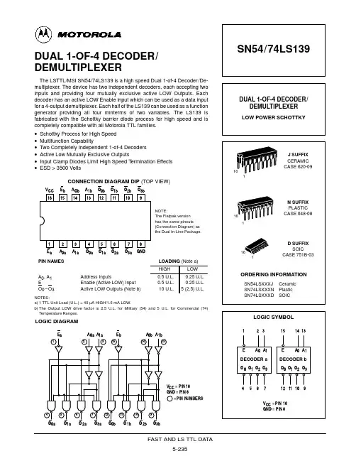
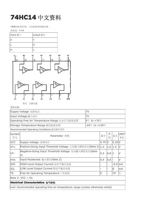
SN74HC139DRG4中文资料
- 格式:pdf
- 大小:663.14 KB
- 文档页数:18
SN54HC139, SN74HC139DUAL 2ĆLINE TO 4ĆLINE DECODERS/DEMULTIPLEXERS
SCLS108D − DECEMBER 1982 − REVISED SEPTEMBER 2003
1POST OFFICE BOX 655303 • DALLAS, TEXAS 75265
DTargeted Specifically for High-Speed
Memory Decoders and Data-TransmissionSystemsDWide Operating Voltage Range of 2 V to 6 V
DOutputs Can Drive Up To 10 LSTTL Loads
DLow Power Consumption, 80-µA Max I
CC
DTypical t
pd = 10 ns
D±4-mA Output Drive at 5 V
DLow Input Current of 1 µA Max
DIncorporate Two Enable Inputs to Simplify
Cascading and/or Data Reception
description/ordering informationThe ’HC139 devices are designed forhigh-performance memory-decoding ordata-routing applications requiring very shortpropagation delay times. In high-performancememory systems, these decoders can minimizethe effects of system decoding. When employedwith high-speed memories utilizing a fast enablecircuit, the delay time of these decoders and theenable time of the memory usually are less thanthe typical access time of the memory. This meansthat the effective system delay introduced by thedecoders is negligible.
ORDERING INFORMATIONTAPACKAGE†PACKAGE†ORDERABLEPART NUMBERTOP-SIDEMARKING
PDIP − NTube of 25SN74HC139NSN74HC139NTube of 40SN74HC139DReel of 2500SN74HC139DRSOIC − DReel of 250SN74HC139DTHC139
°°SOP − NSReel of 2000SN74HC139NSRHC139−40C to 85CSSOP − DBReel of 2000SN74HC139DBRHC139Tube of 90SN74HC139PWReel of 2000SN74HC139PWRTSSOP − PWReel of 250SN74HC139PWTHC139
CDIP − JTube of 25SNJ54HC139JSNJ54HC139J°°CFP − WTube of 150SNJ54HC139WSNJ54HC139W−55C to 125CLCCC − FKTube of 55SNJ54HC139FKSNJ54HC139FK†Package drawings, standard packing quantities, thermal data, symbolization, and PCB design guidelines are
available at www.ti.com/sc/package.
Please be aware that an important notice concerning availability, standard warranty, and use in critical applications ofTexasInstruments semiconductor products and disclaimers thereto appears at the end of this data sheet.
32120199101112134
5678
1817161514
2A2BNC2Y02Y1
1B1Y0NC1Y11Y2
1A1GNC2Y32Y2V2G
1Y3GND
NC
SN54HC139...FK PACKAGE(TOP VIEW)
CC
NC − No internal connection
12345678161514131211109
1G1A1B1Y01Y11Y21Y3GNDVCC2G2A2B2Y02Y12Y22Y3
SN54HC139...J OR W PACKAGESN74HC139...D, DB, N, NS, OR PW PACKAGE(TOP VIEW)
Copyright 2003, Texas Instruments IncorporatedPRODUCTION DATA information is current as of publication date.
Products conform to specifications per the terms of Texas Instrumentsstandard warranty. Production processing does not necessarily includetesting of all parameters.
On products compliant to MILĆPRFĆ38535, all parameters are tested
unless otherwise noted. On all other products, productionprocessing does not necessarily include testing of all parameters.
元器件交易网www.cecb2b.comSN54HC139, SN74HC139DUAL 2ĆLINE TO 4ĆLINE DECODERS/DEMULTIPLEXERS
SCLS108D − DECEMBER 1982 − REVISED SEPTEMBER 2003
2POST OFFICE BOX 655303 • DALLAS, TEXAS 75265
description/ordering information (continued)The ’HC139 devices comprise two individual 2-line to 4-line decoders in a single package. The active-low enable(G) input can be used as a data line in demultiplexing applications. These decoders/demultiplexers feature fullybuffered inputs, each of which represents only one normalized load to its driving circuit.
FUNCTION TABLEINPUTSSELECTOUTPUTS
GBAY0Y1Y2Y3
HXXHHHHLLLLHHHLLHHLHHLHLHHLHLHHHHHL
logic diagram (positive logic)
1G1Y0
1Y11Y21Y32Y02Y12Y22Y3
1A1B
2G2A2BPin numbers shown are for the D, DB, J, N, NS, PW, and W packages.
123
151413
45671211109
元器件交易网www.cecb2b.comSN54HC139, SN74HC139DUAL 2ĆLINE TO 4ĆLINE DECODERS/DEMULTIPLEXERS
SCLS108D − DECEMBER 1982 − REVISED SEPTEMBER 2003
3POST OFFICE BOX 655303 • DALLAS, TEXAS 75265
absolute maximum ratings over operating free-air temperature range (unless otherwise noted)†Supply voltage range, VCC −0.5 V to 7 V. . . . . . . . . . . . . . . . . . . . . . . . . . . . . . . . . . . . . . . . . . . . . . . . . . . . . . . . . . Input clamp current, IIK (VI < 0 or VI > VCC) (see Note 1) ±20 mA. . . . . . . . . . . . . . . . . . . . . . . . . . . . . . . . . . . .
Output clamp current, IOK (VO < 0 or VO > VCC) (see Note 1) ±20 mA. . . . . . . . . . . . . . . . . . . . . . . . . . . . . . . . Continuous output current, IO (VO = 0 to VCC) ±25 mA. . . . . . . . . . . . . . . . . . . . . . . . . . . . . . . . . . . . . . . . . . . . . . Continuous current through VCC or GND ±50 mA. . . . . . . . . . . . . . . . . . . . . . . . . . . . . . . . . . . . . . . . . . . . . . . . . . . Package thermal impedance, θJA (see Note 2):D package 73°C/W. . . . . . . . . . . . . . . . . . . . . . . . . . . . . . . . . . .