
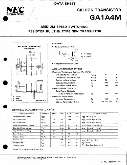
GA1A4M中文资料
- 格式:pdf
- 大小:192.65 KB
- 文档页数:4

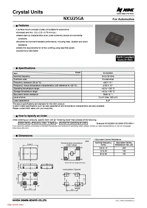

FM24C04A-G中文资料This product conforms to specifications per the terms of the Ramtron Ramtron International Corporationstandard warranty. The product has completed Ramtron’s internal1850 Ramtron Drive, Colorado Springs, CO 80921FM24C04A4Kb FRAM Serial MemoryFeatures4K bit Ferroelectric Nonvolatile RAM ? Organized as 512 x 8 bitsHigh Endurance 1012 Read/Writes ? 45 Year Data Retention ? NoDelay? WritesAdvanced High-Reliability Ferroelectric ProcessFast Two-wire Serial InterfaceUp to 1 MHz maximum bus frequency ? Direct hardware replacement for EEPROMLow Power Operation ? 5V operation150 μA Active Current (100 kHz) ? 10 μA Standby CurrentIndustry Standard ConfigurationIndustrial Temperature -40° C to +85° C ? 8-pin SOIC (-S)“Green” 8-pin SOIC (-G)DescriptionThe FM24C04A is a 4-kilobit nonvolatile memory employingan advanced ferroelectric process. A ferroelectric random access memory or FRAM is nonvolatile and performs reads and writes like a RAM. It provides reliable data retention for 45 years while eliminating the complexities, overhead, and system level reliability problems caused by EEPROM and other nonvolatile memories.Unlike serial EEPROMs, the FM24C04A performs write operations at bus speed. No write delays are incurred. Data is written to the memory array in the cycle after it has been successfully transferred to the device. The next bus cycle may commence immediately.These capabilities make the FM24C04A ideal for nonvolatile memory applications requiring frequent or rapid writes. Examples range from data collection where the number of write cycles may be critical, to demanding industrial controls where the long write time of EEPROM can cause data loss. The combination of features allows more frequent data writing with reduced overhead for the system.The FM24C04A provides substantial benefits to users of serial EEPROM, yet these benefits are available in a hardware drop-in replacement. The FM24C04A is available in industry standard 8-pin packages using a two-wire protocol. The specifications are guaranteed over an industrial temperature range of -40°C to +85°C.Pin ConfigurationPin Names Function A1-A2 Device Select Address 1 and 2 SDA Serial Data/Address SCL Serial Clock WP Write Protect VSS Ground VDD Supply Voltage 5VOrdering InformationFM24C04A-S 8-pin SOIC FM24C04A-G “Green” 8-pin SOICNC A1A2VSS VDD WP SCL SDAFigure 3. Data Transfer ProtocolStop ConditionA Stop condition is indicated when the bus master drives SDA from low to high while the SCL signal is high. All operationsmust end with a Stop condition. If an operation is pending when a stop is asserted, the operation will be aborted. The master must have control of SDA (not a memory read) in order to assert a Stop condition.Start ConditionA Start condition is indicated when the bus master drives SDA from high to low while the SCL signal is high. All read and write transactions begin with a Start condition. An operation in progress can be aborted by asserting a Start condition at any time. Aborting an operation using the Start condition will ready the FM24C04A for a new operation.If during operation the power supply drops below the specified V DD minimum, the system should issue a Start condition prior to performing another operation. Data/Address TransferAll data transfers (including addresses) take place while the SCL signal is high. Except under the two conditions described above, the SDA signal should not change state while SCL is high.AcknowledgeThe Acknowledge takes place after the 8th data bit has been transferred in any transaction. During this state the transmitter should release the SDA bus to allow the receiver to drive it. The receiver drives the SDA signal low to acknowledge receipt of the byte. If the receiver does not drive SDA low, the condition is a No-Acknowledge and the operation is aborted.The receiver could fail to acknowledge for two distinct reasons. First, if a byte transfer fails, the No-Acknowledge ends the current operation so that the device can be addressed again. This allows the last byte to be recovered in the event of a communication error. Second and most common, the receiverdoes not acknowledge the data to deliberately end an operation. For example, during a read operation, the FM24C04A will continue to place data onto the bus as long as the receiver sends acknowledges (and clocks). When a read operation is complete and no more data is needed, the receiver must not acknowledge the last byte. If the receiver acknowledges the last byte, this will cause the FM24C04A to attempt to drive the bus on the next clock while the master is sending a new command such as a Stop command.Slave AddressThe first byte that the FM24C04A expects after a start condition is the slave address. As shown in Figure 4, the slave address contains the device type, the device select, the page of memory to be accessed, and a bit that specifies if the transaction is a read or a write.Bits 7-4 are the device type and should be set to 1010b for the FM24C04A. The device type allows other types of functions to reside on the 2-wire bus within an identical address range. Bits 3-2 are the device address. If bit 3 matches the A2 pin and bit 2 matches the A1 pin, the device will be selected. Bit 1 is the page select. It specifies the 256-byte block of memory that is targeted for the current operation. Bit 0 is the read/write bit. A 0 indicates a write operation.Word AddressAfter the FM24C04A (as receiver) acknowledges the slave ID, the master will place the word address on the bus for a write operation. The word address is the lower 8-bits of the address to be combined with the 1-bit page select to specify exactly the byte to be written. The complete 9-bit address is latched internally.Figure 4. Slave AddressNo word address occurs for a read operation. Reads always use the lower 8-bits that are held internally in the address latch and the 9th address bit is part of the slave address. Reads always begin at the address following the previous access. A random read address can be loaded by doing a write operation as explained below.After transmission of each data byte, just prior to the acknowledge, the FM24C04A increments the internal address latch. This allows the next sequential byte to be accessed with no additional addressing. After the last address (1FFh) is reached, the address latch will roll over to 000h. There is no limit to the number of bytes that can be accessed with a single read or write operation.Data TransferAfter all address information has been transmitted, data transfer between the bus master and the FM24C04A can begin. For a read operation the FM24C04A will place 8 data bits on the bus then wait for an acknowledge. If the acknowledge occurs, the next sequential byte will be transferred. If the acknowledge is not sent, the read operation is concluded. For a write operation, the FM24C04A will accept 8 data bits from the master then send an acknowledge. All data transfer occurs MSB (most significant bit) first. Memory OperationThe FM24C04A is designed to operate in a manner very similar to other 2-wire interface memory products. The major differences result from the higher performance write capability of FRAM technology. These improvements result in some differences between the FM24C04A and a similar configuration EEPROM during writes. The complete operation for both writes and reads is explained below.Write OperationAll writes begin with a slave address then a word address. The bus master indicates a write operation by setting the LSB of the Slave address to a 0. After addressing, the bus master sends each byte of data to the memory and the memory generates an acknowledge condition. Any number of sequential bytes may be written. If the end of the address range is reached internally, the address counter will wrap from 1FFh to 000h.Unlike other nonvolatile memory technologies, there is no write delay with FRAM. The entire memory cycle occurs in less time than a single bus clock. Therefore any operation including read or write can begin immediately following a write. Acknowledge polling, a technique used with EEPROMs to determine if a write is complete is unnecessary and will always return a done condition.An actual memory array write occurs after the 8th data bit is transferred. It will be complete before the acknowledge is sent. Therefore if the user desires to abort a write without altering the memory contents, this should be done using a start or stop condition prior to the 8th data bit. The FM24C04A needs no page buffering.Pulling write protect high will disable writes to the entire array. The FM24C04A will not acknowledge data bytes that are applied to the device when write protect is asserted. In addition, the address counter will not increment if writes are attempted. Pulling WP low (V SS) will deactivate this feature.Figures 5 and 6 illustrate single-byte and multiple-byte writes.。
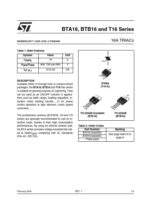
®1/9Table 1: Main FeaturesDESCRIPTIONAvailable either in through-hole or surface-mount packages, the BTA16, BTB16 and T16 triac series is suitable for general purpose AC switching. They can be used as an ON/OFF function in applica-tions such as static relays, heating regulation, in-duction motor starting circuits... or for phase control operation in light dimmers, motor speed controllers, ...The snubberless versions (BTA/BTB...W and T16series) are specially recommended for use on in-ductive loads, thanks to their high commutation performances. By using an internal ceramic pad,the BTA series provides voltage insulated tab (rat-ed at 2500V RMS ) complying with UL standards (File ref.: E81734).Symbol Value Unit I T(RMS)16A V DRM /V RRM 600, 700 and 800V I GT (Q 1)10 to 50mABTA16, BTB16 and T16 Series16A TRIAC SREV. 7February 2006SNUBBERLESS™, LOGIC LEVEL & STANDARDTable 2: Order CodesPart Number Marking BTA16-xxxxxRG See page table 8 onpage 8BTB16-xxxxxRG T16xx-xxxGBTA16, BTB16 and T16 Series2/9Table 3: Absolute Maximum Ratings Tables 4: Electrical Characteristics (T j = 25°C, unless otherwise specified)■SNUBBERLESS and Logic Level (3 quadrants)Symbol ParameterValue Unit I T(RMS)RMS on-state current (full sine wave)D 2PAK /TO-220AB T c = 100°C 16ATO-220AB Ins.T c = 15°C I TSM Non repetitive surge peak on-state current (full cycle, T j initial = 25°C) F = 50 Hz t = 20 ms 160A F = 60 Hz t = 16.7 ms168I ²t I ²t Value for fusingt p = 10 ms 144A ²s dI/dtCritical rate of rise of on-state cur-rent I G = 2 x I GT , t r ≤ 100 nsF = 120 HzT j = 125°C 50A/µs V DSM /V RSM Non repetitive surge peak off-state voltaget p = 10 msT j = 25°C V DSM /V RSM + 100V I GM Peak gate currentt p = 20 µsT j = 125°C 4A P G(AV)Average gate power dissipation T j = 125°C1W T stg T jStorage junction temperature range Operating junction temperature range- 40 to + 150- 40 to + 125°CSymbol Test ConditionsQuadrant T16BTA16 / BTB16Unit T1635SW CW BW I GT (1)V D = 12 V R L = 33 ΩI - II - III MAX.35103550mA V GT I - II - III MAX. 1.3V V GD V D = V DRM R L = 3.3 k ΩT j = 125°C I - II - IIIMIN.0.2V I H (2)I T = 500 mA MAX.35153550mA I L I G = 1.2 I GTI - III MAX.50255070mA II60306080dV/dt (2)V D = 67 %V DRM gate open T j = 125°C MIN.500405001000V/µs(dI/dt)c (2)(dV/dt)c = 0.1 V/µsT j = 125°C MIN.-8.5--A/ms(dV/dt)c = 10 V/µsT j = 125°C - 3.0--Without snubberT j = 125°C8.5-8.514BTA16, BTB16 and T16 Series3/9■Standard (4 quadrants)Table 5: Static Characteristics Table 6: Thermal resistance Symbol Test ConditionsQuadrant BTA16 / BTB16Unit C B I GT (1)V D = 12 V R L = 33 ΩI - II - III IV MAX.255050100mA V GT ALL MAX. 1.3V V GD V D = V DRM R L = 3.3 k Ω T j = 125°C ALLMIN.0.2V I H (2)I T = 500 mA MAX.2550mA I L I G = 1.2 I GTI - III - IVMAX.4060mA II 80120dV/dt (2)V D = 67 %V DRM gate openT j = 125°C MIN.200400V/µs (dV/dt)c (2)(dI/dt)c = 7 A/ms T j = 125°CMIN.510V/µsSymbol Test ConditionsValue Unit V T (2)I TM = 22.5 A t p = 380 µs T j = 25°C MAX. 1.55V V to (2)Threshold voltage T j = 125°C MAX.0.85V R d (2)Dynamic resistance T j = 125°C MAX.25m ΩI DRM I RRMV DRM = V RRMT j = 25°C MAX.5µA T j = 125°C2mANote 1: minimum I GT is guaranted at 5% of I GT max.Note 2: for both polarities of A2 referenced to A1.Symbol ParameterValue Unit R th(j-c)Junction to case (AC)D 2PAK / TO-220AB 1.2°C/WTO-220AB Insulated 2.1R th(j-a)Junction to ambient S = 1 cm ²D 2PAK45°C/WTO-220AB / TO-220AB Insulated60S = Copper surface under tab.BTA16, BTB16 and T16 Series4/9Figure 1: Maximum power dissipation versus RMS on-state current (full cycle)Figure 2: RMS on-state current versus case temperature (full cycle)Figure 3: RMS on-state current versus ambient temperature (printed circuit board FR4, copper thickness: 35µm) (full cycle)Figure 4: Relative variation of thermal impedance versus pulse durationFigure 5: On-state characteristics (maximum values)Figure 6: Surge peak on-state current versus number of cyclesBTA16, BTB16 and T16 Series5/9Figure 7: Non-repetitive surge peak on-state current for a sinusoidal pulse with width t p < 10 ms and corresponding value of I 2tFigure 8: Relative variation of gate trigger current, holding current and latching current versus junction temperature (typical values)Figure 9: Relative variation of critical rate of decrease of main current versus (dV/dt)c (typical values) (Snubberless & L ogic level types)Figure 10: Relative variation of critical rate of decrease of main current versus (dV/dt)c (typical values) (Standard types)Figure 11: D 2P AK Thermal resistance junction to ambient versus copper surface under tab (printed circuit board FR4, copper thickness: 35µm)BTA16, BTB16 and T16 Series6/9Figure 12: Ordering Information Scheme (BTA16 and BTB16 series)Figure 13: Ordering Information Scheme (T16 series)Table 7: Product SelectorPart Numbers Voltage (xxx)Sensitivity Type Package 600 V 700 V 800 V BTA/BTB16-xxxB X X X 50 mA Standard TO-220AB BTA/BTB16-xxxBW X X X 50 mA Snubberless TO-220AB BTA/BTB16-xxxCX X X 25 mA Standard TO-220AB BTA/BTB16-xxxCW X X X 35 mA Snubberless TO-220AB BTA/BTB16-xxxSW X XX 10 mA Logic level TO-220ABT1635-xxxGXX35 mASnubberlessD 2PAKBTB: non insulated TO-220AB packageBTA16, BTB16 and T16 Series Figure 14: D2PAK Package Mechanical DataFigure 15: D2PAK Foot Print Dimensions(in millimeters)7/9BTA16, BTB16 and T16 Series8/9In order to meet environmental requirements, ST offers these devices in ECOPACK® packages. These packages have a Lead-free second level interconnect . The category of second level interconnect is marked on the package and on the inner box label, in compliance with JEDEC Standard JESD97. The maximum ratings related to soldering conditions are also marked on the inner box label. ECOPACK is an ST trademark. ECOPACK specifications are available at: .Table 8: Ordering InformationOrdering type Marking Package Weight Base qtyDelivery modeBTA/BTB16-xxxyzRGBTA/BTB16xxxyz TO-220AB 2.3 g 50Tube T1635-xxxG T1635xxxG D 2PAK1.5 g50Tube T1635-xxxG-TRT1635xxxG1000Tape & reelNote: xxx = voltage, yy = sensitivity, z = typeTable 9: Revision HistoryDate Revision Description of ChangesOct-20026A Last update.13-Feb-20067TO-220AB delivery mode changed from bulk to tube.ECOPACK statement added.BTA16, BTB16 and T16 Series Information furnished is believed to be accurate and reliable. However, STMicroelectronics assumes no responsibility for the consequencesof use of such information nor for any infringement of patents or other rights of third parties which may result from its use. No license is granted by implication or otherwise under any patent or patent rights of STMicroelectronics. Specifications mentioned in this publication are subject to change without notice. This publication supersedes and replaces all information previously supplied. STMicroelectronics products are notauthorized for use as critical components in life support devices or systems without express written approval of STMicroelectronics.The ST logo is a registered trademark of STMicroelectronics.All other names are the property of their respective owners© 2006 STMicroelectronics - All rights reservedSTMicroelectronics group of companiesAustralia - Belgium - Brazil - Canada - China - Czech Republic - Finland - France - Germany - Hong Kong - India - Israel - Italy - Japan - Malaysia - Malta - Morocco - Singapore - Spain - Sweden - Switzerland - United Kingdom - United States of America9/9万联芯城-电子元器件采购网,提供一站式配套,解决物料烦恼,万联芯城是国内优质的电子元器件供应商,货源渠道来自原厂及代理商,只售原装现货,只需提交BOM物料清单,我们将为您报出一个满意的价格,解决客户采购烦恼,为客户节省采购成本,点击进入万联芯城。