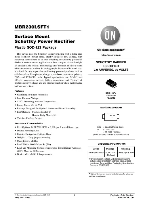
MBR230LSFT1Surface MountSchottky Power RectifierPlastic SOD-123 PackageThis device uses the Schottky Barrier principle with a large area metal-to-silicon power diode. I deally suited for low voltage, high frequency rectification or as free wheeling and polarity protection diodes in surface mount applications where compact size and weight are critical to the system. This package also provides an easy to work with alternative to leadless 34 package style. Because of its small size,it is ideal for use in portable and battery powered products such as cellular and cordless phones, chargers, notebook computers, printers,PDAs and PCMCI A cards. Typical applications are AC-DC and DC-DC converters, reverse battery protection, and “Oring” of multiple supply voltages and any other application where performance and size are critical.Features•ăGuardring for Stress Protection •ăLow Forward V oltage•ă125°C Operating Junction Temperature •ăEpoxy Meets UL 94 V-0•ăPackage Designed for Optimal Automated Board Assembly •ăESD Ratings:Machine Model, CHuman Body Model, 3B•ăThis is a Pb-Free DeviceMechanical Characteristics•ăReel Options: MBR230LSFT1 = 3,000 per 7 in reel/8 mm tapeā•ăDevice Marking: L3N•ăPolarity Designator: Cathode Band •ăWeight: 11.7 mg (approximately)•ăCase: Epoxy, Molded•ăLead Finish: 100% Matte Sn (Tin)•ăLead and Mounting Surface Temperature for Soldering Purposes:260°C Max. for 10 Seconds•ăDevice Meets MSL 1 RequirementsPreferred devices are recommended choices for future use and best overall value.DevicePackageShipping †ORDERING INFORMATION†For information on tape and reel specifications,including part orientation and tape sizes, please refer to our Tape and Reel Packaging Specification Brochure, BRD8011/D.MBR230LSFT1G SOD-123FL(Pb-Free)3000/Tape & ReelMAXIMUM RATINGSRating Symbol Value UnitPeak Repetitive Reverse Voltage Working Peak Reverse Voltage DC Blocking Voltage V RRMV RWMV R30VAverage Rectified Forward Current (At Rated V R, T L = 105°C)I O 2.0A Peak Repetitive Forward Current(At Rated V R, Square Wave, 100 kHz, T L = 95°C)I FRM 4.0ANon-Repetitive Peak Surge Current(Non-Repetitive peak surge current, halfwave, single phase, 60 Hz)I FSM40A Storage Temperature T stg-55 to 150°C Operating Junction Temperature T J-55 to 125°C Voltage Rate of Change (Rated V R, T J = 25°C)dv/dt10,000V/m s THERMAL CHARACTERISTICSThermal Resistance, Junction-to-Lead (Note 1) Thermal Resistance, Junction-to-Lead (Note 2) Thermal Resistance, Junction-to-Ambient (Note 1) Thermal Resistance, Junction-to-Ambient (Note 2)R tjlR tjlR tjaR tja262132582°C/WStresses exceeding Maximum Ratings may damage the device. Maximum Ratings are stress ratings only. Functional operation above the Recommended Operating Conditions is not implied. Extended exposure to stresses above the Recommended Operating Conditions may affect device reliability.1.Mounted with minimum recommended pad size, PC Board FR4.2.Mounted with 1 in. copper pad (Cu area 700 mm2).ELECTRICAL CHARACTERISTICSMaximum Instantaneous Forward Voltage (Note 3)V F T J = 25°C T J = 100°C V(I F = 1.0 A) (I F = 2.0 A)0.380.430.300.37Maximum Instantaneous Reverse Current (Note 3)I R T J = 25°C T J = 100°C mA (V R = 30 V) 1.0253.Pulse Test: Pulse Width ≤ 250 m s, Duty Cycle ≤2%.TYPICAL CHARACTERISTICSFigure 3. Typical Reverse Current Figure 4. Maximum Reverse Current1010.1I F , I N S T A N T A N E O U S F O R W A R D C U R R E N T (A M P S )V R , REVERSE VOLTAGE (VOLTS)I R , R E V E R S E C U R R E N T (A M P S )V R , REVERSE VOLTAGE (VOLTS)I R ,I O , A V E R A G E F O R W A R D C U R R E N T (A M P S )T L , LEAD TEMPERATURE (°C)Figure 5. Current Derating1.400.6P F O , A V E R A G E P O W E R D I S S I P A T I O N (W A T T S )0.20.41.20.81.0I O , AVERAGE FORWARD CURRENT (AMPS)1.6Figure 6. Forward Power DissipationTYPICAL CHARACTERISTICSFigure 7. CapacitanceFigure 8. Typical Operating TemperatureDeratingV R , REVERSE VOLTAGE (VOLTS)101000C , C A P A C I T A N C E (p F )V R , DC REVERSE VOLTAGE (VOLTS)1151059585756570125T J , D E R A T E D O P E R A T I N G T E M P E R A T U R E (°C )1001101009080120r (t ), T R A N S I E N T T H E R M A L R E S I S T A N C EFigure 9. Thermal Response10000.10.00001t 1, TIME (sec)0.00010.0010.011101000.0000010.1PACKAGE DIMENSIONSSOD-123LF CA SE 498-01ISSUE A*For additional information on our Pb-Free strategy and solderingdetails, please download the ON Semiconductor Soldering and Mounting Techniques Reference Manual, SOLDERRM/D.SOLDERING FOOTPRINT*cNOTES:1.DIMENSIONING AND TOLERANCING PER ANSI Y14.5M,1982.2.CONTROLLING DIMENSION: MILLIMETER.3.DIMENSIONS A AND B DO NOT INCLUDE MOLD FLASH.4.DIMENSIONS D AND J ARE TO BE MEASURED ON FLAT SECTION OF THE LEAD: BETWEEN 0.10 AND 0.25 MM FROM THE LEAD TIP.DIM A MIN NOM MAX MINMILLIMETERS0.900.95 1.000.035INCHES A10.000.050.100.000b 0.700.90 1.100.028c 0.100.150.200.004D 1.50 1.65 1.800.059E 2.50 2.70 2.900.098L 0.550.750.950.0220.0370.0390.0020.0040.0350.0430.0060.0080.0650.0710.1060.1140.0300.037NOM MAX 3.40 3.60 3.800.1340.1420.150H E --0°8°0°8°qǒmm inchesǓON Semiconductor and are registered trademarks of Semiconductor Components Industries, LLC (SCILLC). SCILLC reserves the right to make changes without further notice to any products herein. SCILLC makes no warranty, representation or guarantee regarding the suitability of its products for any particular purpose, nor does SCILLC assume any liability arising out of the application or use of any product or circuit, and specifically disclaims any and all liability, including without limitation special, consequential or incidental damages.“Typical” parameters which may be provided in SCILLC data sheets and/or specifications can and do vary in different applications and actual performance may vary over time. All operating parameters, including “Typicals” must be validated for each customer application by customer's technical experts. SCILLC does not convey any license under its patent rights nor the rights of others. SCILLC products are not designed, intended, or authorized for use as components in systems intended for surgical implant into the body, or other applications intended to support or sustain life, or for any other application in which the failure of the SCILLC product could create a situation where personal injury or death may occur. Should Buyer purchase or use SCILLC products for any such unintended or unauthorized application, Buyer shall indemnify and hold SCILLC and its officers, employees, subsidiaries, affiliates,and distributors harmless against all claims, costs, damages, and expenses, and reasonable attorney fees arising out of, directly or indirectly, any claim of personal injury or death associated with such unintended or unauthorized use, even if such claim alleges that SCILLC was negligent regarding the design or manufacture of the part. SCILLC is an Equal Opportunity/Affirmative Action Employer. This literature is subject to all applicable copyright laws and is not for resale in any manner.PUBLICATION ORDERING INFORMATION。