
页面提取自- 欧司朗-2
- 格式:pdf
- 大小:16.97 MB
- 文档页数:30
3.01
DULUX EL
3.07
3.08
3.08
3.09
3.10
3.11
3.12
3.13
3.14
3.15-3.16
3.17
3.18
3.19-3.20
3.21
COMPACT
?
Mini Twist
5
16W20W13%
l
d
E14
3.01
DULUX EL
3.07
3.08
3.08
3.09
3.10
3.11
3.12
3.13
3.14
3.15-3.16
3.17
3.18
3.19-3.20
3.21
COMPACT
?
Mini Twist
5
16W20W13%
l
d
E14

ARTICLEReceived1Apr2014|Accepted9Jan2015|Published24Feb2015Observation of long-lived interlayer excitonsin monolayer MoSe2–WSe2heterostructuresPasqual Rivera1,John R.Schaibley1,Aaron M.Jones1,Jason S.Ross2,Sanfeng Wu1,Grant Aivazian1,Philip Klement1,Kyle Seyler1,Genevieve Clark2,Nirmal J.Ghimire3,4,Jiaqiang Yan4,5,D.G.Mandrus3,4,5, Wang Yao6&Xiaodong Xu1,2Van der Waals bound heterostructures constructed with two-dimensional materials,such asgraphene,boron nitride and transition metal dichalcogenides,have sparked wide interest indevice physics and technologies at the two-dimensional limit.One highly coveted hetero-structure is that of differing monolayer transition metal dichalcogenides with type-II bandalignment,with bound electrons and holes localized in individual monolayers,that is,interlayer excitons.Here,we report the observation of interlayer excitons in monolayerMoSe2–WSe2heterostructures by photoluminescence and photoluminescence excitationspectroscopy.Wefind that their energy and luminescence intensity are highly tunable by anapplied vertical gate voltage.Moreover,we measure an interlayer exciton lifetime of B1.8ns,an order of magnitude longer than intralayer excitons in monolayers.Our work demonstratesoptical pumping of interlayer electric polarization,which may provoke further explorationof interlayer exciton condensation,as well as new applications in two-dimensional lasers,light-emitting diodes and photovoltaic devices.1Department of Physics,University of Washington,Seattle,Washington98195,USA.2Department of Materials Science and Engineering,University of Washington,Seattle,Washington98195,USA.3Department of Physics and Astronomy,University of T ennessee,Knoxville,T ennessee37996,USA.4Materials Science and T echnology Division,Oak Ridge National Laboratory,Oak Ridge,T ennessee37831,USA.5Department of Materials Science and Engineering,University of T ennessee,Knoxville,T ennessee37996,USA.6Department of Physics and Center of Theoretical and Computational Physics, University of Hong Kong,Hong Kong,China.Correspondence and requests for materials should be addressed to P.R.(email:pasqual@)or to X.X. (email:xuxd@).T he recently developed ability to vertically assemble different two-dimensional(2D)materials heralds a newrealm of device physics based on van der Waals heterostructures(HSs)1.The most successful example to date is the vertical integration of graphene on boron nitride.Such novel HSs not only markedly enhance graphene’s electronic properties2, but also give rise to superlattice structures demonstrating exotic physical phenomena3–5.A fascinating counterpart to gapless graphene is a class of monolayer direct bandgap semiconductors, namely transition metal dichalcogenides(TMDs)6–8.Due to the large binding energy in these2D semiconductors,excitons dominate the optical response,exhibiting strong light–matter interactions that are electrically tunable9,10.The discovery of excitonic valley physics11–15and strongly coupled spin and pseudospin physics16,17in2D TMDs opens up new possibilities for device concepts not possible in other material systems. Monolayer TMDs have the chemical formula MX2where the M is tungsten(W)or molybdenum(Mo),and the X is sulfur(S) or selenium(Se).Although these TMDs share the same crystalline structure,their physical properties,such as bandgap,exciton resonance and spin–orbit coupling strength,can vary signifi-cantly.Therefore,an intriguing possibility is to stack different TMD monolayers on top of one another to form2D HSs.First-principle calculations show that heterojunctions formed between monolayer tungsten and molybdenum dichalcogenides have type-II band alignment18–20.Recently,this has been confirmed by X-ray photoelectron spectroscopy and scanning tunnelling spectroscopy21.Since the Coulomb binding energy in2D TMDs is much stronger than in conventional semiconductors, it is possible to realize interlayer excitonic states in van der Waals bound heterobilayers,that is,bound electrons and holes that are localized in different layers.Such interlayer excitons have been intensely pursued in bilayer graphene for possible exciton condensation22,but direct optical observation demonstrating the existence of such excitons is challenging owing to the lack of a sizable bandgap in graphene.Monolayer TMDs with bandgaps in the visible range provide the opportunity to optically pump interlayer excitons,which can be directly observed through photoluminescence(PL)measurements.In this report,we present direct observation of interlayer excitons in vertically stacked monolayer MoSe2–WSe2HSs.We show that interlayer exciton PL is enhanced under optical excitation resonant with the intralayer excitons in isolated monolayers,consistent with the interlayer charge transfer resulting from the underlying type-II band structure.We demonstrate the tuning of the interlayer exciton energy by applying a vertical gate voltage,which is consistent with the permanent out-of-plane electric dipole nature of interlayer excitons.Moreover,wefind a blue shift in PL energy at increasing excitation power,a hallmark of repulsive dipole–dipole interac-tions between spatially indirect excitons.Finally,time-resolved PL measurements yield a lifetime of1.8ns,which is at least an order of magnitude longer than that of intralayer excitons.Our work shows that monolayer semiconducting HSs are a promising platform for exploring new optoelectronic phenomena.ResultsMoSe2–WSe2HS photoluminescence.HSs are prepared by standard polymethyl methacrylate(PMMA)transfer techniques using mechanically exfoliated monolayers of WSe2and MoSe2(see Methods).Since there is no effort made to match the crystal lattices of the two monolayers,the obtained HSs are considered incom-mensurate.An idealized depiction of the vertical MoSe2–WSe2HS is shown in Fig.1a.We have fabricated six devices that all show similar results as those reported below.The data presented here are from two independent MoSe2–WSe2HSs,labelled device1and device2.Figure1b shows an optical micrograph of device1,which has individual monolayers,as well as a large area of vertically stacked HS.This device architecture allows for the comparison of the excitonic spectrum of individual monolayers with that of the HS region,allowing for a controlled identification of spectral changes resulting from interlayer coupling.We characterize the MoSe2–WSe2monolayers and HS using PL measurements.Inspection of the PL from the HS at room temperature reveals three dominant spectral features(Fig.1c). The emission at1.65and1.57eV corresponds to the excitonic states from monolayer WSe2and MoSe2(refs10,15),respectively. PL from the HS region,outlined by the dashed white line in Fig.1a,reveals a distinct spectral feature at1.35eV(X I).Two-dimensional mapping of the spectrally integrated PL from X I shows that it is isolated entirely to the HS region(inset,Fig.1c), with highly uniform peak intensity and spectral position (Supplementary Materials1).Low-temperature characterization of the HS is performed with 1.88eV laser excitation at20K.PL from individual monolayer WSe2(top),MoSe2(bottom)and the HS area(middle)are shown with the same scale in Fig.1d.At low temperature,the intralayer neutral(X M o)and charged(X MÀ)excitons are resolved10,15,where M labels either W or parison of the three spectra shows that both intralayer X M o and X MÀexist in the HS with emission at the same energy as from isolated monolayers,demonstrating the preservation of intralayer excitons in the HS region.PL from X I becomes more pronounced and is comparable to the intralayer excitons at low temperature.We note that the X I energy position has variation across the pool of HS samples we have studied (Supplementary Fig.1),which we attribute to differences in the interlayer separation,possibly due to imperfect transfer and a different twisting angle between monolayers.We further perform PL excitation(PLE)spectroscopy to investigate the correlation between X I and intralayer excitons.A narrow bandwidth(o50kHz)frequency tunable laser is swept across the energy resonances of intralayer excitons(from1.6to 1.75eV)while monitoring X I PL response.Figure2a shows an intensity plot of X I emission as a function of photoexcitation energy from device2.We clearly observe the enhancement of X I emission when the excitation energy is resonant with intralayer exciton states(Fig.2b).Now we discuss the origin of X I.Since X I has never been observed in our exfoliated monolayer and bilayer samples,if its origin were related to defects,they must be introduced by the fabrication process.This would result in sample-dependent X I properties with non-uniform spatial dependence.However,our data show that key physical properties of X I,such as the resonance energy and intensity,are spatially uniform and isolated to the HS region(inset of Fig.1c and Supplementary Fig.2).In addition,X I has not been observed in WSe2–WSe2homo-structures constructed from exfoliated or physical vapor deposi-tion(PVD)grown monolayers(Supplementary Fig.3).All these facts suggest that X I is not a defect-related exciton.Instead,the experimental results support the observation of an interlayer exciton.Due to the type-II band alignment of the MoSe2–WSe2HS18–20,as shown in Fig.2c,photoexcited electrons and holes will relax(dashed lines)to the conduction band edge of MoSe2and the valence band edge of WSe2,respectively.The Coulomb attraction between electrons in the MoSe2and holes in the WSe2gives rise to an interlayer exciton,X I,analogous to spatially indirect excitons in coupled quantum wells.The interlayer coupling yields the lowest energy bright exciton in the HS,which is consistent with the temperature dependence of X I PL,that is,it increases as temperature decreases (Supplementary Fig.4).From the intralayer and interlayer exciton spectral positions,we can infer the band offsets between the WSe 2and MoSe 2monolayers (Fig.2c).The energy difference between X W and X I at room temperature is 310meV.Considering the smaller binding energy of interlayer than intralayer excitons,this sets a lower bound on the conduction band offset.The energy difference between X M and X I then provides a lower bound on the valence band offset of 230meV.This value is consistent with the valence band offset of 228meV found in MoS 2–WSe 2HSs by micro X-ray photoelectron spectroscopy and scanning tunnelling spectro-scopy measurements 21.This experimental evidence strongly corroborates X I as an interlayer exciton.The observation of bright interlayer excitons in monolayer semiconducting HSs is of central importance,and the remainder of this paper will focus on their physical properties resulting from their spatially indirect nature and the underlying type-II band alignment.WSe 2HSMoSe 2W M SeIn te n s i t y (a .u .)1.31.51.7Energy (eV)MoSe 2HeterostructureWSe 2W0WX X X X −0MoMo−e hehe h1.3 1.41.51.6 1.7I n t e n s i t y (a .u .)Energy (eV)5μm 0123×104Y (μm )246X (μm)0246Figure 1|Intralayer and interlayer excitons of a monolayer MoSe 2–WSe 2vertical heterostructure.(a )Cartoon depiction of a MoSe 2–WSe 2heterostructure (HS).(b )Microscope image of a MoSe 2–WSe 2HS (device 1)with a white dashed line outlining the HS region.(c )Room-temperature photoluminescence of the heterostructure under 20m W laser excitation at 2.33eV.Inset:spatial map of integrated PL intensity from the low-energy peak (1.273–1.400eV),which is only appreciable in the heterostructure area,outlined by the dashed black line.(d )Photoluminescence of individual monolayers and the HS at 20K under 20m W excitation at 1.88eV (plotted on the samescale).Energy (eV)WSe MoSe PL energy (eV)E x c i t a t i o n e n e r g y (e V )1.28 1.3 1.32 1.34 1.36 1.381.61.651.71.754,0006,0008,00010,000IntensityFigure 2|Photoluminescence excitation spectroscopy of the interlayer exciton at 20K.(a )PLE intensity plot of the heterostructure region with an excitation power of 30m W and 5s charge-coupled device CCD integration time.(b )Spectrally integrated PLE response (red dots)overlaid on PL (black line)with 100m W excitation at 1.88eV.(c )Type-II semiconductor band alignment diagram for the 2D MoSe 2–WSe 2heterojunction.interlayer exciton .Applying vertical energy of Figure 3a contact stacked insu-Electrostatic contact shows the 100to about analogue of reversed,varied expected for from reduces device 2,conduction 3b,c.of the in the on top band-offset at X I PL energy of basis of would should have X I PL This effect,intensity.further Power dependence and lifetime of interlayer exciton PL .The interlayer exciton PLE spectrum as a function of laser power with excitation energy in resonance with X W o reveals several properties of the X I .Inspection of the normalized PLE intensity (Fig.4a)shows the evolution of a doublet in the interlayer excitonspectrum,highlighted by the red and Both peaks of the doublet display a consistent increased laser intensity,shown by the dashed which are included as a guide to the eye.intensity of X I also exhibits a strong saturation laser power,as shown in Fig.4b (absolute Supplementary Fig.6).The sublinear power excitation powers above 0.5m W is distinctly the intralayer excitons in isolated monolayers,saturation power threshold of about Fig.7).The low power saturation of X I PL lifetime than that of intralayer excitons.the intralayer exciton is substantially reduced interlayer charge hopping 23,which is quenching of intralayer exciton PL (Fig.Fig.8).Moreover,the lifetime of the interlayer because it is the lowest energy configuration indirect nature leads to a reduced optical long lifetime is confirmed by time-resolved Fig.4c.A fit to a single exponential decay exciton lifetime of 1.8±0.3ns.This timescale the intralayer exciton lifetime,which is ps 24–27.By modelling the saturation behaviour three-level diagram,the calculated saturation interlayer exciton is about 180times (Supplementary Fig.7;Supplementary with our observation of low saturation intensity DiscussionWe attribute the observed doublet feature splitting of the monolayer MoSe 2conduction assignment is mainly based on the fact difference between the doublet is B 25with MoSe 2conduction band splitting predicted calculations 28.This explanation is also supported by the evolution of the relative strength of the two peaks with increasing excitation power,as shown in Fig.4a (similar results in device 1with 1.88eV excitation shown in Supplementary Fig.9).At low power,the lowest energy configuration of interlayer excitons,with the electron in the lower spin-split band of MoSe 2,is populated first.Due to phase space filling effects,the interlayer excitonSiO 2n + Si2MoSe 2e –h +e –h +P Ee –h +V g < 0WSe 2MoSe 2WSe 2MoSe 2h ωV g = 0Photon energy (eV)1.321.361.41.444080e –h +h +PL intensity (a.u.) -hω’-the interlayer exciton and band alignment.(a )Device 2geometry.The interlayer exciton has a out-of-plane electric polarization.(b )Electrostatic control of the band alignment and the interlayer exciton photoluminescence as a function of applied gate voltage under 70m W excitation at 1.744eV,1s integrationconfiguration with the electron in the higher energy spin-split band starts to be filled at higher laser power.Consequently,the higher energy peak of the doublet becomes more prominent at higher excitation powers.The observed blue shift of X I as the excitation power increases,indicated by the dashed arrows in Fig.4a,is a signature of the repulsive interaction between the dipole-aligned interlayer excitons (cf.Fig.3a).This is a hallmark of spatially indirect excitons in gallium arsenide (GaAs)coupled quantum wells,which have been intensely studied for exciton Bose-Einstein condensation (BEC)phenomena 29.The observation of spatially indirect interlayer excitons in a type-II semiconducting 2D HS provides an intriguing platform to explore exciton BEC,where the observed extended lifetimes and repulsive interactions are two key ingredients towards the realization of this exotic state of matter.Moreover,the extraordinarily high binding energy for excitons in this truly 2D system may provide for degenerate exciton gases at elevated temperatures compared with other material systems 30.The long-lived interlayer exciton may also lead to new optoelectronic applications,such as photovoltaics 31–34and 2D HS nanolasers.MethodsDevice fabrication .Monolayers of MoSe 2are mechanically exfoliated onto 300nm SiO 2on heavily doped Si wafers and monolayers of WSe 2onto a layer of PMMA atop polyvinyl alcohol on Si.Both monolayers are identified with an opticalmicroscope and confirmed by their PL spectra.Polyvinyl alcohol is dissolved in H 2O and the PMMA layer is then placed on a transfer loop or thin layer of poly-dimethylsiloxane (PDMS).The top monolayer is then placed in contact with the bottom monolayer with the aid of an optical microscope and micromanipulators.The substrate is then heated to cause the PMMA layer to release from the transfer media.The PMMA is subsequently dissolved in acetone for B 30min and then rinsed with isopropyl alcohol.Low-temperature PL measurements .Low-temperature measurements are con-ducted in a temperature-controlled Janis cold finger cryostat (sample in vacuum)with a diffraction-limited excitation beam diameter of B 1m m.PL is spectrally filtered through a 0.5-m monochromator (Andor–Shamrock)and detected on a charge-coupled device (Andor—Newton).Spatial PL mapping is performed using a Mad City Labs Nano-T555nanopositioning system.For PLE measurements,a continuous wave Ti:sapphire laser (MSquared—SolsTiS)is used for excitation and filtered from the PL signal using an 815-nm-long pass optical filter (Semrock).Electrostatic doping is accomplished with an indium drain contact deposited onto the monolayer WSe 2region of device 2and using the heavily doped Si as a tunable backgate.Time-resolved PL measurements .For interlayer lifetime measurements,we excite the sample with a o 200-fs pulsed Ti:sapphire laser (Coherent—MIRA).Interlayer PL is spectrally filtered through a 0.5-m monochromator (Princeton—Acton 2500),and detected with a fast time-correlated single-photon counting system composed of a fast (o 30ps full width at half maximum)single-photon avalanche detector (Micro Photon Devices—PDM series)and a picosecond event timer (PicoQuant—PicoHarp 300).References1.Geim,A.K.&Grigorieva,I.V.Van der Waals heterostructures.Nature 499,419–425(2013).2.Dean,C.R.et al.Boron nitride substrates for high-quality graphene electronics.Nat.Nanotechnol.5,722–726(2010).3.Hunt,B.et al.Massive Dirac fermions and Hofstadter butterfly in a van derWaals heterostructure.Science 340,1427–1430(2013).4.Dean,C.R.et al.Hofstadter’s butterfly and the fractal quantum Hall effect inmoire superlattices.Nature 497,598–602(2013).5.Ponomarenko,L.A.et al.Cloning of Dirac fermions in graphene superlattices.Nature 497,594–597(2013).6.Novoselov,K.S.et al.Two-dimensional atomic crystals.Proc.Natl Acad.SciUSA 102,10451–10453(2005).7.Mak,K.F.,Lee,C.,Hone,J.,Shan,J.&Heinz,T.F.Atomically thin MoS 2:anew direct-gap semiconductor.Phys.Rev.Lett.105,136805(2010).8.Splendiani,A.et al.Emerging photoluminescence in monolayer MoS 2.NanoLett.10,1271–1275(2010).MoSe2WSe 2dPhoton energy (eV)Laser power (μW)Time (ns)I n t e n s i t y (a .u .)N o r m a l i z e d P L E i n t e n s i t y (c o u n t s (μW s )–1)Power (μW)I n t e g r a t e d P L E i n t e n s i t y (C o u n t s (μW s )–1)2060404Figure 4|Power-dependent photoluminescence of interlayer exciton and its lifetime at 20K.(a )Power dependence of the interlayer exciton for 1.722eV excitation with a bi-Lorentzian fit to the 5and 100m W plots,normalized for power and charge-coupled device (CCD)integration time.(b )Spectrally integrated intensity of the interlayer exciton emission as a function of excitation power shows the saturation effect.(c )Time-resolvedphotoluminescence of the interlayer exciton (1.35eV)shows a lifetime of about 1.8ns.The dashed curve is the instrument response to the excitation laser pulse.(d )Illustration of the heterojunction band diagram,including the spin levels of the MoSe 2conduction band.The X I doublet has energy splitting equal to (o 0I Ào I )E 25meV.9.Mak,K.F.et al.Tightly bound trions in monolayer MoS2.Nat.Mater.12,207–211(2013).10.Ross,J.S.et al.Electrical control of neutral and charged excitons in amonolayer mun.4,1474(2013).11.Xiao,D.,Liu,G.-B.,Feng,W.,Xu,X.&Yao,W.Coupled spin and valleyphysics in monolayers of MoS2and other group-VI dichalcogenides.Phys.Rev.Lett.108,196802(2012).12.Cao,T.et al.Valley-selective circular dichroism of monolayer molybdenummun.3,887(2012).13.Zeng,H.,Dai,J.,Yao,W.,Xiao,D.&Cui,X.Valley polarization inMoS2monolayers by optical pumping.Nat.Nanotechnol.7,490–493(2012).14.Mak,K.F.,He,K.,Shan,J.&Heinz,T.F.Control of valley polarization inmonolayer MoS2by optical helicity.Nat.Nanotechnol.7,494–498(2012). 15.Jones,A.M.et al.Optical generation of excitonic valley coherence inmonolayer WSe2.Nat.Nanotechnol.8,634–638(2013).16.Gong,Z.et al.Magnetoelectric effects and valley-controlled spin quantumgates in transition metal dichalcogenide mun.4,2053(2013).17.Jones,A.M.et al.Spin-layer locking effects in optical orientation of excitonspin in bilayer WSe2.Nat.Phys.10,130–134(2014).18.Kang,J.,Tongay,S.,Zhou,J.,Li,J.&Wu,J.Band offsets and heterostructuresof two-dimensional semiconductors.Appl.Phys.Lett.102,012111–012114 (2013).19.Kos´mider,K.&Ferna´ndez-Rossier,J.Electronic properties of the MoS2-WS2heterojunction.Phys.Rev.B87,075451(2013).20.Terrones,H.,Lopez-Urias,F.&Terrones,M.Novel hetero-layered materialswith tunable direct band gaps by sandwiching different metal disulfides and diselenides.Sci.Rep.3,1549(2013).21.Chiu,M.-H.et al.Determination of band alignment in transition metaldichalcogenide heterojunctions,Preprint at http://arXiv:1406.5137(2014). 22.Su,J.-J.&MacDonald,A.H.How to make a bilayer exciton condensateflow.Nat.Phys.4,799–802(2008).23.Hong,X.P.et al.Ultrafast charge transfer in atomically thin MoS2/WS2heterostructures.Nat.Nanotechnol.9,682–686(2014).24.Wang,G.et al.Valley dynamics probed through charged and neutral excitonemission in monolayer WSe2.Phys.Rev.B90,075413(2014).garde,D.et al.Carrier and polarization dynamics in monolayer MoS2.Phys.Rev.Lett.112,047401(2014).26.Mai,C.et al.Many-body effects in valleytronics:direct measurement of valleylifetimes in single-layer MoS2.Nano Lett.14,202–206(2013).27.Shi,H.et al.Exciton dynamics in suspended monolayer and few-layer MoS22Dcrystals.ACS Nano7,1072–1080(2012).28.Korma´nyos,A.,Zo´lyomi,V.,Drummond,N.D.&Burkard,G.Spin-orbitcoupling,quantum dots,and qubits in monolayer transition metaldichalcogenides.Phys.Rev.X4,011034(2014).29.Butov,L.V.,Lai,C.W.,Ivanov,A.L.,Gossard,A.C.&Chemla,D.S.TowardsBose-Einstein condensation of excitons in potential traps.Nature417,47–52 (2002).30.Fogler,M.M.,Butov,L.V.&Novoselov,K.S.High-temperature superfluiditywith indirect excitons in van der Waals mun.5,4555 (2014).31.Lee,C.H.et al.Atomically thin p-n junctions with van der Waalsheterointerfaces.Nat.Nanotechnol.9,676–681(2014).32.Furchi,M.M.,Pospischil,A.,Libisch,F.,Burgdorfer,J.&Mueller,T.Photovoltaic effect in an electrically tunable van der Waals heterojunction.Nano Lett.14,4785–4791(2014).33.Cheng,R.et al.Electroluminescence and photocurrent generation fromatomically sharp WSe2/MoS2heterojunction p-n diodes.Nano Lett.14,5590–5597(2014).34.Fang,H.et al.Strong interlayer coupling in van der Waals heterostructuresbuilt from single-layer chalcogenides.Proc.Natl A111,6198–6202 (2014).AcknowledgementsThis work is mainly supported by the US DoE,BES,Materials Sciences and Engineering Division(DE-SC0008145).N.J.G.,J.Y.and D.G.M.are supported by US DoE,BES, Materials Sciences and Engineering Division.W.Y.is supported by the Research Grant Council of Hong Kong(HKU17305914P,HKU9/CRF/13G),and the Croucher Foun-dation under the Croucher Innovation Award.X.X.thanks the support of the Cottrell Scholar Award.P.R.thanks the UW GO-MAP program for their support.A.M.J.is partially supported by the NSF(DGE-0718124).J.S.R.is partially supported by the NSF (DGE-1256082).S.W.and G.C.are partially supported by the State of Washington through the UW Clean Energy Institute.Device fabrication was performed at the Washington Nanofabrication Facility and NSF-funded Nanotech User Facility. Author contributionsX.X.and P.R.conceived the experiments.P.R.and P.K.fabricated the devices,assisted by J.S.R.P.R.performed the measurements,assisted by J.R.S.,A.M.J.,J.S.R.,S.W.and G.A. P.R.and X.X.performed data analysis,with input from W.Y.N.J.G.,J.Y.and D.G.M. synthesized and characterized the bulk WSe2crystals.X.X.,P.R.,J.R.S.and W.Y.wrote the paper.All authors discussed the results.Additional informationSupplementary Information accompanies this paper at / naturecommunicationsCompetingfinancial interests:The authors declare no competingfinancial interests. Reprints and permission information is available online at / reprintsandpermissions/How to cite this article:Rivera,P.et al.Observation of long-lived interlayer excitons in monolayer MoSe2–mun.6:6242doi:10.1038/ncomms7242(2015).。
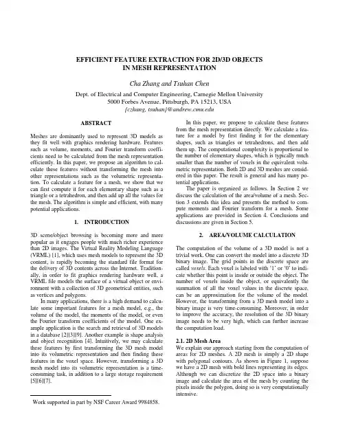
EFFICIENT FEATURE EXTRACTION FOR2D/3D OBJECTSIN MESH REPRESENTATIONCha Zhang and Tsuhan ChenDept.of Electrical and Computer Engineering,Carnegie Mellon University 5000Forbes Avenue,Pittsburgh,PA15213,USA{czhang,tsuhan}@ABSTRACTMeshes are dominantly used to represent3D models as they fit well with graphics rendering hardware.Features such as volume,moments,and Fourier transform coeffi-cients need to be calculated from the mesh representation efficiently.In this paper,we propose an algorithm to cal-culate these features without transforming the mesh into other representations such as the volumetric representa-tion.To calculate a feature for a mesh,we show that we can first compute it for each elementary shape such as a triangle or a tetrahedron,and then add up all the values for the mesh.The algorithm is simple and efficient,with many potential applications.1.INTRODUCTION3D scene/object browsing is becoming more and more popular as it engages people with much richer experience than2D images.The Virtual Reality Modeling Language (VRML)[1],which uses mesh models to represent the3D content,is rapidly becoming the standard file format for the delivery of3D contents across the Internet.Tradition-ally,in order to fit graphics rendering hardware well,a VRML file models the surface of a virtual object or envi-ronment with a collection of3D geometrical entities,such as vertices and polygons.In many applications,there is a high demand to calcu-late some important features for a mesh model,e.g.,the volume of the model,the moments of the model,or even the Fourier transform coefficients of the model.One ex-ample application is the search and retrieval of3D models in a database[2][3][9].Another example is shape analysis and object recognition[4].Intuitively,we may calculate these features by first transforming the3D mesh model into its volumetric representation and then finding these features in the voxel space.However,transforming a3D mesh model into its volumetric representation is a time-consuming task,in addition to a large storage requirement [5][6][7].Work supported in part by NSF Career Award9984858.In this paper,we propose to calculate these features from the mesh representation directly.We calculate a fea-ture for a model by first finding it for the elementary shapes,such as triangles or tetrahedrons,and then add them up.The computational complexity is proportional to the number of elementary shapes,which is typically much smaller than the number of voxels in the equivalent volu-metric representation.Both2D and3D meshes are consid-ered in this paper.The result is general and has many po-tential applications.The paper is organized as follows.In Section2we discuss the calculation of the area/volume of a mesh.Sec-tion3extends this idea and presents the method to com-pute moments and Fourier transform for a mesh.Some applications are provided in Section4.Conclusions and discussions are given in Section5.2.AREA/VOLUME CALCULATIONThe computation of the volume of a3D model is not a trivial work.One can convert the model into a discrete3D binary image.The grid points in the discrete space are called voxels.Each voxel is labeled with‘1’or‘0’to indi-cate whether this point is inside or outside the object.The number of voxels inside the object,or equivalently the summation of all the voxel values in the discrete space, can be an approximation for the volume of the model. However,the transforming from a3D mesh model into a binary image is very time-consuming.Moreover,in order to improve the accuracy,the resolution of the3D binary image needs to be very high,which can further increase the computation load.2.1.2D Mesh AreaWe explain our approach starting from the computation of areas for2D meshes.A2D mesh is simply a2D shape with polygonal contours.As shown in Figure1,suppose we have a2D mesh with bold lines representing its edges. Although we can discretize the2D space into a binary image and calculate the area of the mesh by counting the pixels inside the polygon,doing so is very computationally intensive."positive"area "negtive"areaFigure 1:The calculation of a 2D polygon area To start with our algorithm,let us make the assump-tion that the polygon is close.If it is not,a contour close process can be performed first [9].Since we know all the vertices and edges of the polygon,we can calculate the normal for each edge easily.For example,edge AB in Figure 1has the normal:2122121212)()(ˆ)(ˆ)(y y x x y x x xy y N AB −+−−+−−=(1)where (x 1,y 1)and (x 2,y 2)are the coordinates of vertices Aand B ,respectively,and xˆand y ˆare the unit vectors for the axes.We define the normal here as a normalized vec-tor which is perpendicular to the corresponding edge and pointing outwards of the mesh.In computer graphics lit-erature,there are different ways to check whether a point is inside or outside a polygon [8],thus it is easy to find the correct direction of the ter we will show that even if we only know that all the normals are pointing to the same side of the mesh (either inside or outside,as long as they are consistent),we are still able to find the correct area of the mesh.After getting the normals,we construct a set of trian-gles by connecting all the polygon vertices with the origin.Each edge and the origin form an elementary triangle,which is the smallest unit for computation.We define the signed area for each elementary triangle as below:The magnitude of this value is the area of the triangle,while the sign of the value is determined by checking the posi-tion of the origin with respect to the edge and the direction of the normal.Take the triangle OAB in Figure 1as an example.The area of OAB is:.)(212112y x y x S OAB +−=(2)The sign of S OAB is the same as the sign of the inner prod-uct AB N OA ⋅,which is positive in this case.The total area of the polygon can be computed by summing up all the signed areas .That is,¦=ii total S S (3)where i goes through all the edges or elementary triangles.Following the above steps,the result of equation (3)is guaranteed to be positive,no matter the origin is inside oroutside the mesh.Note here that we do not make any as-sumption that the polygon is convex.In real implementation,we do not need to check the signs of the areas each time.Let:().'',21'2112¦=+−=ii total i i i i i S S y x y x S (4)where i stands for the index of all the edges or elementary triangles.(x i1,y i1),(x i2,y i2)are coordinates of the starting point and the end point of edge i .When we loop through all the edges,we need to keep forwarding so that the in-side part of the mesh is always kept at the left hand side or the right hand side.According to the final sign of the result S’total ,we may know whether we are looping along the right direction (the right direction should give the positive result),and the final result can be simply achieved by tak-ing the magnitude of S’total .2.2.3D CaseWe can extend the above algorithm into the 3D case.In a VRML file,the mesh is represented by a set of vertices and polygons.Before we calculate the volume,we do some preprocessing on the model and make sure that all the polygons are triangles.Such preprocessing,called tri-angulation,is commonly used in mesh coding,mesh signal processing,and mesh editing.The direction of the normal for a triangle can be determined by the order of the verti-ces and the right-hand rule,as shown in Figure 2.The con-sistent condition is very easy to satisfy.For two neighbor-ing triangles,if the common edge has different directions,then the normals of the two triangles are consistent.For example,in Figure 2,AB is the common edge of triangle ACB and ABD .In triangle ACB ,the direction is from B to A ,and in triangle ABD ,the direction is from A toB ,thus N ACB and N ABD are consistent.BFigure 2:Normals and order of verticesIn the 3D case,the elementary calculation unit is a tet-rahedron.For each triangle,we connect each of its vertices with the origin and form a tetrahedron,as shown in Figure 3.As in the 2D case,we define the signed volume for each elementary tetrahedron as:The magnitude of its value is the volume of the tetrahedron,and the sign of the value is determined by checking if the origin is at the same side as the normal with respect to the triangle.In Figure 3,tri-2,z 2)Figure 3:The calculation of 3D volumeangle ACB has a normal N ACB .The volume of tetrahedron OACB is:.)(61321312231213132123z y x z y x z y x z y x z y x z y x V OACB +−−++−=(5)As the origin O is at the opposite side of N ACB ,the sign of this tetrahedron is positive.The sign can also be calculated by inner product ACB N OA ⋅.In real implementation,again we only need to com-pute:()¦=+−−++−=iitotal i i i i i i i i i i i i i i i i i i i V V z y x z y x z y x z y x z y x z y x V ''.61'321312231213132123(6)where i stands for the index of triangles or elementary tetrahedrons.(x i1,y i1,z i1),(x i2,y i2,z i2)and (x i3,y i3,z i3)are coordinates of the vertices of triangle i and they are or-dered so that the normal of triangle i is consistent with others.Volume of a 3D mesh model is always positive.The final result can be achieved by take the absolute value of V’total .In order to compute other 3D model features such as moments or Fourier transform coefficients,we reverse the sequence of vertices for each triangle if V’total turns out to be negative.3.MOMENTS AND FOURIER TRANSFORMThe above algorithm can be generalized to calculate other features for 2D and 3D mesh models.Actually,whenever the feature to be calculated can be written as a signed sum of features of the elementary shape (triangle in the 2D case and tetrahedron in the 3D case),and the feature of the elementary shape can be derived in an explicit form,the proposed algorithm applies.Although this seems to be a strong constrain,many of the commonly-used fea-tures fall into this category.For example,all the features that have the form of integration over the space inside the object can be calculated with this algorithm.This includes moments,Fourier transform,wavelet transform,and many others.In classical mechanics and statistical theory,the con-cept of moments is used extensively.In this paper,themoments of a 3D mesh model are defined as:³³³=dxdydzz y x z y x M r q p pqr ),,(ρ(7)where ),,(z y x ρis an indicator function:¯®=otherwise.,0meshthe inside is z)y,(x,if ,1),,(z y x ρ(8)and p ,q ,r are the orders of the moment.Central moments can be obtained easily from the result of equation (7).Since the integration can be rewritten as the sum of inte-grations over each elementary shape:¦³³³=ii r q p i pqr dxdydz z y x z y x s M ),,(ρ(9)where ),,(z y x i ρis the indicator function for elementary shape i ,and s i is the sign of the signed volume for shape i .We can use the same process as that in Section 2to calculate a number of low order moments for triangles and tetrahedrons that are extensively used.A few examples for the moments of a tetrahedron are given in the Appendix.More examples can be found in [9].Fourier transform is a very powerful tool in many sig-nal processing applications.The Fourier transform of a 2D or 3D mesh model is defined by the Fourier transform of its indicator function:³³³++−=Θdxdydzz y x e w v u zw yv xu i ),,(),,()(ρ(10)Since Fourier transform is also an integration over the space inside the object,it can also be calculated by de-composing the integration into integrations over each ele-mentary shape.The explicit form of the Fourier transform of a tetrahedron is given in the Appendix.As the moments and Fourier transform coefficients of an elementary shape are explicit,the above computation is very efficient.The computational complexity is O (N),where N is the number of edges or triangles in the mesh.Note that in the volumetric approach,where a 2D or 3D binary image is obtained first before getting any of the features,the computational complexity is O (M),where M is the number of grid points inside the model,not consid-ering the cost of transforming the data representation.It is obvious that M is typically much larger that N ,especially when a relatively accurate result is required and the resolu-tion of the binary image has to be large.The storage space required by our algorithm is also much smaller.Previous work by Lien and Kajiya [10]provide a similar method for calculating the moments for tetrahe-drons.Our work gives more explicit forms of the moments and extends their work to calculating the Fourier trans-form.4.APPLICATIONSA good application of our algorithm is to find the principal axes of a 3D mesh model.This is useful when we want to compare two 3D models that are not well aligned.In a 3Dmodel retrieval system [2][9],this is required because some of the features may not be invariant to arbitrary rota-tions.We construct a 3x3matrix by the second order mo-ments of the 3D model:.002011101011020110101110200»»»¼º«««¬ª=M M M M M M M M M S (11)The principal axes are obtained by computing the ei-genvectors of matrix S ,which is also known as the princi-ple component analysis (PCA).The eigenvector corre-sponding to the largest eigenvalue is made the first princi-pal axis.The next eigenvector corresponding to the secon-dary eigenvalue is the second principal axis,and so on.Inorder to make the final result unique,we further make sure that the 3rd order moments,M 300and M 030,are positive after the transform.Figure 4shows the results of this algo-rithm.Before rotationAfter rotationBefore rotation After rotationFigure 4:3D models before and after PCAThe Fourier transform of a 3D mesh model can be used in many applications.For example,the coefficients can be directly used as features in a retrieval system [9].Other applications are shape analysis,object recognition,and model matching.Note that in our algorithm,the result-ing Fourier transform is in continuous form.There is no discretization alias since we can evaluate a Fourier trans-form coefficient from the continuous form directly.5.CONCLUSIONS AND DISCUSSIONSIn this paper,we propose an algorithm for computing fea-tures for a 2D or 3D mesh model.Explicit methods to compute the volume,moments and Fourier transform from a mesh representation directly are given.The algorithm is very efficient,and has many potential applications.The proposed algorithm still has some room for im-provement.For example,it is still difficult to get the ex-plicit form of a high order moment for a triangles and tet-rahedrons.Also the Fourier transform may lose its compu-tational efficiency if many coefficients are required simul-taneously.More research is in progress to speed this up.REFERENCES[1]R.Carey,G.Bell,and C.Marrin,“The Virtual Reality Modeling Language”.Apr.1997,ISO/IEC DIS 14772-1.[Online]:/Specifications/.[2]Eric Paquet and Marc Rioux,“A Content-based Search Engine for VRML Database”,Computer Vision and Pattern Recognition,1998.Proceedings.1998,IEEE Computer Society Conference on ,pp.541-546,1998.[3]Sylvie Jeannin,Leszek Cieplinski,Jens Rainer Ohm,Munchurl Kim,MPEG-7Visual part of eXperimentation Model Version 7.0,ISO/IEC JTC1/SC29/WG11/N3521,Beijing,July 2000.[4]Anthony P.Reeves,R.J.Prokop,Susan E.Andrews and Frank P.Kuhl,“Three-Dimensional Shape Analysis Using Moments and Fourier Descriptors”,IEEE Trans.Pattern Analysis and Machine Intelligence ,pp.937-943,Vol.10,No.6,Nov.1988.[5]Homer H.Chen,Thomas S.Huang,“A Survey of Construction and Manipulation of Octrees”,Computer Vision,Graphics,and Image Processing ,pp.409-431,Vol.43,1988.[6]Shi-Nine Yang and Tsong-Wuu Lin,“A New Linear Octree Con-struction by Filling Algorithms”,Computers and Communications,1991.Conference Proceedings.Tenth Annual International Phoenix Conference on ,pp.740-746,1991.[7]Yoshifumi Kitamura and Fumio Kishino,“A Parallel Algorithm for Octree Generation from Polyhedral Shape Representation”,Pattern Recognition,1996.Proceedings of the 13th International Conference on ,pp.303-309,Vol.3,1996.[8]James D.Foley,Andries van Dam,Steven K.Feiner,and John F.Hughes,Computer Graphics principles and practice,Second Edition ,Addison-Wesley Publishing Company,Inc.,1996.[9]/projects/3DModelRetrieval/.[10]Sheue-ling Lien and James T.Kajiya,“A Symbolic Method for Calculating the Integral Properties of Arbitrary Nonconvex Polyhedra”,IEEE Computer Graphics and Applications ,pp.35-41,Oct.1984.APPENDIX().61321312231213132123000z y x z y x z y x z y x z y x z y x M +−−++−=().00032110041M x x x M ++=().000313221232221200101M x x x x x x x x x M +++++=()000321212331223221333231300x x x )()()(201M x x x x x x x x x x x x M +++++++++=))()((i))()((e *i ))()((e *i ))()((e *i (*),,(333222111323232313131333)wz vy i(ux 323232212121222)wz vy i(ux 313131212121111)wz vy i(ux 000333222111wz vy ux wz vy ux wz vy ux wz wz vy vy ux ux wz wz vy vy ux ux wz vy ux wz wz vy vy ux ux wz wz vy vy ux ux wz vy ux wz wz vy vy ux ux wz wz vy vy ux ux wz vy ux M w v u ++++++−+−+−+−+−+−+−+++−+−+−+−+−+−+++−+−+−−+−+−++=ℑ++++++。

Walldim202多功能触摸式玻璃面板控制器概述Walldim202是欧切斯设计的高端多功能触摸式玻璃面板控制器系列的产品之一,它具有界面时尚美观,功能齐全,简单易用,按键触摸灵敏等特点。
它主要应用于连接LED 0-10V 调光控制器或电源,可以根据不同的需求实现0-10V的平滑调光。
产品特点●12V-15VDC供电●输出两通道0-10V 模拟调光信号●可同时调节灯具的亮度和色温●LED亮度条显示当前亮度或色温等级●可安装在DIN 49073和国内标准86电气盒●界面时尚美观,简单易用技术参数外观尺寸(mm)功能描述(1)开关:短按,打开或关闭面板输出,关闭面板输出时,指示灯输出最低亮度;长按5s以上打开或关闭按键音,(2)指示灯:显示当前亮度或色温等级,(3)亮度+/亮度-:调节LED灯具亮度,长按可以快速调节(4)色温+/色温-:调节LED灯具色温,长按可以快速调节注:若10s内没有对面板进行操作,指示灯将进入低亮状态;再次操作时亮度恢复接口描述◆电源输入接口直流 12-15V 输入,为面板供电◆信号输出接口两路0-10V模拟信号输出,分别控制两组0-10V 调光控制器或调光电源应用接线图安装说明1. 在墙体上安装电气盒2. 如图所示用螺丝刀沿着后盖下方缺口的缝隙轻轻的撬开后盖3. 将输出线和电源线依次连接在玻璃面板背面上相应的输入输出端4. 如图所示,用螺钉将后盖嵌入电气盒内,以确保安装牢固5. 将玻璃面板卡住后盖备注:1.先连接灯具线,再连接电源线,请确保在打开电源前连接线之间不会发生短路。
2.输入电压直流12-15V,超过这个电压值可能会烧掉控制器。
