
GTL-OS-70072中文资料
- 格式:pdf
- 大小:168.81 KB
- 文档页数:2


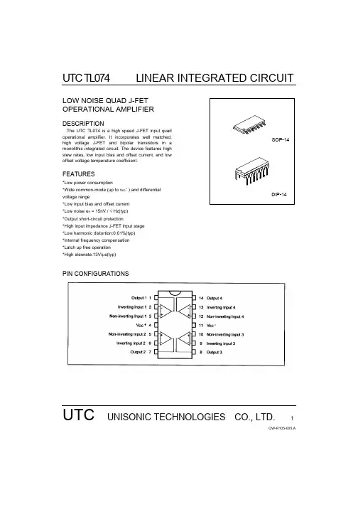
UTC TL074LINEAR INTEGRATED CIRCUITUTC UNISONIC TECHNOLOGIES CO., LTD.1QW-R105-005,ALOW NOISE QUAD J-FET OPERATIONAL AMPLIFIERDESCRIPTIONThe UTC TL074 is a high speed J-FET input quad operational amplifier. It incorporates well matched,high voltage J-FET and bipolar transistors in a monolithic integrated circuit. The device features high slew rates, low input bias and offset current, and low offset voltage temperature coefficient.FEATURES*Low power consumption*Wide common-mode (up to v cc + ) and differential voltage range*Low input bias and offset current *Low noise e n = 15nV / √ Hz(typ)*Output short-circuit protection*High input impedance J-FET input stage *Low harmonic distortion:0.01%(typ)*Internal frequency compensation *Latch up free operation *High slewrate:13V/µs(typ)PIN CONFIGURATIONSUTC TL074LINEAR INTEGRATED CIRCUITUTC UNISONIC TECHNOLOGIES CO., LTD.2QW-R105-005,ASCHEMATIC DIAGRAMABSOLUTE MAXIMUM RATINGS (Ta=25°C )PARAMETERSYMBOLVALUEUNIT Supply Voltage (note 1)Vcc +-18V Input Voltage (note 2)Vi +-15V Differential Input Voltage (note 3)Vid +-30V Power DissipationPtot 680mW Output Short-Circuit Duration (Note 4)Infinite Operating Free Air Temperature Toper 0 to 70°C Storage TemperatureTstg5 to 150°CNOTES: 1. All voltage values, except differential voltage, are with respect to the zero reference level (ground) ofthe supply voltages where the zero reference level is the midpoint between Vcc- and Vcc+.2. The magnitude of the input voltage must never exceed the magnitude of the supply voltage or 15 volts,whichever is less.3. Differential voltages are at the non-inverting input terminal with respect to the inverting input terminal.4. The output may be shorted to ground or to either supply. Temperature and/or supply voltages must be limited to ensure that the dissipation rating is not exceeded.UTC TL074LINEAR INTEGRATED CIRCUITUTC UNISONIC TECHNOLOGIES CO., LTD.3QW-R105-005,AUTC TL074C ELECTRICAL CHARACTERISTICS ( Vcc=+-15V, Ta=25°C , unless otherwisespecified)PARAMETER SYMBOLMIN TYP MAX UNIT Input Offset Voltage(Rs=50Ω), Ta=25°C Tmin<=Ta<=TmaxVio31013mVTemperature Coefficient of Input Offset VoltageDvio 10¦ÌV /¡æInput Offset Current*Ta=25°CTmin<=Ta<=TmaxIio510010pA nA Input Bias Current*Ta=25°CTmin<=Ta<=TmaxIib3020020pA nA Input Common Mode Voltage Vicm +-11-12~+15VOutput Voltage Swing(R L =10k Ω)Ta=25°C, R L =2k Ω,Ta=25°C, R L =10k ΩTmin<=Ta<=Tmax, R L =2k ΩTmin<=Ta<=Tmax, R L =10k ΩVopp 101210121213.5V Large Signal Voltage Gain(R L =2k Ω, Vo=+-10V) Ta=25°CTmin<=Ta<=TmaxAvd 2515200V/mV Gain Bandwidth Product(Ta=25°C, R L =10k Ω,f=100kHz, Vin=10mV, C L =100pF)GBP 23MHz Input Resistance Ri 1012ΩCommon Mode Rejection Ratio(R S =50Ω)Ta=25°CTmin<=Ta<=TmaxCMR 707086dB Supply Voltage Rejection Ratio(R S =50Ω)Ta=25°CTmin<=Ta<=TmaxSVR 707086dB Supply Current( no load)Ta=25°CTmin<=Ta<=TmaxIcc 1. 4 2. 52.5mAChannel Separation(Av=100, Ta=25°C)V 01/V 02120dB Output Short-circuit Current Ta=25°CTmin<=Ta<=TmaxIos 1010406060mASlew Rate(Vi=10V, R L =2k Ω, C L =100pF,Ta=25°C, unity gain)SR 813V/µsRise Time(Vi=20mV, R L =2k Ω, C L =100pF,Ta=25°C, unity gain)t r 0.1µsOvershoot Factor(Vi=20mV, R L =2k Ω,C L =100pF, Ta=25°C, unity gain)Kov 10%Total Harmonic Distortion(Av=20dB, f=1kHz R L =2k Ω, C L =100pF, Ta=25Ω, Vo=2Vpp)THD 0.01%Phase Margin 45DegreesEquivalent Input Noise Voltage(R S =100Ω,f=1KHz)e n 15*The Input bias currents are junction leakage currents, which approximately double for every 10°C increase in the junction temperature.UTC TL074LINEAR INTEGRATED CIRCUITUTC UNISONIC TECHNOLOGIES CO., LTD.4QW-R105-005,AUTC TL074AC ELECTRICAL CHARACTERISTICS ( Vcc=+-15V, Ta=25°C , unless otherwisespecified)PARAMETER SYMBOLMIN TYP MAX UNIT Input Offset Voltage(Rs=50Ω), Ta=25°C Tmin<=Ta<=TmaxVio367mVTemperature Coefficient of Input Offset Voltage(Rs=50Ω)Dvio 10µV/°C Input Offset Current*Ta=25°CTmin<=Ta<=TmaxIio51004pA nA Input Bias Current*Ta=25°CTmin<=Ta<=TmaxIib2020020pA nA Input Common Mode Voltage Vicm +-11-12~+15VOutput Voltage Swing(R L =10k Ω)Ta=25°C, R L =2k Ω,Ta=25°C, R L =10k ΩTmin<=Ta<=Tmax, R L =2k ΩTmin<=Ta<=Tmax, R L =10k ΩVopp 101210121213.5V Large Signal Voltage Gain(R L =10k Ω, Vo=+-10V) Ta=25°CTmin<=Ta<=TmaxAvd 5025200V/mV Gain Bandwidth Product(Ta=25°C, R L =10k Ω,C L =100pF)GBP 23MHz Input Resistance Ri 1012ΩCommon Mode Rejection Ratio(R S =50Ω)Ta=25°CTmin<=Ta<=TmaxCMR 808086dB Supply Voltage Rejection Ratio(R S =50Ω)Ta=25°CTmin<=Ta<=TmaxSVR 808086dB Supply Current( no load)Ta=25°CTmin<=Ta<=TmaxIcc 1. 4 2. 52.5mAChannel Separation(Av=100, Ta=25°C)V 01/V 02120dB Output Short-circuit Current Ta=25°CTmin<=Ta<=TmaxIos 1010406060mASlew Rate(Vi=10V, R L =2k Ω, C L =100pF,Ta=25°C, unity gain)SR 813V/µsRise Time(Vi=20mV, R L =2k Ω, C L =100pF,Ta=25°C, unity gain)t r 0.1µsOvershoot Factor(Vi=20mV, R L =2k Ω,C L =100pF, Ta=25°C, unity gain)Kov 10%Total Harmonic Distortion(Av=20dB, f=1kHz R L =2k Ω, C L =100pF, Ta=25°C, Vo=2Vpp)THD 0.01%Phase Margin 45DegreesEquivalent Input Noise Voltage(R S =100Ω,f=1KHz)e n 15*The Input bias currents are junction leakage currents, which approximately double for every 10°C increase in the junction temperature.UTC TL074LINEAR INTEGRATED CIRCUITUTC UNISONIC TECHNOLOGIES CO., LTD.5QW-R105-005,AUTC TL074BC ELECTRICAL CHARACTERISTICS ( Vcc=+-15V, Ta=25°C , unless otherwisespecified)PARAMETER SYMBOLMIN TYP MAX UNIT Input Offset Voltage(Rs=50Ω), Ta=25°C Tmin<=Ta<=TmaxVio135mVTemperature Coefficient of Input Offset Voltage(Rs=50Ω)Dvio 10¦ÌV /¡æInput Offset Current*Ta=25°CTmin<=Ta<=TmaxIio51004pA nA Input Bias Current*Ta=25°CTmin<=Ta<=TmaxIib2020020pA nA Input Common Mode Voltage Vicm +-11-12~+15VOutput Voltage Swing(R L =10k Ω)Ta=25°C, R L =2k Ω,Ta=25°C, R L =10k ΩTmin<=Ta<=Tmax, R L =2k ΩTmin<=Ta<=Tmax, R L =10k ΩVopp 101210121213.5V Large Signal Voltage Gain(R L =10k Ω, Vo=+-10V) Ta=25°CTmin<=Ta<=TmaxAvd 5025200V/mV Gain Bandwidth Product(Ta=25°C, R L =10k Ω,C L =100pF)GBP 23MHz Input Resistance Ri 1012ΩCommon Mode Rejection Ratio(R S =50Ω)Ta=25°CTmin<=Ta<=TmaxCMR 808086dB Supply Voltage Rejection Ratio(R S =50Ω)Ta=25°CTmin<=Ta<=TmaxSVR 808086dB Supply Current( no load)Ta=25°CTmin<=Ta<=TmaxIcc 1. 4 2. 52.5mAChannel Separation(Av=100, Ta=25°C)V 01/V 02120dB Output Short-circuit Current Ta=25°CTmin<=Ta<=TmaxIos 1010406060mASlew Rate(Vi=10V, R L =2k Ω, C L =100pF,Ta=25°C, unity gain)SR 813V/µsRise Time(Vi=20mV, R L =2k Ω, C L =100pF,Ta=25°C, unity gain)t r 0.1µsOvershoot Factor(Vi=20mV, R L =2k Ω,C L =100pF, Ta=25°C, unity gain)Kov 10%Total Harmonic Distortion(Av=20dB, f=1kHz R L =2k Ω, C L =100pF, Ta=25°C, Vo=2Vpp)THD 0.01%Phase Margin 45DegreesEquivalent Input Noise Voltage(R S =100Ω,f=1KHz)e n 15*The Input bias currents are junction leakage currents, which approximately double for every 10°C increase in the junction temperature.UTC TL074LINEAR INTEGRATED CIRCUITUTC UNISONIC TECHNOLOGIES CO., LTD.6QW-R105-005,AUTC TL074LINEAR INTEGRATED CIRCUITUTC UNISONIC TECHNOLOGIES CO., LTD.7QW-R105-005,AUTC TL074LINEAR INTEGRATED CIRCUITUTC UNISONIC TECHNOLOGIES CO., LTD.8QW-R105-005,AUTC TL074LINEAR INTEGRATED CIRCUITUTC UNISONIC TECHNOLOGIES CO., LTD.9QW-R105-005,APARAMETER MEASUREMENT INFORMATIONTYPICAL APPLICATIONS。

DMG80480F070_01WTR产品概述:●基于T5L0芯片,运行DGUS II系统。
●7寸,800*480分辨率,262K色,TN屏,普通视角。
●液晶屏与触摸屏框贴工艺,产品厚度仅5.1mm。
●COF结构,将智能屏的整个核心电路固定于液晶模组FPC上,适合结构要求轻、薄,成本要求苛刻,生产简单的应用。
●排线共50个pin脚,引出用户CPU核的IO、UART、CAN、AD、PWM等接口,二次开发十分方便。
Features:●Based on T5L0,running DGUS II system.●7inch,800*480pixels resolution,262K colors,TN-TFT-LCD,normal viewing angel.●LCD and TP frame lamination process,only5.1mm thickness.●COF structure.The entire core circuit of the smart screen is fixed on the FPC of LCM,featured by lightand thin structure,low cost and easy production.●50pins,including IO,UART,CAN,AD and PWM from user CPU core for easy secondary development.1外部接口External InterfacePIN 序号Definition 定义I/O Functional Description 功能描述1+5V I 供电输入,DC3.6-5.5V 。
Power supply,DC3.6-5.5V.2+5V I 3GND GND GND4GND GND 5GND GND 6AD7I 5路ADC 输入,3.3V 电源做为参考,12bit 分辨率,输入电压范围0-3.3V 。

Microprocessor Reset ICFeaturesPrecision Monitoring of +3V, +3.3V, and +5V Power-Supply VoltagesFully Specified Over TemperatureAvailable in Three Output Configurations Push-Pull RESET Output (G670L)Push-Pull RESET Output (G670H)Open-Drain RESET Output (G671L)2ms max Power-On Reset Pulse Width14µA Supply CurrentGuaranteed Reset Valid to V CC = +1VPower Supply Transient ImmunityNo External Components3-Pin SOT-23,TO-92 and SOT-89 Packages 2% Threshold AccuracyApplicationsComputersControllersIntelligent InstrumentsCritical µP and µC Power MonitoringPortable / Battery-Powered EquipmentAutomotive General DescriptionThe G670/G671 are microprocessor (µP) supervisory circuits used to monitor the power supplies in µP and digital systems. They provide excellent circuit reliability and low cost by eliminating external components and adjustments when used with +5V, +3.3V, +3.0V- pow-ered circuits.These circuits perform a single function: they assert a reset signal whenever the V CC supply voltage declines below a preset threshold. Reset thresholds suitable for operation with a variety of supply voltages are avail-able.The G671L has an open-drain output stage, while the G670 have push-pull outputs. The G671L’s open-drain RESET output requires a pull-up resistor that can be connected to a voltage higher than V CC. The G670L have an active-low RESET output, while the G670H has an active-high RESET output. The reset com-parator is designed to ignore fast transients on V CC, and the outputs are guaranteed to be in the correct logic state for V CC down to 1V.Low supply current makes the G670/G671 ideal for use in portable equipment. The G670/G671 are avail-able in 3-pin SOT-23, TO-92 and SOT-89 packages.Pin Configuration Typical Application CircuitTopVCC*G671 only SOT-2312123SOT-89TO-92132ViewOrdering InformationORDER NUMBER ORDER NUMBER(Pb free)TEMP. RANGE OUTPUT TYPEG670LxxxTDxB G670LxxxTDxBf -40°C ~ +105°C Push-Pull Active LowG670HxxxTDxB G670HxxxTDxBf -40°C ~ +105°C Push-Pull Active HighG671LxxxTDxB G671LxxxTDxBf -40°C ~ +105°C Open-Drain G670LxxxT2xU G670LxxxT2xUf -40°C ~ +105°C Push-Pull Active LowG670HxxxT2xU G670HxxxT2xUf -40°C ~ +105°C Push-Pull Active HighG671LxxxT2xU G671LxxxT2xUf -40°C ~ +105°C Open-Drain G670LxxxT7xU G670LxxxT7xUf -40°C ~ +105°C Push-Pull Active LowG670HxxxT7xU G670HxxxT7xUf -40°C ~ +105°C Push-Pull Active HighG671LxxxT7xU G671LxxxT7xUf -40°C ~ +105°C Open-Drain Note: U : Tape & Reel B: BagOrder Number IdentificationPin OptionTypeThreshold Voltage OptionPart NumberPART NUMBER THRESHOLD VOLTAGE OPTIONG670L : Push-Pull Active Low Output * xxx specifies the threshold voltage.G670H : Push-Pull Active High Output e.g. 263 denotes the 2.64V threshold voltage.G671L : Open-Drain OutputPACKAGE TYPE PIN OPTIONTD : TO-92 1 2 3T2 : SOT-89 1 :RESET GND V CCT7 : SOT-23 2 :RESET V CC GND3 : GND RESET V CC4 : GND V CC RESET5 : V CC GND RESET6 : V CC RESET GND*RESET for G670HSelector GuideTOP MARK ORDER NUMBERORDER NUMBER(Pb free)RESETTHRESHOLD (V)OUTPUT TYPETO-92G671L463TD5B G671L463TD5Bf 4.60Open-Drain663G xx G671L438TD5B G671L438TD5Bf 4.32 Open-Drain663Fxx G671L400TD5B G671L400TD5Bf 3.96 Open-Drain663Exx G671L330TD5B G671L330TD5Bf 3.30 Open-Drain663Dxx G671L308TD5B G671L308TD5Bf 3.10 Open-Drain663Cxx G671L293TD5B G671L293TD5Bf 2.91 Open-Drain663Bxx G671L263TD5B G671L263TD5Bf 2.64 Open-Drain663Axx G670H463TD5B G670H463TD5Bf 4.60 Push-Pull RESET662Nxx G670H438TD5B G670H438TD5Bf 4.32 Push-Pull RESET662Mxx G670H400TD5B G670H400TD5Bf 3.96 Push-Pull RESET662Lxx G670H330TD5B G670H330TD5Bf 3.30 Push-Pull RESET662Kxx G670H308TD5B G670H308TD5Bf 3.10 Push-Pull RESET662Jxx G670H293TD5B G670H293TD5Bf 2.91 Push-Pull RESET662Ixx G670H263TD5B G670H263TD5Bf 2.64 Push-Pull RESET662Hxx G670L463TD5B G670L463TD5Bf 4.60 Push-Pull662Gxx G670L438TD5B G670L438TD5Bf 4.32 Push-Pull662Fxx G670L400TD5B G670L400TD5Bf 3.96 Push-Pull662Exx G670L330TD5B G670L330TD5Bf 3.30 Push-Pull662Dxx G670L308TD5B G670L308TD5Bf 3.10 Push-Pull662Cxx G670L293TD5B G670L293TD5Bf 2.91 Push-Pull662Bxx G670L263TD5B G670L263TD5Bf 2.64 Push-Pull662Axx Note: TD: TO-92Not all product options are ready for mass production, please contact factory for availability.Selector GuideTOP MARKORDER NUMBERORDER NUMBER(Pb free)RESETTHRESHOLD (V)OUTPUT TYPESOT-89G671L463T25U G671L463T25Uf 4.60 Open-Drain 663G xx G671L438T25U G671L438T25Uf 4.32 Open-Drain 663F xx G671L400T25U G671L400T25Uf 3.96 Open-Drain 663E xx G671L330T25U G671L330T25Uf 3.30 Open-Drain 663D xx G671L308T25U G671L308T25Uf 3.10 Open-Drain 663C xx G671L293T25U G671L293T25Uf 2.91 Open-Drain 663B xx G671L263T25U G671L263T25Uf 2.64 Open-Drain 663A xx G670H463T25U G670H463T25Uf 4.60 Push-Pull RESET 662N xx G670H438T25U G670H438T25Uf 4.32 Push-Pull RESET 662M xx G670H400T25U G670H400T25Uf 3.96 Push-Pull RESET 662L xx G670H330T25U G670H330T25Uf 3.30 Push-Pull RESET 662K xx G670H308T25U G670H308T25Uf 3.10 Push-Pull RESET 662J xx G670H293T25U G670H293T25Uf 2.91 Push-Pull RESET 662I xx G670H263T25U G670H263T25Uf 2.64 Push-Pull RESET662H xx G670L463T25U G670L463T25Uf 4.60 Push-Pull 662G xx G670L438T25U G670L438T25Uf 4.32 Push-Pull 662F xx G670L400T25U G670L400T25Uf 3.96 Push-Pull 662E xx G670L330T25U G670L330T25Uf 3.30 Push-Pull 662D xx G670L308T25U G670L308T25Uf 3.10 Push-Pull 662C xx G670L293T25U G670L293T25Uf 2.91 Push-Pull 662B xx G670L263T25U G670L263T25Uf2.64Push-Pull662A xxNote: T2: SOT-89Not all product options are ready for mass production, please contact factory for availability.Selector GuideTOP MARKORDER NUMBERORDER NUMBER(Pb free)RESETTHRESHOLD (V)OUTPUT TYPESOT-23G671L463T71U G671L463T71Uf 4.60 Open-Drain 669Gx G671L438T71U G671L438T71Uf 4.32 Open-Drain 669Fx G671L400T71U G671L400T71Uf 3.96 Open-Drain 669Ex G671L330T71U G671L330T71Uf 3.30 Open-Drain 669Dx G671L308T71U G671L308T71Uf 3.10 Open-Drain 669Cx G671L293T71U G671L293T71Uf 2.91 Open-Drain 669Bx G671L263T71U G671L263T71Uf 2.64 Open-Drain 669Ax G670H463T71U G670H463T71Uf 4.60 Push-Pull RESET 668Nx G670H438T71U G670H438T71Uf 4.32 Push-Pull RESET 668Mx G670H400T71U G670H400T71Uf 3.96 Push-Pull RESET 668Lx G670H330T71U G670H330T71Uf 3.30 Push-Pull RESET 668Kx G670H308T71U G670H308T71Uf 3.10 Push-Pull RESET 668Jx G670H293T71U G670H293T71Uf 2.91 Push-Pull RESET 668Ix G670H263T71U G670H263T71Uf 2.64 Push-Pull RESET668Hx G670L463T71U G670L463T71Uf 4.60 Push-Pull 668Gx G670L438T71U G670L438T71Uf 4.32 Push-Pull 668Fx G670L400T71U G670L400T71Uf 3.96 Push-Pull 668Ex G670L330T71U G670L330T71Uf 3.30 Push-Pull 668Dx G670L308T71U G670L308T71Uf 3.10 Push-Pull 668Cx G670L293T71U G670L293T71Uf 2.91 Push-Pull 668Bx G670L263T71U G670L263T71Uf2.64Push-Pull668AxNote: T7: SOT-23Not all product options are ready for mass production, please contact factory for availability.Selector GuideTOP MARKORDER NUMBERORDER NUMBER(Pb free)RESETTHRESHOLD (V)OUTPUT TYPESOT-23G671L463T72U G671L463T72Uf 4.60 Open-Drain 667Gx G671L438T72U G671L438T72Uf 4.32 Open-Drain 667Fx G671L400T72U G671L400T72Uf 3.96 Open-Drain 667Ex G671L330T72U G671L330T72Uf 3.30 Open-Drain 667Dx G671L308T72U G671L308T72Uf 3.10 Open-Drain 667Cx G671L293T72U G671L293T72Uf 2.91 Open-Drain 667Bx G671L263T72U G671L263T72Uf 2.64 Open-Drain 667Ax G670H463T72U G670H463T72Uf 4.60 Push-Pull RESET 666Nx G670H438T72U G670H438T72Uf 4.32 Push-Pull RESET 666Mx G670H400T72U G670H400T72Uf 3.96 Push-Pull RESET 666Lx G670H330T72U G670H330T72Uf 3.30 Push-Pull RESET 666Kx G670H308T72U G670H308T72Uf 3.10 Push-Pull RESET 666Jx G670H293T72U G670H293T72Uf 2.91 Push-Pull RESET 666Ix G670H263T72U G670H263T72Uf 2.64 Push-Pull RESET666Hx G670L463T72U G670L463T72Uf 4.60 Push-Pull 666Gx G670L438T72U G670L438T72Uf 4.32 Push-Pull 666Fx G670L400T72U G670L400T72Uf 3.96 Push-Pull 666Ex G670L330T72U G670L330T72Uf 3.30 Push-Pull 666Dx G670L308T72U G670L308T72Uf 3.10 Push-Pull 666Cx G670L293T72U G670L293T72Uf 2.91 Push-Pull 666Bx G670L263T72U G670L263T72Uf2.64Push-Pull666AxNote: T7: SOT-23Not all product options are ready for mass production, please contact factory for availability.Selector GuideTOP MARKORDER NUMBERORDER NUMBER(Pb free)RESETTHRESHOLD (V)OUTPUT TYPESOT-23G671L463T73U G671L463T73Uf 4.60 Open-Drain 671Gx G671L438T73U G671L438T73Uf 4.32 Open-Drain 671Fx G671L400T73U G671L400T73Uf 3.96 Open-Drain 671Ex G671L330T73U G671L330T73Uf 3.30 Open-Drain 671Dx G671L308T73U G671L308T73Uf 3.10 Open-Drain 671Cx G671L293T73U G671L293T73Uf 2.91 Open-Drain 671Bx G671L263T73U G671L263T73Uf 2.64 Open-Drain 671Ax G670H463T73U G670H463T73Uf 4.60 Push-Pull RESET 670Nx G670H438T73U G670H438T73Uf 4.32 Push-Pull RESET 670Mx G670H400T73U G670H400T73Uf 3.96 Push-Pull RESET 670Lx G670H330T73U G670H330T73Uf 3.30 Push-Pull RESET 670Kx G670H308T73U G670H308T73Uf 3.10 Push-Pull RESET 670Jx G670H293T73U G670H293T73Uf 2.91 Push-Pull RESET 670Ix G670H263T73U G670H263T73Uf 2.64 Push-Pull RESET670Hx G670L463T73U G670L463T73Uf 4.60 Push-Pull 670Gx G670L438T73U G670L438T73Uf 4.32 Push-Pull 670Fx G670L400T73U G670L400T73Uf 3.96 Push-Pull 670Ex G670L330T73U G670L330T73Uf 3.30 Push-Pull 670Dx G670L308T73U G670L308T73Uf 3.10 Push-Pull 670Cx G670L293T73U G670L293T73Uf 2.91 Push-Pull 670Bx G670L263T73U G670L263T73Uf2.64Push-Pull670AxNote: T7: SOT-23Not all product options are ready for mass production, please contact factory for availability.Selector GuideTOP MARKORDER NUMBERORDER NUMBER(Pb free)RESETTHRESHOLD (V)OUTPUT TYPESOT-23G671L463T76U G671L463T76Uf 4.60 Open-Drain 665Gx G671L438T76U G671L438T76Uf 4.32 Open-Drain 665Fx G671L400T76U G671L400T76Uf 3.96 Open-Drain 665Ex G671L330T76U G671L330T76Uf 3.30 Open-Drain 665Dx G671L308T76U G671L308T76Uf 3.10 Open-Drain 665Cx G671L293T76U G671L293T76Uf 2.91 Open-Drain 665Bx G671L263T76U G671L263T76Uf 2.64 Open-Drain 665Ax G670H463T76U G670H463T76Uf 4.60 Push-Pull RESET 664Nx G670H438T76U G670H438T76Uf 4.32 Push-Pull RESET 664Mx G670H400T76U G670H400T76Uf 3.96 Push-Pull RESET 664Lx G670H330T76U G670H330T76Uf 3.30 Push-Pull RESET 664Kx G670H308T76U G670H308T76Uf 3.10 Push-Pull RESET 664Jx G670H293T76U G670H293T76Uf 2.91 Push-Pull RESET 664Ix G670H263T76U G670H263T76Uf 2.64 Push-Pull RESET664Hx G670L463T76U G670L463T76Uf 4.60 Push-Pull 664Gx G670L438T76U G670L438T76Uf 4.32 Push-Pull 664Fx G670L400T76U G670L400T76Uf 3.96 Push-Pull 664Ex G670L330T76U G670L330T76Uf 3.30 Push-Pull 664Dx G670L308T76U G670L308T76Uf 3.10 Push-Pull 664Cx G670L293T76U G670L293T76Uf 2.91 Push-Pull 664Bx G670L263T76U G670L263T76Uf2.64Push-Pull664AxNote: T7: SOT-23Not all product options are ready for mass production, please contact factory for availability.Absolute Maximum RatingsTerminal Voltage (with respect to GND)V CC. . . . . . . . . . . . . . . . . . . . . . . . . . . . . .-0.3V to +6.0V RESET,RESET(push-pull) . . . . . -0.3V to (V CC + 0.3V) RESET(open drain) . . . . . . . . . . . . . . . .-0.3V to +6.0V Input Current, V CC. . . . . . . . . . . . . . . . . . . . . . . . ..20mA Output Current, RESET, RESET. . . . . . . . . . . . .20mA Continuous Power Dissipation (T A = +70°C)SOT-23 (derate 4mW/°C above +70°C) . . . .. . 100mW SOT-89 (derate 4mW/°C above +70°C). . . .. . .100mW TO-92 (derate 4mW/°C above +70°C). . . .. . . . 100mW Operating Temperature Range. . . .. . .-40°C to +105°C Storage Temperature Range. . . .. . . ..-65°C to +150°C Reflow Temperature (soldering, 10sec) . . . .. . .+260°CStresses beyond those listed under “Absolute Maximum Ratings” may cause permanent damage to the device. These are stress ratings only, and functional operation of the device at these or any other conditions beyond those indicated in the operational sections of the specifications is not implied. Exposure to absolute maximum rating conditions for extended periods may affect device reliability.Electrical Characteristics(V CC = full range, T A = -40°C to +105°C, unless otherwise noted. Typical values are at T A = +25°C, V CC = 5V for 463/438/400/330 versions, V CC= 3.3V for 308/293 versions, and V CC = 3V for 263 version.) (Note 1)ANote 2:RESET output is for G670L/G671L; While RESET output is for G670H.Typical Operating Characteristics(V CC = full range, T A = -40°C to +105°C, unless otherwise noted. Typical values are at T A = +25°C, V CC = 5V for 463/438/400 versions, V CC = 3.3V for 308/293 versions, and V CC = 3V for 263 version.)Recommended Minimum FootprintSOT-89SOT-23Detailed DescriptionA microprocessor’s (µP’s) reset input starts the µP in a known state. The G671L/G670L/G670H assert reset to prevent code-execution errors during power-up, power-down, or brownout conditions. They assert a reset signal whenever the V CC supply voltage declines below a preset threshold, keeping it asserted for at most 2ms after V CC has risen above the reset thresh-old. The G671L uses an open-drain output, and the G670L/G670H have a push-pull output stage. Connect a pull-up resistor on the G671L’s RESET output to any supply between 0 and 5.5V.Figure 1. Maximum Transient Duration Without Causing a Reset Pulse vs. Reset Com-parator OverdriveFigure 2. RESET Valid to V CC = Ground Circuit Applications InformationNegative-Going V CC TransientsIn addition to issuing a reset to the µP during power-up, power-down, and brownout conditions, the G671L/ G670H/G670L are relatively immune to short- duration negative-going V CC transients (glitches).Figure 1 shows typical transient duration vs. reset comparator overdrive, for which the G671L/G670H/ G670L do not generate a reset pulse. The graph was generated using a negative-going pulse applied to V CC, starting 0.5V above the actual reset threshold and ending below it by the magnitude indicated (reset comparator overdrive). The graph indicates the maxi-mum pulse width a negative-going V CC transient can have without causing a reset pulse. As the magnitude of the transient increases (goes farther below the reset threshold), the maximum allowable pulse width de-creases. Typically, for the G67_ _463 and G67_ _438, a V CC transient that goes 100mV below the reset threshold and lasts 7µs or less will not cause a reset pulse. A 0.1µF bypass capacitor mounted as close as possible to the V CC pin provides additional transient immunity.Ensuring a Valid Reset Output Down to V CC = 0 When V CC falls below 1V, the G670 RESET output no longer sinks current—it becomes an open circuit. Therefore, high-impedance CMOS logic inputs con-nected to RESET can drift to undetermined voltages. This presents no problem in most applications since most µP and other circuitry is inoperative with VCC below 1V. However, in applications where RESET must be valid down to 0V, adding a pull-down resistor to RESET causes any stray leakage currents to flow to ground, holding RESET low (Figure 2). R1’s value is not critical; 100kΩ is large enough not to load RESET and small enough to pull RESET to ground.A 100kΩ pull-up resistor to VCC is also recommended for the G671L if RESET is required to remain valid for V CC< 1V.Figure 3. Interfacing to µPs with Bidirectional Re-set I/OFigure 4. G671L Open-Drain RESET Output Allows Use with Multiple Supplies Interfacing to µPs with Bidirectional Reset Pins Since the RESET output on the G671L is open drain, this device interfaces easily with µPs that have bidirec-tional reset pins, such as the Motorola 68HC11. Con-necting the µP supervisor’s RESET output directly to the microcontroller’s (µC’s) RESET pin with a single pull-up resistor allows either device to assert reset (Figure 3).G671L Open-Drain RESET Output Allows Use with Multiple SuppliesGenerally, the pull-up connected to the G671L will connect to the supply voltage that is being monitored at the IC’s V CC pin. However, some systems may use the open-drain output to level-shift from the monitored supply to reset circuitry powered by some other supply (Figure 4). Note that as the G671L’s V CC decreases below 1V, so does the IC’s ability to sink current at RESET. Also, with any pull-up, RESET will be pulled high as VCC decays toward 0. The voltage where this occurs depends on the pull-up resistor value and the voltage to which it is connected.Benefits of Highly Accurate Reset ThresholdMost µP supervisor ICs have reset threshold voltages between 5% and 10% below the value of nominal supply voltages. This ensures a reset will not occur within 5% of the nominal supply, but will occur when the supply is 10% below nominal.When using ICs rated at only the nominal supply ±5%, this leaves a zone of uncertainty where the supply is between 5% and 10% low, and where the reset may or may not be asserted.The G67_ _463/G67_ _308 use highly accurate circuitry to ensure that reset is asserted close to the 5% limit, and long before the supply has declined to 10% below nominal.VPackage InformationTO-92 (TD) PackageMILLIMETER INCH SYMBOLMIN MAX MIN MAXA 3.35 3.86 0.132 0.152 A1 1.0414 1.55 0.041 0.061 b 0.254 0.508 0.010 0.020 E 4.34 4.85 0.1710.191 C 0.254 0.508 0.010 0.020 L 14.53 15.04 0.572 0.592 e 1.143 1.397 0.045 0.055 G 3.683 4.191 0.145 0.165 D 4.29 4.80 0.169 0.189 D1 4.34 4.85 0.171 0.191SOT-89 (T2) PackageDIMENSIONS IN MILLIMETER DIMENSIONS IN INCH SYMBOLMIN NOM MAX MIN NOM MAXA 1.40 1.50 1.60 0.055 0.059 0.063 A1 0.80 1.04 ----- 0.031 0.041 -----b 0.36 0.42 0.48 0.014 0.016 0.018 b1 0.41 0.47 0.53 0.016 0.0180.020 C 038 0.40 0.43 0.014 0.015 0.017 D 4.40 4.50 4.60 0.173 0.177 0.181 D1 1.40 1.60 1.75 0.055 0.062 0.069 HE ----- ----- 4.25 ----- ----- 0.167 E 2.40 2.50 2.60 0.094 0.098 0.102 e 2.90 3.00 3.10 0.114 0.118 0.122Package InformationSOT-23 (T7) PackageNote:1.Package body sizes exclude mold flash protrusions or gate burrs2.Tolerance ±0.1000 mm (4mil) unless otherwise specified3.Coplanarity: 0.1000mm4.Dimension L is measured in gage planeDIMENSIONS IN MILLIMETERSYMBOLMIN NOM MAXA 1.00 1.10 1.30A1 0.00 ----- 0.10A2 0.70 0.80 0.90 b 0.35 0.40 0.50C 0.10 0.15 0.25D 2.70 2.90 3.10E 1.40 1.60 1.80e ----- 1.90(TYP) ----- H 2.60 2.803.00L 0.37 ------ ----- θ1 1° 5° 9°Taping SpecificationPACKAGE Q ’TY/REEL Q ’TY/BY BAGTO-92 ----- 2,000 ea SOT-89 1,000 ea ----- SOT-23 3,000 ea -----GMT Inc. does not assume any responsibility for use of any circuitry described, no circuit patent licenses are implied and GMT Inc. reserves the right at any time without notice to change said circuitry and specifications.θ1A1SOT-89 Package OrientationSOT-23 Package Orientation。