
18244M
- 格式:pdf
- 大小:339.24 KB
- 文档页数:1
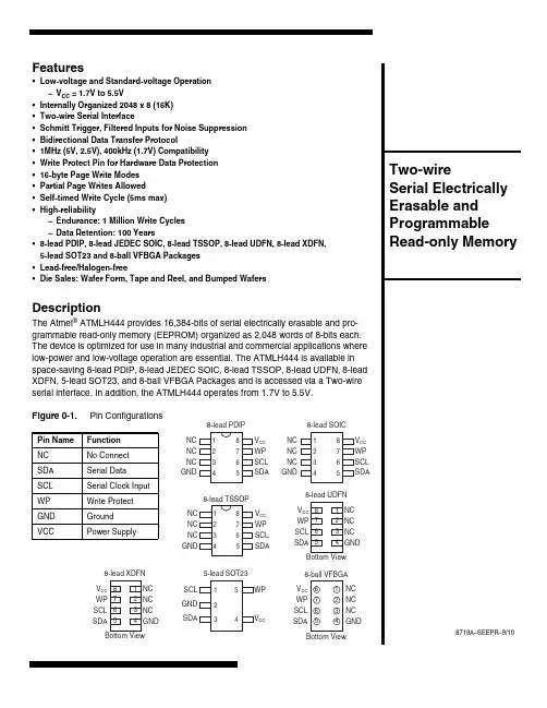
V CC WP SCL SDANC NC NC GND432156788-lead UDFNBottom ViewNC NC NC GND123487658-lead PDIPV CC WP SCL SDANC NC NC GND123487658-lead SOICV CC WP SCL SDA8-lead TSSOP 12348765NC NC NC GNDV CC WP SCL SDAV CC WP SCL SDANC NC NC GND123487658-ball VFBGABottom ViewV CC WP SCL SDANC NC NC GND432156788-lead XDFN Bottom View 12354SCL GND SDAWPV CC5-lead SOT23Features•Low-voltage and Standard-voltage Operation –V CC =1.7V to 5.5V•Internally Organized 2048x 8(16K)•Two-wire Serial Interface•Schmitt Trigger,Filtered Inputs for Noise Suppression •Bidirectional Data Transfer Protocol•1MHz (5V,2.5V),400kHz (1.7V)Compatibility •Write Protect Pin for Hardware Data Protection •16-byte Page Write Modes •Partial Page Writes Allowed•Self-timed Write Cycle (5ms max)•High-reliability–Endurance:1Million Write Cycles –Data Retention:100Years•8-lead PDIP,8-lead JEDEC SOIC,8-lead TSSOP,8-lead UDFN,8-lead XDFN,5-lead SOT23and 8-ball VFBGA Packages •Lead-free/Halogen-free•Die Sales:Wafer Form,Tape and Reel,and Bumped WafersDescriptionThe Atmel ®ATMLH444provides 16,384-bits of serial electrically erasable and pro-grammable read-only memory (EEPROM)organized as 2,048words of8-bits each.The device is optimized for use in many industrial and commercialapplications where low-power and low-voltage operation are essential.The ATMLH444is available in space-saving 8-lead PDIP,8-lead JEDEC SOIC,8-lead TSSOP,8-lead UDFN,8-lead XDFN,5-lead SOT23,and 8-ball VFBGA Packages and is accessed via a Two-wire serial interface.In addition,the ATMLH444operates from 1.7V to 5.5V.Figure 0-1.Pin ConfigurationsAbsolute Maximum RatingsFigure 0-2.Block Diagram*NOTICE:Stresses beyond those listed under “Absolute Maximum Ratings”may cause permanent damage to the device.This is a stress rating only and functional operation of the device at these or any other conditions beyond those indicated in the operational sections of this specification is not implied.Exposure to abso-lute maximum rating conditions for extended periods may affect device reliability.VCC GND WP SCL SDA1.Pin DescriptionSERIAL CLOCK(SCL):The SCL input is used to positive edge clock data into each EEPROM device andnegative edge clock data out of each device.SERIAL DATA(SDA):The SDA pin is bidirectional for serial data transfer.This pin is open-drain driven and may be wire-ORed with any number of other open-drain or open-collector devices.DEVICE/PAGE ADDRESSES:The Atmel®ATMLH444does not use the device address pins,which limits the number of devices on a single bus to one.WRITE PROTECT(WP):The ATMLH444has a write protect pin that provides hardware data protection.The write protect pin allows normal read/write operations when connected to ground(GND).When the write protect pin is connected to V CC,the write protection feature is enabled and operates as shown in<blue>Table1-1.Table1-1.Write Protect2.Memory OrganizationAtmel ATMLH444,16K SERIAL EEPROM:Internally organized with 128pages of 16-bytes each,the 16K requires an 11-bit data word address for random word addressing.Table 2-1.Pin Capacitance (1)Note:1.This parameter is characterized and is not 100%testedTable 2-2.DC CharacteristicsNote:1.V IL min and V IH max are reference only and are not testedApplicable over recommended operating range from T A =25⋅C,f =1.0MHz,V CC =+1.7VApplicable over recommended operating range from:T AI =−40⋅C to +85⋅C,V CC=+1.7V to +5.5V (unless otherwise noted)Table2-3.AC Characteristics(Industrial Temperature)Applicable over recommended operating range from T AI=−40⋅C to+85⋅C,V CC=+1.7V to+5.5V,CL=100pF (unless otherwise noted).Test conditions are listed in Note2.Notes: 1.This parameter is characterized and is not100%tested2.AC measurement conditions:R L(connects to V CC):1.3kΩ(2.5V,5.0V),10kΩ(1.7V)Input pulse voltages:0.3V CC to0.7V CCInput rise and fall times:≤50nsInput and output timing reference voltages:0.5V CC3.Device OperationCLOCK and DATA TRANSITIONS:The SDA pin is normally pulled high with an external device.Data on the SDA pin may change only during SCL low time periods(see<blue>Figure3-4on page7).Data changes during SCL high periods will indicate a start or stop condition as defined below.START CONDITION:A high-to-low transition of SDA with SCL high is a start condition which must precede any other command(see<blue>Figure3-5on page8).STOP CONDITION:A low-to-high transition of SDA with SCL high is a stop condition.After a read sequence,the stop command will place the EEPROM in a standby power mode(see<blue>Figure3-5on page8).ACKNOWLEDGE:All addresses and data words are serially transmitted to and from the EEPROM in8-bit words.The EEPROM sends a zero to acknowledge that it has received each word.This happens during the ninth clock cycle.STANDBY MODE:The Atmel®ATMLH444features a low-power standby mode which is enabled:(a)upon power-up and(b)after the receipt of the STOP bit and the completion of any internal operations.2-WIRE SOFTWARE RESET:After an interruption in protocol,power loss or system reset,any2-wire part can be protocol reset by following these steps:1.Create a start bit condition2.Clock nine cycles3.Create another start bit followed by stop bit condition as shown belowFigure3-1.Software ResetSCLSDAFigure 3-2.Bus TimingSCL:Serial Clock,SDA:Serial Data I/O ®Figure 3-3.Write Cycle TimingSCL:Serial Clock,SDA:Serial Data I/ONote:The write cycle time t WR is the time from a valid stop condition of a write sequence to the end of the internal clear/write cycleFigure 3-4.DataValiditySCLSDA INSDA OUTSCLSDASTOP CONDITIONSTART CONDITIONSDASCLDA T A ST ABLE DA TA STABLEDATA CHANGEFigure 3-5.Start and Stop DefinitionFigure 3-6.Output AcknowledgeSDASCLSTART STOPSCLDA T A INDA T A OUTSTART ACKNOWLEDGE9814.Device AddressingThe16K EEPROM device requires an8-bit device address word following a start condition to enable the chip for a read or write operation(refer to<blue>Figure6-1).The device address word consists of a mandatory one,zero sequence for the first four most significant bits as shown.This is common to all the EEPROM devices.The next three bits used for memory page addressing and are the most significant bits of the data word address which follows.The eighth bit of the device address is the read/write operation select bit.A read operation is initiated if this bit is high and a write operation is initiated if this bit is low.Upon a compare of the device address,the EEPROM will output a zero.If a compare is not made,the chip will return to a standby state.5.Write OperationsBYTE WRITE:A write operation requires an8-bit data word address following the device address word andacknowledgment.Upon receipt of this address,the EEPROM will again respond with a zero and then clock in the first8-bit data word.Following receipt of the8-bit data word,the EEPROM will output a zero and the addressing device,such as a microcontroller,must terminate the write sequence with a stop condition.At this time theEEPROM enters an internally timed write cycle,t WR,to the nonvolatile memory.All inputs are disabled during this write cycle and the EEPROM will not respond until the write is complete(see<blue>Figure6-2on page10).PAGE WRITE:The16K EEPROM is capable of an16-byte page write.A page write is initiated the same as a byte write,but the microcontroller does not send a stop condition after thefirst data word is clocked in.Instead,after the EEPROM acknowledges receipt of the first data word,themicrocontroller can transmit up to fifteen data words.The EEPROM will respond with a zero after each data word received.The microcontroller must terminate the page write sequence with a stop condition(see<blue>Figure6-3 on page11).The data word address lower four bits are internally incremented following the receipt of each data word.Thehigher data word address bits are not incremented,retaining the memory page row location.When the wordaddress,internally generated,reaches the page boundary,the following byte is placed at the beginning of thesame page.If more than sixteen data words are transmitted to the EEPROM,the data word address will“roll over”and previous data will be overwritten.ACKNOWLEDGE POLLING:Once the internally timed write cycle has started and the EEPROM inputs aredisabled,acknowledge polling can be initiated.This involves sending a start condition followed by the deviceaddress word.The read/write bit is representative of the operation desired.Only if the internal write cycle hascompleted will the EEPROM respond with a zero allowing the read or write sequence to continue.6.Read OperationsRead operations are initiated the same way as write operations with the exception that the read/write select bit in the device address word is set to one.There are three read operations:current address read,random address read and sequential read.CURRENT ADDRESS READ:The internal data word address counter maintains the last address accessed during the last read or write operation,incremented by one.This address stays valid between operations as long as the chip power is maintained.The address “roll over”during read is from the last byte of the last memory page to the first byte of the first page.The address “roll over”during write is from the last byte of the current page to the first byte of the same page.Once the device address with the read/write select bit set to one is clocked in and acknowledged by the EEPROM,the current address data word is serially clocked out.The microcontroller does not respond with an input zero but does generate a following stop condition (see <blue>Figure 6-4on page 11).RANDOM READ:A random read requires a “dummy”byte write sequence to load in the data word address.Once the device address word and data word address are clocked in and acknowledged by the EEPROM,themicrocontroller must generate another start condition.The microcontroller now initiates a current address read by sending a device address with the read/write select bit high.The EEPROM acknowledges the device address and serially clocks out the data word.The microcontroller does not respond with a zero but does generate a following stop condition (see <blue>Figure 6-5on page 11).SEQUENTIAL READ:Sequential reads are initiated by either a current address read or a random address read.After the microcontroller receives a data word,it responds with an acknowledge.As long as the EEPROM receives an acknowledge,it will continue to increment the data word address and serially clock out sequential data words.When the memory address limit is reached,the data word address will “roll over”and the sequential read will continue.The sequential read operation is terminated when the microcontroller does not respond with a zero but does generate a following stop condition (see <blue>Figure 6-6on page 11).Figure 6-1.Device AddressFigure 6-2.Byte WriteMSBLSB1 0 1 0 P2 P 1 P 0 R/W16K ST A R TW R I T ES T O PDEVICE ADDRESSWORD ADDRESS DATASDA LINEM S B A C K R /A C K A C KFigure 6-3.Page WriteFigure 6-4.Current Address ReadFigure 6-5.Random ReadFigure 6-6.Sequential ReadSDA LINES T A R TW R I TE DEVICE ADDRESSWORD ADDRESS (n)DATA (n)DATA (n + 1)DATA (n + x)M S B A C K R /W A C K A C K A C K A C KS T OPSDA LINES T A R TDEVICE ADDRESSR E A D S T O PM S B A C KR /W N O A C KDATASDA LINES T A R TS T A R TW R I T EDEVICE ADDRESS DEVICE ADDRESSWORD ADDRESS n R E A D S T O PM S BA C K R /W N O A C KDATA nDUMMY WRITEA C KA CKSDA LINEDEVICE ADDRESSR E A DA C K A C K A C KS T O PA C KR /W N O A C KDATA n DATA n + 1DATA n + 2DATA n + x8S1–JEDEC SOIC。

PACKAGING INFORMATIONOrderable Device Status(1)PackageType PackageDrawingPins PackageQtyEco Plan(2)Lead/Ball Finish MSL Peak Temp(3)SN74LV244ADBLE OBSOLETE SSOP DB20TBD Call TI Call TISN74LV244ADBR ACTIVE SSOP DB202000Green(RoHS&no Sb/Br)CU NIPDAU Level-1-260C-UNLIMSN74LV244ADBRE4ACTIVE SSOP DB202000Green(RoHS&no Sb/Br)CU NIPDAU Level-1-260C-UNLIMSN74LV244ADGVR ACTIVE TVSOP DGV202000Green(RoHS&no Sb/Br)CU NIPDAU Level-1-260C-UNLIMSN74LV244ADGVRE4ACTIVE TVSOP DGV202000Green(RoHS&no Sb/Br)CU NIPDAU Level-1-260C-UNLIMSN74LV244ADW ACTIVE SOIC DW2025Green(RoHS&no Sb/Br)CU NIPDAU Level-1-260C-UNLIMSN74LV244ADWE4ACTIVE SOIC DW2025Green(RoHS&no Sb/Br)CU NIPDAU Level-1-260C-UNLIMSN74LV244ADWR ACTIVE SOIC DW202000Green(RoHS&no Sb/Br)CU NIPDAU Level-1-260C-UNLIMSN74LV244ANSR ACTIVE SO NS202000Green(RoHS&no Sb/Br)CU NIPDAU Level-1-260C-UNLIMSN74LV244ANSRE4ACTIVE SO NS202000Green(RoHS&no Sb/Br)CU NIPDAU Level-1-260C-UNLIMSN74LV244ANSRG4ACTIVE SO NS202000Green(RoHS&no Sb/Br)CU NIPDAU Level-1-260C-UNLIMSN74LV244APW ACTIVE TSSOP PW2070Green(RoHS&no Sb/Br)CU NIPDAU Level-1-260C-UNLIMSN74LV244APWE4ACTIVE TSSOP PW2070Green(RoHS&no Sb/Br)CU NIPDAU Level-1-260C-UNLIMSN74LV244APWG4ACTIVE TSSOP PW2070Green(RoHS&no Sb/Br)CU NIPDAU Level-1-260C-UNLIM SN74LV244APWLE OBSOLETE TSSOP PW20TBD Call TI Call TISN74LV244APWR ACTIVE TSSOP PW202000Green(RoHS&no Sb/Br)CU NIPDAU Level-1-260C-UNLIMSN74LV244APWRE4ACTIVE TSSOP PW202000Green(RoHS&no Sb/Br)CU NIPDAU Level-1-260C-UNLIMSN74LV244APWRG4ACTIVE TSSOP PW202000Green(RoHS&no Sb/Br)CU NIPDAU Level-1-260C-UNLIMSN74LV244APWT ACTIVE TSSOP PW20250Green(RoHS&no Sb/Br)CU NIPDAU Level-1-260C-UNLIMSN74LV244APWTE4ACTIVE TSSOP PW20250Green(RoHS&no Sb/Br)CU NIPDAU Level-1-260C-UNLIMSN74LV244ARGYR ACTIVE QFN RGY201000Green(RoHS&no Sb/Br)CU NIPDAU Level-2-260C-1YEAR SN74LV244ARGYRG4ACTIVE QFN RGY20TBD Call TI Call TI(1)The marketing status values are defined as follows:ACTIVE:Product device recommended for new designs.LIFEBUY:TI has announced that the device will be discontinued,and a lifetime-buy period is in effect.NRND:Not recommended for new designs.Device is in production to support existing customers,but TI does not recommend using this part in a new design.PREVIEW:Device has been announced but is not in production.Samples may or may not be available.OBSOLETE:TI has discontinued the production of the device.(2)Eco Plan-The planned eco-friendly classification:Pb-Free(RoHS),Pb-Free(RoHS Exempt),or Green(RoHS&no Sb/Br)-please check /productcontent for the latest availability information and additional product content details.TBD:The Pb-Free/Green conversion plan has not been defined.Pb-Free(RoHS):TI's terms"Lead-Free"or"Pb-Free"mean semiconductor products that are compatible with the current RoHS requirements for all6substances,including the requirement that lead not exceed0.1%by weight in homogeneous materials.Where designed to be soldered at high temperatures,TI Pb-Free products are suitable for use in specified lead-free processes.Pb-Free(RoHS Exempt):This component has a RoHS exemption for either1)lead-based flip-chip solder bumps used between the die and package,or2)lead-based die adhesive used between the die and leadframe.The component is otherwise considered Pb-Free(RoHS compatible)as defined above.Green(RoHS&no Sb/Br):TI defines"Green"to mean Pb-Free(RoHS compatible),and free of Bromine(Br)and Antimony(Sb)based flame retardants(Br or Sb do not exceed0.1%by weight in homogeneous material)(3)MSL,Peak Temp.--The Moisture Sensitivity Level rating according to the JEDEC industry standard classifications,and peak solder temperature.Important Information and Disclaimer:The information provided on this page represents TI's knowledge and belief as of the date that it is provided.TI bases its knowledge and belief on information provided by third parties,and makes no representation or warranty as to the accuracy of such information.Efforts are underway to better integrate information from third parties.TI has taken and continues to take reasonable steps to provide representative and accurate information but may not have conducted destructive testing or chemical analysis on incoming materials and chemicals.TI and TI suppliers consider certain information to be proprietary,and thus CAS numbers and other limited information may not be available for release.In no event shall TI's liability arising out of such information exceed the total purchase price of the TI part(s)at issue in this document sold by TI to Customer on an annual basis.元器件交易网IMPORTANT NOTICETexas Instruments Incorporated and its subsidiaries (TI) reserve the right to make corrections, modifications,enhancements, improvements, and other changes to its products and services at any time and todiscontinue any product or service without notice. Customers should obtain the latest relevant informationbefore placing orders and should verify that such information is current and complete. All products are soldsubject to TI’s terms and conditions of sale supplied at the time of order acknowledgment.TI warrants performance of its hardware products to the specifications applicable at the time of sale inaccordance with TI’s standard warranty. Testing and other quality control techniques are used to the extentTI deems necessary to support this warranty. Except where mandated by government requirements, testingof all parameters of each product is not necessarily performed.TI assumes no liability for applications assistance or customer product design. Customers are responsiblefor their products and applications using TI components. To minimize the risks associated with customerproducts and applications, customers should provide adequate design and operating safeguards.TI does not warrant or represent that any license, either express or implied, is granted under any TI patentright, copyright, mask work right, or other TI intellectual property right relating to any combination, machine,or process in which TI products or services are used. Information published by TI regarding third-partyproducts or services does not constitute a license from TI to use such products or services or a warranty orendorsement thereof. Use of such information may require a license from a third party under the patents orother intellectual property of the third party, or a license from TI under the patents or other intellectualproperty of TI.Reproduction of information in TI data books or data sheets is permissible only if reproduction is withoutalteration and is accompanied by all associated warranties, conditions, limitations, and notices.Reproduction of this information with alteration is an unfair and deceptive business practice. TI is notresponsible or liable for such altered documentation.Resale of TI products or services with statements different from or beyond the parameters stated by TI forthat product or service voids all express and any implied warranties for the associated TI product or serviceand is an unfair and deceptive business practice. TI is not responsible or liable for any such statements.Following are URLs where you can obtain information on other Texas Instruments products and applicationsolutions:Products ApplicationsAmplifiers Audio /audioData Converters Automotive /automotive/broadband DSP BroadbandControl /digitalcontrolDigitalInterface Logic Military /military Power Mgmt Optical Networking /opticalnetworkSecurity /securityMicrocontrollers Low Power Wireless /lpw Telephony /telephonyVideo & Imaging /videoWireless/wirelessMailing Address: Texas InstrumentsPost Office Box 655303 Dallas, Texas 75265Copyright © 2007, Texas Instruments Incorporated。
方案SMI2244SMI2244外形尺寸 2.5寸 2.5寸接口SATA2SATA2容量32GB 64GB 连续读260MB/S 260MB/S 连续写220MB/S 230MB/S 4KB随机读IOPS 20K 25K 4KB随机写IOPS 15K20K 平均存取时间0.1ms0.1msNAND闪存SLC-NAND FalshSLC-NAND Falsh输入电压5V+/_5%5V+/_5%空闲0.5W 0.5W 工作 2.0W2.0W写寿命读寿命均衡抹除算法数据保存平均故障间隔时间错误检查与纠错坏块管理工作温度存放温度冲击振动坏境湿度保修时间量产状况已量产测试平台测试软件物理尺寸与重量厚度(mm)宽度(mm)长度(mm)重量(g)动态与静态的智能磨损平衡抹除算法9.5+/_0.2569.8+/_0.25100.2+/_0.25805-95%Core i3-2100 @ 3.10GH 双核 主板:技嘉 Z68XP 内存:DDR3 2GB(1333MHZ) Windows7 旗舰版ATTO Disk Benchmark 2.34.0.0-40~85℃2,000G(@0.3ms half sine wave)20G(40-2000HZ)每天写100GB 资料可以用16年无限无停产计划2年在25度下可以存放10年200万小时每512Byte 有55位纠错码系统自动坏块管理0~70℃可靠性与稳定性环境功耗性能存储介质项目概述SMI2244SMI2244SMI22441.8寸 1.8寸2.5寸M-SATA M-SATA SATA232GB64GB128GB260MB/S260MB/S270MB/S50MB/S90MB/S190MB/S20K25K25K12K15K15K0.1ms0.1ms0.1ms MLC-NAND Falsh MLC-NAND Falsh MLC-NAND Falsh 5V+/_5%5V+/_5%5V+/_5%0.5W0.5W0.5W2.0W 2.0W 2.0W除算法,压缩和重复的数据算法。