
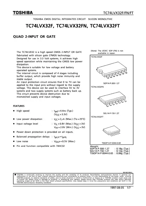
TC74LVX32F中文资料
- 格式:pdf
- 大小:236.44 KB
- 文档页数:7

74LCX374 Low Voltage Octal D-Type Flip-Flop with 5V Tolerant Inputs and Outputs74LCX374 Low Voltage Octal D-Type Flip-Flop with 5V Tolerant Inputs and Outputs74LCX374 Low Voltage Octal D-Type Flip-Flop with 5V Tolerant Inputs and OutputsAbsolute Maximum RatingsThe Absolute Maximum Ratings are those values beyond which the safety of the device cannot be guaranteed. The device should not be operated at these limits. The parametric values defined in the Electrical Characteristics tables are not guaranteed at the Absolute Maximum Ratings. The “Recommended Operating Conditions” table will define the conditions for actual device operation.Recommended Operating Conditions 5Notes:4.I O Absolute Maximum Rating must be observed.5.Unused inputs or I/Os must be held HIGH or LOW. They may not float.SymbolParameterConditions ValueUnitsV CC Supply Voltage − 0.5 to + 7.0V V I DC Input Voltage − 0.5 to + 7.0V V O DC Output Voltage Output in 3-ST A TE− 0.5 to + 7.0V Output in HIGH or LOW State 4 − 0.5 to V CC + 0.5I IK DC Input Diode Current V I < GND − 50mA I OK DC Output Diode Current V O < GND − 50mA V O > V CC+ 50I O DC Output Source/Sink Current ± 50mA I CC DC Supply Current per Supply Pin ± 100mA I GND DC Ground Current per Ground Pin ± 100mA T STGStorage T emperature− 65 to + 150° CSymbolParameterConditionsMin.Max.UnitsV CC Supply Voltage Operating2.03.6V Data Retention 1.5 3.6V I Input Voltage 0 5.5V V O Output Voltage HIGH or LOW State 0V CC V 3-ST A TE5.5I OH / I OLOutput CurrentV CC = 3.0V − 3.6V ± 24mAV CC = 2.7V − 3.0V ± 12V CC = 2.3V − 2.7V± 8T A Free-Air Operating T emperature − 4085 ° C ∆ t / ∆ VInput Edge RateV IN= 0.8V − 2.0V , V CC = 3.0V10ns / V74LCX374 Low Voltage Octal D-Type Flip-Flop with 5V Tolerant Inputs and OutputsDC Electrical CharacteristicsAC Electrical CharacteristicsNotes:6.Outputs disabled or 3-STATE only.7.Skew is defined as the absolute value of the difference between the actual propagation delay for any two separate outputs of thesame device. The specification applies to any outputs switching in the same direction, either HIGH-to-LOW (t OSHL ) or LOW-to-HIGH (t OSLH ).SymbolParameterConditionsV CC (V)T A = −40°C to +85°CUnitsMin.Max.V IH HIGH Level Input Voltage 2.3 − 2.7 1.7V2.7 −3.6 2.0V IL LOW Level Input Voltage 2.3 − 2.70.7V 2.7 − 3.60.8V OHHIGH Level Output VoltageI OH = −100µA 2.3 − 3.6V CC − 0.2VI OH = −8mA 2.3 1.8I OH = −12mA 2.7 2.2I OH = −18mA 3.0 2.4I OH = −24mA3.0 2.2V OLLOW Level Output VoltageI OL = 100µA 2.3 − 3.60.2VI OL = 8mA 2.30.6I OL = 12mA 2.70.4I OL = 16mA 3.00.4I OL = 24mA3.00.55I I Input Leakage Current 0 ≤ V I ≤ 5.5V 2.3 − 3.6±5.0µA I OZ 3-ST A TE Output Leakage 0 ≤ V O ≤ 5.5V , V I = V IH or V IL 2.3 − 3.6±5.0µA I OFF Power-Off Leakage Current V I or V O = 5.5V 010µA I CC Quiescent Supply Current V I = V CC or GND 2.3 − 3.610µA 3.6V ≤ V I , V O ≤ 5.5V 6 2.3 − 3.6±10∆I CCIncrease in I CC per InputV IH = V CC − 0.6V2.3 −3.6500µASymbolParameterT A = −40°C to +85°C, R L = 500 ΩUnitsV CC = 3.3V ± 0.3VV CC = 2.7V V CC = 2.5 ± 0.2C L = 50pFC L = 50pF C L = 30pF Min.Max.Min.Max.Min.Max.f MAX Maximum Clock Frequency 150150150MHz t PHL , t PLH Propagation Delay CP to O n1.58.5 1.59.5 1.510.5ns t PZL , t PZH Output Enable Time 1.58.5 1.59.5 1.510.5ns t PLZ , t PHZ Output Disable Time 1.57.51.58.51.59.0ns t S Setup Time 2.5 2.5 4.0ns t H Hold Time 1.5 1.5 2.0ns t W Pulse Width3.33.34.0ns t OSHL , t OSLHOutput to Output Skew 71.0ns74LCX374 Low Voltage Octal D-Type Flip-Flop with 5V Tolerant Inputs and OutputsDynamic Switching CharacteristicsCapacitanceSymbolParameterConditionsV CC (V)T A = 25°CUnitsTypicalV OLP Quiet Output Dynamic Peak V OL C L = 50pF , V IH = 3.3V , V IL = 0V 3.30.8V C L = 30pF , V IH = 2.5V , V IL = 0V 2.50.6V OLVQuiet Output Dynamic Valley V OLC L = 50pF , V IH = 3.3V , V IL = 0V 3.3−0.8VC L = 30pF , V IH = 2.5V , V IL = 0V2.5−0.6SymbolParameterConditionsTypicalUnitsC IN Input Capacitance V CC = Open, V I = 0V or V CC 7pF C OUT Output CapacitanceV CC = 3.3V , V I = 0V or V CC8pF C PDPower Dissipation CapacitanceV CC = 3.3V , V I = 0V or V CC , f = 10 MHz25pF74LCX374 Low Voltage Octal D-Type Flip-Flop with 5V Tolerant Inputs and Outputs74LCX374 Low Voltage Octal D-Type Flip-Flop with 5V Tolerant Inputs and Outputs74LCX374 Low Voltage Octal D-Type Flip-Flop with 5V Tolerant Inputs and OutputsTape and Reel SpecificationTape Format for DQFNTape Dimensions inches (millimeters)Reel Dimensions inches (millimeters)Package DesignatorTape SectionNumber CavitiesCavity StatusCover Tape StatusBQXLeader (Start End)125 (typ)Empty Sealed Carrier 3000Filled Sealed T railer (Hub End)75 (typ)EmptySealedTape SizeABCDNW1W212 mm13.0(330.0)0.059(1.50)0.512(13.00)0.795(20.20)2.165(55.00)0.488(12.4)0.724(18.4)74LCX374 Low Voltage Octal D-Type Flip-Flop with 5V Tolerant Inputs and Outputs Physical Dimensions inches (millimeters) unless otherwise noted20-Lead Small Outline Integrated Circuit (SOIC),JEDEC MS-013, 0.300" Wide Package Number M20B74LCX374 Low Voltage Octal D-Type Flip-Flop with 5V Tolerant Inputs and Outputs Physical Dimensions(Continued) inches (millimeters) unless otherwise notedPb-Free 20-Lead Small Outline Package (SOP),EIAJ TYPE II, 5.3mm Wide Package Number M20D74LCX374 Low Voltage Octal D-Type Flip-Flop with 5V Tolerant Inputs and Outputs Physical Dimensions(Continued) inches (millimeters) unless otherwise notedPb-Free 20-Terminal Depopulated Quad Very-Thin Flat Pack No Leads (DQFN),JEDEC MO-241, 2.5 x 4.5mm Package Number MLP020B74LCX374 Low Voltage Octal D-Type Flip-Flop with 5V Tolerant Inputs and OutputsPhysical Dimensions(Continued) inches (millimeters) unless otherwise notedJEDEC MO-150, 5.3mm Wide Package Number MSA2074LCX374 Low Voltage Octal D-Type Flip-Flop with 5V Tolerant Inputs and Outputs Physical Dimensions(Continued) inches (millimeters) unless otherwise noted20-Lead Thin Shrink Small Outline Package (TSSOP),JEDEC MO-153, 4.4mm Wide Package Number MTC2074LCX374 Low Voltage Octal D-Type Flip-Flop with 5V Tolerant Inputs and Outputs。


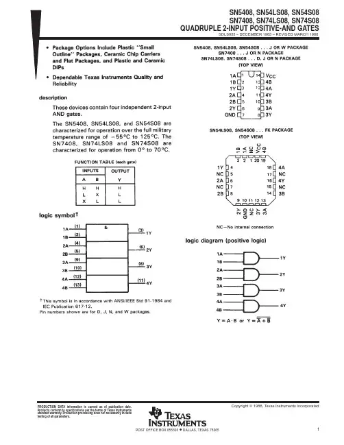
74HC32Quad 2−Input OR GateHigh−Performance Silicon−Gate CMOS The 74HC32 is identical in pinout to the LS32. The device inputs are compatible with Standard CMOS outputs; with pullup resistors, they are compatible with LSTTL outputs.Features•Output Drive Capability: 10 LSTTL Loads•Outputs Directly Interface to CMOS, NMOS and TTL •Operating V oltage Range: 2.0 to 6.0 V•Low Input Current: 1.0 m A•High Noise Immunity Characteristic of CMOS Devices•In Compliance With the JEDEC Standard No. 7A Requirements •ESD Performance: HBM > 2000 V; Machine Model > 200 V •Chip Complexity: 48 FETs or 12 Equivalent Gates•These are Pb−Free DevicesMARKINGDIAGRAMSHC32= Device CodeA= Assembly LocationL, WL= Wafer LotY= YearW, WW= Work WeekG or G= Pb−Free PackageTSSOP−14DT SUFFIXCASE 948GSOIC−14D SUFFIXCASE 751AHC32ALYW GG114See detailed ordering and shipping information in the package dimensions section on page 2 of this data sheet.ORDERING INFORMATION(Note: Microdot may be in either location)3Y11A1PIN 14 = V CC PIN 7 = GNDLOGIC DIAGRAM2B16Y24A25B28Y39A310B311Y412A413B4Y = A+BPinout: 14−Lead Packages (Top View)1314121110982134567V CC B4A4Y4B3A3Y3A1B1Y1A2B2Y2GNDL L H HL H L HFUNCTION TABLEInputs Output A B L H H HY ORDERING INFORMATIONDevicePackage Shipping †74HC32DR2G SOIC −14(Pb −Free)2500 / Tape & Reel74HC32DTR2GTSSOP −14*†For information on tape and reel specifications, including part orientation and tape sizes, please refer to our Tape and Reel Packaging Specifications Brochure, BRD8011/D.*This package is inherently Pb −Free.MAXIMUM RATINGSSymbol Parameter Value Unit V CC DC Supply Voltage (Referenced to GND)– 0.5 to + 7.0V V in DC Input Voltage (Referenced to GND)– 0.5 to V CC + 0.5V V out DC Output Voltage (Referenced to GND)– 0.5 to V CC + 0.5VI in DC Input Current, per Pin±20mAI out DC Output Current, per Pin±25mAI CC DC Supply Current, V CC and GND Pins±50mAP D Power Dissipation in Still Air,SOIC Package†TSSOP Package†500450mWT stg Storage Temperature– 65 to + 150_CT L Lead Temperature, 1 mm from Case for 10 SecondsSOIC or TSSOP Package260_CStresses exceeding Maximum Ratings may damage the device. Maximum Ratings are stressratings only. Functional operation above the Recommended Operating Conditions is not implied.Extended exposure to stresses above the Recommended Operating Conditions may affectdevice reliability.†Derating—SOIC Package: – 7 mW/_C from 65_ to 125_CTSSOP Package: − 6.1 mW/_C from 65_ to 125_CFor high frequency or heavy load considerations, see Chapter 2 of the ON Semiconductor High−Speed CMOS Data Book (DL129/D). RECOMMENDED OPERATING CONDITIONSSymbol Parameter Min Max UnitV CC DC Supply Voltage (Referenced to GND) 2.0 6.0VV in, V out DC Input Voltage, Output Voltage (Referenced toGND)0V CC VT A Operating Temperature, All Package Types– 55+ 125_Ct r, t f Input Rise and Fall Time V CC = 2.0 V (Figure 1)V CC = 4.5 VV CC = 6.0 V 01000500400nsThis device contains protectioncircuitry to guard against damagedue to high static voltages or electricfields. However, precautions mustbe taken to avoid applications of anyvoltage higher than maximum ratedvoltages to this high−impedance cir-cuit. For proper operation, V in andV out should be constrained to therange GND v (V in or V out) v V CC.Unused inputs must always betied to an appropriate logic voltagelevel (e.g., either GND or V CC).Unused outputs must be left open.DC CHARACTERISTICS(Voltages Referenced to GND)V CC (V)Guaranteed LimitSymbol Parameter Condition−55 to 25°C≤85°C≤125°C UnitV IH Minimum High−Level Input Voltage V out = 0.1V or V CC−0.1V|I out| ≤ 20m A 2.03.04.56.01.502.103.154.201.502.103.154.201.502.103.154.20VV IL Maximum Low−Level Input Voltage V out = 0.1V or V CC− 0.1V|I out| ≤ 20m A 2.03.04.56.00.500.901.351.800.500.901.351.800.500.901.351.80VV OH Minimum High−Level OutputVoltage V in = V IH or V IL|I out| ≤ 20m A2.04.56.01.94.45.91.94.45.91.94.45.9VV in =V IH or V IL|I out| ≤ 2.4mA|I out| ≤ 4.0mA|I out| ≤ 5.2mA3.04.56.02.483.985.482.343.845.342.203.705.20V OL Maximum Low−Level OutputVoltage V in = V IH or V IL|I out| ≤ 20m A2.04.56.00.10.10.10.10.10.10.10.10.1VV in = V IH or V IL|I out| ≤ 2.4mA|I out| ≤ 4.0mA|I out| ≤ 5.2mA3.04.56.00.260.260.260.330.330.330.400.400.40I in Maximum Input Leakage Current V in = V CC or GND 6.0±0.1±1.0±1.0m AI CC Maximum Quiescent SupplyCurrent (per Package)V in = V CC or GNDI out = 0m A6.0 2.02040m ANOTE:Information on typical parametric values can be found in Chapter 2 of the ON Semiconductor High−Speed CMOS Data Book (DL129/D). AC CHARACTERISTICS(C L = 50pF, Input t r = t f = 6ns)V CC (V)Guaranteed LimitSymbol Parameter−55 to 25°C≤85°C≤125°C Unitt PLH, t PHL Maximum Propagation Delay, Input A or B to Output Y(Figures 1 and 2)2.03.04.56.07530151395401916110552219nst TLH, t THL Maximum Output Transition Time, Any Output(Figures 1 and 2)2.03.04.56.07527151395321916110362219nsC in Maximum Input Capacitance101010pF NOTE:For propagation delays with loads other than 50 pF, and information on typical parametric values, see Chapter 2 of the ON Semiconductor High−Speed CMOS Data Book (DL129/D).C PD Power Dissipation Capacitance (Per Buffer)*Typical @ 25°C, V CC = 5.0 V, V EE = 0 VpF20*Used to determine the no−load dynamic power consumption: P D = C PD V CC2f + I CC V CC. For load considerations, see Chapter 2 of the ON Semiconductor High−Speed CMOS Data Book (DL129/D).Figure 1. Switching WaveformsOUTPUT YINPUT A OR BC L **Includes all probe and jig capacitanceTESTFigure 2. Test CircuitYABFigure 3. Expanded Logic Diagram(1/4 of the Device)GNDV CCSOIC −14CASE 751A −03ISSUE HNOTES:1.DIMENSIONING AND TOLERANCING PER ANSI Y14.5M, 1982.2.CONTROLLING DIMENSION: MILLIMETER.3.DIMENSIONS A AND B DO NOT INCLUDE MOLD PROTRUSION.4.MAXIMUM MOLD PROTRUSION 0.15 (0.006)PER SIDE.5.DIMENSION D DOES NOT INCLUDE DAMBAR PROTRUSION. ALLOWABLE DAMBAR PROTRUSION SHALL BE 0.127(0.005) TOTAL IN EXCESS OF THE D DIMENSION AT MAXIMUM MATERIAL CONDITION.DIM MIN MAX MIN MAX INCHESMILLIMETERS A 8.558.750.3370.344B 3.80 4.000.1500.157C 1.35 1.750.0540.068D 0.350.490.0140.019F 0.40 1.250.0160.049G 1.27 BSC 0.050 BSC J 0.190.250.0080.009K 0.100.250.0040.009M 0 7 0 7 P 5.80 6.200.2280.244R0.250.500.0100.019____DIMENSIONS: MILLIMETERS*For additional information on our Pb −Free strategy and soldering details, please download the ON Semiconductor Soldering and Mounting Techniques Reference Manual, SOLDERRM/D.TSSOP −14CASE 948G −01ISSUE BDIM MIN MAX MIN MAX INCHESMILLIMETERS A 4.90 5.100.1930.200B 4.30 4.500.1690.177C −−− 1.20−−−0.047D 0.050.150.0020.006F 0.500.750.0200.030G 0.65 BSC 0.026 BSC H 0.500.600.0200.024J 0.090.200.0040.008J10.090.160.0040.006K 0.190.300.0070.012K10.190.250.0070.010L 6.40 BSC 0.252 BSC M0 8 0 8 NOTES:1.DIMENSIONING AND TOLERANCING PER ANSI Y14.5M, 1982.2.CONTROLLING DIMENSION: MILLIMETER.3.DIMENSION A DOES NOT INCLUDE MOLD FLASH, PROTRUSIONS OR GATE BURRS.MOLD FLASH OR GATE BURRS SHALL NOT EXCEED 0.15 (0.006) PER SIDE.4.DIMENSION B DOES NOT INCLUDE INTERLEAD FLASH OR PROTRUSION.INTERLEAD FLASH OR PROTRUSION SHALL NOT EXCEED 0.25 (0.010) PER SIDE.5.DIMENSION K DOES NOT INCLUDE DAMBAR PROTRUSION. ALLOWABLE DAMBAR PROTRUSION SHALL BE 0.08(0.003) TOTAL IN EXCESS OF THE K DIMENSION AT MAXIMUM MATERIAL CONDITION.6.TERMINAL NUMBERS ARE SHOWN FOR REFERENCE ONLY .7.DIMENSION A AND B ARE TO BE DETERMINED AT DATUM PLANE −W −.____14X REF K14X0.360.65PITCHSOLDERING FOOTPRINT**For additional information on our Pb −Free strategy and soldering details, please download the ON Semiconductor Soldering and Mounting Techniques Reference Manual, SOLDERRM/D.ON Semiconductor and are registered trademarks of Semiconductor Components Industries, LLC (SCILLC). SCILLC reserves the right to make changes without further notice to any products herein. SCILLC makes no warranty, representation or guarantee regarding the suitability of its products for any particular purpose, nor does SCILLC assume any liability arising out of the application or use of any product or circuit, and specifically disclaims any and all liability, including without limitation special, consequential or incidental damages.“Typical” parameters which may be provided in SCILLC data sheets and/or specifications can and do vary in different applications and actual performance may vary over time. All operating parameters, including “Typicals” must be validated for each customer application by customer’s technical experts. SCILLC does not convey any license under its patent rights nor the rights of others. SCILLC products are not designed, intended, or authorized for use as components in systems intended for surgical implant into the body, or other applications intended to support or sustain life, or for any other application in which the failure of the SCILLC product could create a situation where personal injury or death may occur. Should Buyer purchase or use SCILLC products for any such unintended or unauthorized application, Buyer shall indemnify and hold SCILLC and its officers, employees, subsidiaries, affiliates, and distributors harmless against all claims, costs, damages, and expenses, and reasonable attorney fees arising out of, directly or indirectly, any claim of personal injury or death associated with such unintended or unauthorized use, even if such claim alleges that SCILLC was negligent regarding the design or manufacture of the part. SCILLC is an Equal Opportunity/Affirmative Action Employer. This literature is subject to all applicable copyright laws and is not for resale in any manner.PUBLICATION ORDERING INFORMATION。