SP7656应用指南(高电压大电流DC-DC降压稳压器)
- 格式:pdf
- 大小:369.56 KB
- 文档页数:10
DATA SHEETSP122040V/8A同步降压DC/DC转换电路版本号:V1.0一.概述SP1220是一款降压型PWM控制器,该控制器可驱动双路输出8A(4A+4A)负载电流。
设计允许SP1220在9V到40V宽输入电压范围内工作。
通过将COMP/EN引脚逻辑电平拉低来实现外部关断功能,并进入待机模式。
外部补偿使反馈控制环路具有良好的线压调整率和负载调整率,且外围设计灵活。
SP1220可以工作在CC(恒流输出)或CV(恒压输出)两种模式,过流保护(OCP)电流值可以通过外部电流检测电阻设置。
SP1220适用于有限流要求的DC/DC开关电源,该芯片采用MSOP10封装,需要较少的外部器件。
二.特性z电压输入范围:9~40Vz输出电压精度(Vref=1.0V):±2.0%z双通道CC/CV模式z双通道外部限流z过温保护(OTP)z内置软启动时间3msz固定频率120KHzz输入欠压保护(最小7 V,典型7.5V,最大8V)z占空比范围:0~90%z一个引脚即可实现外部补偿和关断控制z输出可使用陶瓷电容z内置可调整的线压补偿z MSOP10封装三.应用z汽车充电器z高亮度照明z便携式设备供电电源z 具有限流功能的通用DC/DC 控制器四、极限参数(T A =25℃)参数 符号 值 单位 输入电压 Vin -0.3到+43 V BS 到LX -0.3到+7 V LX 到GND -1到+VIN+1 V BS,UG 到GNDVsw -0.3到Vsw +7 V FB,COMP,LG ,SEN1,SEN2到GND-0.3到+7V ESD HBM(人体模式) ±2K V ESD MM(机械模式) ±200 V 功耗,PD @T A =25℃PD (T J –T A )/θJA W 热阻θJC 43 ℃/W 从结到环境的热阻θJA 135 ℃/W注:器件工作条件超过上表中列出的范围时可能造成器件的永久损坏或功能异常。
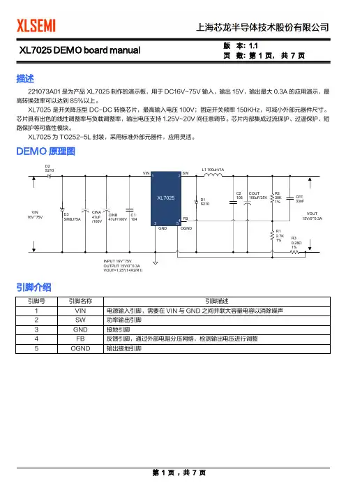
页数:第1 页,共7 页描述221073A01是为产品XL7025制作的演示板,用于DC16V~75V输入,输出15V,输出最大0.3A的应用演示,最高转换效率可以达到85%以上。
XL7025是开关降压型DC-DC转换芯片,最高输入电压100V;固定开关频率150KHz,可减小外部元器件尺寸。
芯片具有出色的线性调整率与负载调整率,输出电压支持1.25V~20V间任意调节。
芯片内部集成过流保护、过温保护、短路保护等可靠性模块。
XL7025为TO252-5L封装,采用标准外部元器件,应用灵活。
DEMO原理图D2VOUT=1.25*(1+R2/R1)引脚介绍页数:第2 页,共7 页物料清单2.CINA、D3用于输入尖峰电压吸收。
性能数据转换效率(不包含输入防反接部分电路)页 数:第 3 页, 共 7 页转换效率: 线性调整率和负载调整率:0.100.150.200.250.3020253035404550556065707580859095Efficiency VS Output currentE f f i c i e n c y (%)Ouput current(A) VIN=24V,VOUT=15V,IOUT=0.1~0.3A VIN=36V,VOUT=15V,IOUT=0.1~0.3A VIN=48V,VOUT=15V,IOUT=0.1~0.3A VIN=60V,VOUT=15V,IOUT=0.1~0.3A VIN=72V,VOUT=15V,IOUT=0.1~0.3A0.100.150.200.250.3014.214.414.614.815.015.215.415.615.8Output voltage VS Output currentO u t p u t v o l t a g e (V )Output current(mA)VIN=24V,VOUT=15V,IOUT=0.1A~0.3A VIN=36V,VOUT=15V,IOUT=0.1A~0.3A VIN=48V,VOUT=15V,IOUT=0.1A~0.3A VIN=60V,VOUT=15V,IOUT=0.1A~0.3A VIN=72V,VOUT=15V,IOUT=0.1A~0.3A热插拔上电输出电压波形:VIN=36VIOUT=0AIOUT=0.3AVIN=48VIOUT=0AIOUT=0.3A页数:第4 页,共7 页VIN=60VIOUT=0A IOUT=0.3A蓝色通道:输入电压波形,10V/格;紫色通道:输出电压波形,5V/格;秒格:1mS/格。
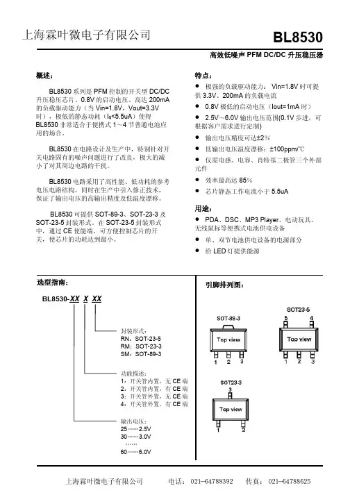
高效低噪声PFM DC/DC 升压稳压器BL8530概述:BL8530系列是PFM 控制的开关型DC/DC 升压稳压芯片。
0.8V 的启动电压、高达200mA的负载驱动能力(当Vin=1.8V ,Vout=3.3V 时),极低的静态功耗(I q <5.5uA )使得BL8530非常适合于便携式1~4节普通电池应用的场合。
BL8530在电路设计及生产中,特别针对开关电路固有的噪声问题进行了改良,极大的减小了对其周边电路的干扰。
BL8530电路采用了高性能、低功耗的参考电压电路结构,同时在生产中引入修正技术,保证了输出电压的高输出精度及低温度漂移。
BL8530可提供SOT-89-3、SOT-23-3及SOT-23-5封装形式。
在SOT-23-5封装形式中,通过CE 使能端,可方便控制芯片的开关,使芯片的功耗达到最小。
特点:• 极强的负载驱动能力: Vin=1.8V 时可提供3.3V 、200mA 的负载电流• 0.8V 极低的启动电压(Iout=1mA 时)• 2.5V ~6.0V 输出电压范围(0.1V 步进,可根据客户需求进行定制) • 输出电压精度可达±2%• 低输出电压温度漂移:±100ppm/℃• 仅需电感、电容、肖特基二极管三个外部元件• 效率最高达85%• 芯片静态工作电流小于5.5uA用途:• PDA 、DSC 、MP3 Player 、电动玩具、无线鼠标等便携式电池供电设备 • 单、双节电池供电设备的电源部分 •给LED 灯提供能源上海霖叶微电子有限公司 BL8530引脚定义表引脚号符号引脚描述SOT-89-3SOT-23-3 SOT-23-51 1 4 Vss(GND)接地引脚2 2 2 Vout输出电压监测,内部电路供电引脚3 3 5 Lx(Ext)开关引脚-- 3 NC 空脚-- 1 CE 使能端产品命名目录产品名称输出电压规格开关管 CE端封装形式V 内置无SOT-89-3BL8530-XX1SM XXBL8530-XX1RM XXV 内置无SOT-23-3V 内置有SOT-23-5BL8530-XX2RN XXBL8530-XX3SM XXV 外置无SOT-89-3BL8530-XX3RM XXV 外置无SOT-23-3BL8530-XX4RN XXV 外置有SOT-23-5系统框图:产品的极限参数输入电压------------------------------------------------------------------------------------------------0.3V~12VLx脚开关电压------------------------------------------------------------------------------------------0.3V~(Vout+0.3) CE脚电压-----------------------------------------------------------------------------------------------0.3V~(Vout+0.3) Lx脚输出电流-----------------------------------------------------------------------------------------0.7A允许的最大功耗,Pd T=25°CSOT-89-3------------------------------------------------------------------------------------------0. 5WSOT-23-5------------------------------------------------------------------------------------------0.15WSOT-23-3------------------------------------------------------------------------------------------0.15W最大工作结温-----------------------------------------------------------------------------------------150°C工作温度----------------------------------------------------------------------------------------------- -20~+80°C存贮温度----------------------------------------------------------------------------------------------- -40~125°C焊接温度和时间--------------------------------------------------------------------------------------260°C,10S推荐工作条件名称最小 推荐 最大 单位输入电压范围 0.8 Vout V 电感值10 27 100 µH 输入电容值 0 ≥10µF 输出电容值* 47 100 220 µF 工作环境温度 -20 85 ℃*:建议使用钽电容以减小输出电压的开关纹波。
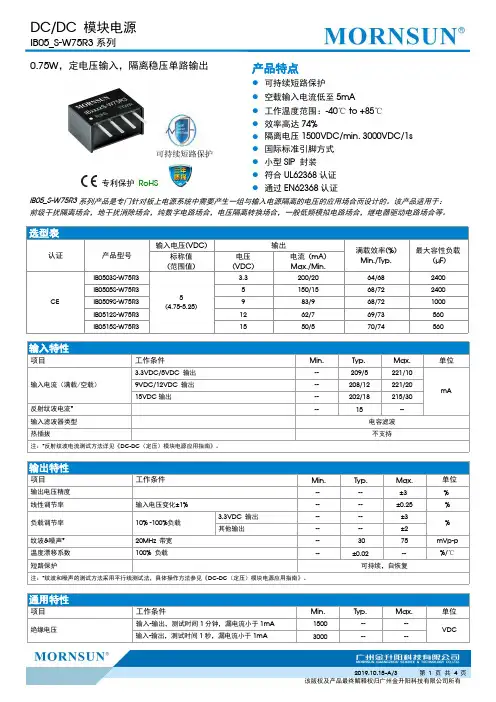
选型表认证产品型号输入电压(VDC)输出满载效率(%)Min./Typ.最大容性负载(µF)标称值(范围值)电压(VDC)电流(mA)Max./Min.CEIB0503S-W75R35(4.75-5.25)3.3200/2064/682400IB0505S-W75R35150/1568/722400IB0509S-W75R3983/968/721000IB0512S-W75R31262/769/73560IB0515S-W75R31550/570/74560输入特性项目工作条件Min.Typ.Max.单位输入电流(满载/空载)3.3VDC/5VDC 输出--209/5221/10mA9VDC/12VDC 输出--208/12221/2015VDC 输出--202/18215/30反射纹波电流*--15--输入滤波器类型电容滤波热插拔不支持注:*反射纹波电流测试方法详见《DC-DC (定压)模块电源应用指南》。
输出特性项目工作条件Min.Typ.Max.单位输出电压精度----±3%线性调节率输入电压变化±1%----±0.25%负载调节率10%-100%负载 3.3VDC 输出----±3%其他输出----±2纹波&噪声*20MHz 带宽--3075mVp-p 温度漂移系数100%负载--±0.02--%/℃短路保护可持续,自恢复注:*纹波和噪声的测试方法采用平行线测试法,具体操作方法参见《DC-DC (定压)模块电源应用指南》。
通用特性项目工作条件Min.Typ.Max.单位绝缘电压输入-输出,测试时间1分钟,漏电流小于1mA 1500----VDC输入-输出,测试时间1秒,漏电流小于1mA3000----0.75W ,定电压输入,隔离稳压单路输出专利保护RoHS产品特点●可持续短路保护●空载输入电流低至5mA ●工作温度范围:-40℃to +85℃●效率高达74%●隔离电压1500VDC/min,3000VDC/1s ●国际标准引脚方式●小型SIP 封装●符合UL62368认证●通过EN62368认证IB05_S-W75R3系列产品是专门针对板上电源系统中需要产生一组与输入电源隔离的电压的应用场合而设计的。
1 索引 页次1.产品介绍................................................................ 1 2产品规格................................................................ 2 2-1.一般规格............................................................. 2 2-2.定电压操作........................................................ . 3 2-3.定电流操作......................................................... 3 2-4.数位式指示表头................................................... 3 2-5.过电压保护......................................................... 3 2-6.绝缘度............................................................... 3 3.动作原理................................................................ 4 4.面板介绍................................................................ 7 4-1.前面板............................................................... 7 4-2.后面板............................................................... 7 5.操作说明................................................................10 5-1.使用前注意事项...................................................10 5-2.设定限流值.........................................................10 5-3.定电压/定电流之交越特性.......................................11 5-4.操作模式............................................................12 6一般维修................................................................13 6-1.保险丝之更换......................................................13 6-2.电源电压变换......................................................13 6-3.校正方法............................................................14 6-4.清洁方法 (15)1产品介绍本系列产品是属于仪器用的交换式直流电源供应器,改善了传统线性式电源供应器体积大、重量重、和效率差的缺点。

DAC7565中文简明手册12位,四通道,低脉冲干扰,电压输出,2.5V内部参考电压模数转换器特性:相对精度:0.5LSB故障能量:0.15nV-s内部参考电压:2.5V默认;初始精度0.004%;温漂2-5ppm/Oc;20mA源能力;上电复位到0标度或中间标度;异步清除到0标度或中间标度;超低功耗1mA (5V时)宽电压范围2.7-5.5V温度范围内12位单调稳定时间10uS到±0.024%全范围低功耗串行口带施密特输入最高50MHz片内输出缓冲放大器,带轨到轨操作1.8-5.5V逻辑兼容温度范围-40到+105度应用范围:便携式仪器;闭环伺服控制;过程控制PLC;数据采集系统;可编程衰减;电脑外设。
相关器件16-BIT 14-BIT 12-BIT引脚功能兼容DAC8565 DAC8165 DAC7565功能兼容DAC8564 DAC8164 DAC7564描述:DAC7565是低功耗,电压输出、四通道12位数模转换器。
该设备包括一个2.5 v内部参考电压(默认启用),给2.5 v的全范围输出电压。
内部参考的初始精度0.02%,可以在VREFH/ VREFOUT引脚提供20mA电路。
该设备是单调的,提供了很好的线性,和最小码到码瞬态干扰电压(故障)。
DAC7565使用多功能3-wire串行接口最高50 mhz的时钟频率。
接口是兼容标准SPI QSPI, Microwire,和数字信号处理器的接口。
DAC7565包含上电复位电路,保证了DAC输出电压在0档或中档,直到一个有效的代码写入设备。
该设备包含一个省电功能,通过串行接口,减少设备的电流1.3μa在 5 v时。
功耗在3 v 时2.9 mw, 省电模式减少到1.5μw。
内部参考,低功耗和小封装让这个设备适合便携式电池供电设备。
DAC7565 向下引脚兼容和功能兼容DAC8165 DAC8565,和功能兼容DAC7564 DAC8164 DAC8564。
AD7656中文资料AD7656—16位同步采样双极ADC转换器功能:6路独立的16位AD6路真双极模拟量输入引脚/软件可选择的范围:±10V,±5V快速通过率250KSPS指定Vcc为4.5V~5.5V低功耗以5V 供应250 kSPS的160 mW宽的输入带宽: 输入频率为100kHz时信噪比为85dB在片参考和参考缓冲器并行和串行接口高速串行接口SPI/ QSPI/μWire/DSP可兼容无流水线延迟备用模式:最大0.5μA64LQFP封装应用电力线检测系统仪器和控制系统多轴定位系统一般描述AD7656芯片包含6路16位快速、低功耗、逐步逼近ADC。
元件工作电源4.5V~5.5V,具有250kSPS通过率特性。
元件具有低噪音、宽带宽跟踪保持放大器,能够操作输入频率达到8MHz。
转换过程和数据采集由 CONVST 信号和一个内部振荡器控制。
三个CONVST引脚允许三对ADC独立的同时采样。
AD7656具有高速的并行和串行接口,可以与微处理器和DSP接口。
AD7656具有菊花链特性,允许多个ADC与一个串行接口连接。
元件没有流水线延迟。
AD7656在±10V范围内能提供真双极的输入信号。
AD7656包含一个2.5V内部参考电压,也能采用一个外部考电压,如果V REF引脚供应一个3V外部叁考电压, ADC能供给真双极±12V模拟量输入范围。
参照这±12V输入范围,需要给V DD和V SS提供±12V电压。
产品特点1 6路16位250kSPS ADC2 6路真双极高阻抗模拟量输入3 具有一个并行和一个高速串行接口。
引脚功能描述术语积分非线性这是从一条直线横传过ADC传递函数终点的最大的偏差。
传递函数终点是零刻度时,1/2LSB点低于最初代码转换,是满刻度时,1/2LSB点超出最后代码转换。
差分非线性这是一个在ADC转换中任何两个邻近代码的LSB转换的测量值与理论值差。
该型机电源电路采用了待机功耗很低的LD7575作为电源控制芯片。
它通常应用在新型的17、19英寸液晶显示器电源电路中。
除了AOC H912W+显示器外。
采用LD7575作为电源控制芯片的还有美格WB9、清华同方XP911W、联想LXM -WL19AH/WL19CH/WL19BH、联想HKC 988A+、海尔HT-19307/22306W等机型。
LD7575有SOP-8(LD7575 PS)和DIP-8(LD7575 PN)两种封装形式。
其内部电路框图如上图所示,各引脚功能如附表所示。
一、电源电路原理LD7575在AOC H912W+液晶显示器中的实际应用电路如下图所示。
LD7575用203D6代用要改启动电阻,LD7575可以用1200AP40,LD7575ps直接代用1.整流滤波电路220V交流电压经过共态扼流圈L901、L902、跨接线路电容C909进行EMI滤波。
其中C909用于滤除低频正态噪声。
R900、R902用于拔掉电源时对电容C909起放电作用。
220V交流经BD901桥式整流输出波动直流电经滤波电容C907滤波后,生成310V的直流电压。
负温度系数热敏电阻NRgOI用来限制启动时的电流。
防止启动电流过大烧毁保险丝。
2.启动/振荡电路刚启动开关电源时,IC901(LD7575PS)所需的启动工作电压由,±310V直流电压经过R905限流后加至IC901(8)脚实现开机启动操作。
LD7575PS开始工作后。
其(5)脚输出PWM脉冲波(该脉冲控制功率管Q900并按其工作频率进行开关动作)。
Q900工作在开关状态后,开关变压器T901在次级绕组输出整机需要的各种供电电压。
‘开关变压器T901的(1)-(3)绕组产生的高频电压经R610限流、D901整流、C911滤波后。
直接输入至LD7575PS的(6)脚作为正常工作状态的供电电压。
在正常工作时。
其LD7575PS的(6)脚必须有,14V左右的电压为芯片供电。
AD7656的原理及在继电保护产品中的应用1 AD7656的性能简介AD7656是高集成度、6通道、16bit逐次逼近(SAR)型ADC,它具有最大4 LSBS INL和每通道达250kSPS的采样率,并且在片内包含一个2.5V内部基准电压源和基准缓冲器。
该器件仅有典型值160mW的功耗,比最接近的同类双极性输入ADC的功耗降低了60%。
AD7656包含一个低噪声、宽带采样保持放大器(T/H),以便处理输入频率高达8MHz的信号。
该AD7656还具有高速并行和串行接口,可以与微处理器(MCU)或数字信号处理器(DSP)连接。
AD7656在串行接口方式下,能提供一个菊花链连接方式,以便把多个ADC连接到一个串行接口上。
AD7656采用具有ADI专利技术的iCMOS(工业CMOS)工艺。
iCMOS 工艺是一种高压半导体工艺与亚微米CMOS(互补金属氧化物半导体)和互补双极型工艺相结合的制造上艺。
它能开发出承受30V电源电压的多种高性能模拟IC,并且其小封装尺寸是任何其他同类高电压IC都未曾达到的。
与使用传统CMOS工艺的模拟IC不同,iCMOS器件能承受高电源电压,同时提高性能、显著降低功耗和缩小封装尺寸。
AD7656是使用该种工艺设计制造的产品,所以非常适合在继电保护、电机控制等工业领域使用。
图1是AD7656的内部原理框图。
2 AD7656的工作原理AD7656足具有独立的六通道逐次逼近型(SAR)的模数转换器,转换处理和数据的精度是通过CONVST信号和一个内部晶振控制的。
3个CONVST管脚允许3路ADC对独立同步采样。
当3个CONVST管脚连接到一起时,就可以进行6个通道的同步采样。
AD7656具有高速的并行和串行接口,允许其与Microprocessors和DSP进行接口。
当使用串行接口模式时,AD7656具有的菊花链特性允许多个ADC和一个串行接口连接。
由于在电力继电保护产品中以并行接口连接设计为主,所以下面将以并行接口的连接方式介绍其工作原理。
EVALUATION KIT AVAILABLE3.3V/5V/Adjustable-Output,Step-Up DC-DC Converters_______________General DescriptionThe MAX756/MAX757 are CMOS step-up DC-DC switch-ing regulators for small, low input voltage or battery-pow-ered systems. The MAX756 accepts a positive input voltage down to 0.7V and converts it to a higher pin-selectable output voltage of 3.3V or 5V. The MAX757 is an adjustable version that accepts an input voltage down to 0.7V and generates a higher adjustable output voltage in the range from 2.7V to 5.5V. Typical full-load efficiencies for the MAX756/MAX757 are greater than 87%.The MAX756/MAX757 provide three improvements over previous devices. Physical size is reduced—the high switching frequencies (up to 0.5MHz) made possible by MOSFET power transistors allow for tiny (<5mm diameter)surface-mount magnetics. Efficiency is improved to 87%(10% better than with low-voltage regulators fabricated in bipolar technology). Supply current is reduced to 60µA by CMOS construction and a unique constant-off-time pulse-frequency modulation control scheme.________________________Applications3.3V to 5V Step-Up Conversion Palmtop ComputersPortable Data-Collection EquipmentPersonal Data Communicators/Computers Medical Instrumentation2-Cell & 3-Cell Battery-Operated Equipment Glucose Meters* Dice are tested at T A = +25°C only._________________Pin Configurations__________Typical Operating CircuitMAX756/MAX7573.3V/5V/Adjustable-Output,Step-Up DC-DC ConvertersSupply Voltage (OUT to GND)....................................-0.3V, +7V Switch Voltage (LX to GND)........................................-0.3V, +7V Auxiliary Pin Voltages (SHDN, LBI, LBO, REF,3/5, FB to GND)........................................-0.3V, (V OUT + 0.3V)Reference Current (I REF )....................................................2.5mA Continuous Power Dissipation (T A = +70°C)Plastic DIP (derate 9.09mW/°C above +70°C).............727mW SO (derate 5.88mW/°C above +70°C)..........................471mWOperating Temperature Ranges:MAX75_C_ _........................................................0°C to +70°C MAX75_E_ _......................................................-40°C to +85°C Junction Temperature......................................................+150°C Storage Temperature Range...............................-65°to +160°C Lead Temperature (soldering, 10sec)...........................+300°CELECTRICAL CHARACTERISTICS(Circuits of Figure 1 and Typical Operating Circuit, V IN = 2.5V, I LOAD = 0mA, T A = T MIN to T MAX , unless otherwise noted.)Stresses beyond those listed under “Absolute Maximum Ratings" may cause permanent damage to the device. These are stress ratings only, and functional operation of the device at these or any other conditions beyond those indicated in the operational sections of the specifications is not implied. Exposure to absolute maximum rating conditions for extended periods may affect device reliability.ABSOLUTE MAXIMUM RATINGSNote 1:Supply current from the 3.3V output is measured with an ammeter between the 3.3V output and OUT pin. This currentcorrelates directly with actual battery supply current, but is reduced in value according to the step-up ratio and efficiency.Note 2:Minimum value is production tested. Maximum value is guaranteed by design and is not production tested.MAX756/MAX7573.3V/5V/Adjustable-Output,Step-Up DC-DC ConvertersMINIMUM START-UP INPUT VOLTAGEvs. LOAD CURRENTLOAD CURRENT (mA)S T A R T -U P I N P U T V O L T A G E (V )10100100011.81.61.41.21.00.8400.1101000EFFICIENCY vs. LOAD CURRENT3.3V OUTPUT MODELOAD CURRENT (mA)E F F I C I E N C Y (%)60809050701100400.1101000EFFICIENCY vs. LOAD CURRENT5V OUTPUT MODELOAD CURRENT (mA)E F F I C I E N C Y (%)60809050701100800002MAXIMUM OUTPUT CURRENTvs. INPUT VOLTAGE200600INPUT VOLTAGE (V)M A X I M U M O U T P U T C U R R E N T (m A )44001003005007001351M 1010μ10m1SWITCHING FREQUENCY vs. LOAD CURRENT100LOAD CURRENT (A)S W I T C H I N G F R E Q U E N C Y (H z )1k10k100k 100μ1m100m02QUIESCENT CURRENT vs. INPUT VOLTAGEINPUT VOLTAGE (V)Q U I E S C E N T C U R R E N T (μA )410020030040050013550125SHUTDOWN QUIESCENT CURRENTvs. INPUT VOLTAGE20INPUT VOLTAGE (V)S H U T D O W N Q U I E S C E N T C U R R E N T (μA )440103031000REFERENCE VOLTAGE LOAD REGULATION28LOAD CURRENT (μA)V R E F L O A D R E G U L A T I O N (m V )6450100150200250__________________________________________Typical Operating Characteristics(Circuit of Figure 1, T A = +25°C, unless otherwise noted.)MAX756/MAX7573.3V/5V/Adjustable-Output,Step-Up DC-DC Converters______________________________________________________________Pin DescriptionOUTPUT VOLTAGE 50mV/divV IN = 2.5VHORIZONTAL = 50μs/div 5V Mode LOAD-TRANSIENT RESPONSEOUTPUT CURRENT 0mA to 200mA_____________________________Typical Operating Characteristics (continued)(Circuit of Figure 1, T A = +25°C, unless otherwise noted.)V SHDN 2V/divV IN = 2.5VHORIZONTAL = 5ms/div 5V ModeSTART-UP DELAYV OUT 2V/div3V0V 5V0VMAX756/MAX7573.3V/5V/Adjustable-Output, Step-Up DC-DC Converters_______________Detailed DescriptionOperating Principle The MAX756/MAX757 combine a switch-mode regulator with an N-channel MOSFET, precision voltage reference, and power-fail detector in a single monolithic device. The MOSFE T is a “sense-FE T” type for best efficiency, and has a very low gate threshold voltage to ensure start-up under low-battery voltage conditions (1.1V typ).Pulse-FrequencyModulation Control Scheme A unique minimum off time, current-limited, pulse-frequen-cy modulation (PFM) control scheme is a key feature of the MAX756/MAX757. This PFM scheme combines the advantages of pulse-width modulation (PWM) (high output power and efficiency) with those of a traditional PFM pulse-skipper (ultra-low quiescent currents). There is no oscillator; at heavy loads, switching is accomplished through a constant peak-current limit in the switch, which allows the inductor current to self-oscillate between this peak limit and some lesser value. At light loads, switching frequency is governed by a pair of one-shots, which set a minimum off-time (1µs) and a maximum on-time (4µs). The switching frequency depends on the load and the input voltage, and can range as high as 500kHz.The peak switch current of the internal MOSFET power switch is fixed at 1A ±0.2A. The switch's on resistance is typically 0.5Ω, resulting in a switch voltage drop (V SW) of about 500mV under high output loads. The value of V SW decreases with light current loads. Conventional PWM converters generate constant-fre-quency switching noise, whereas this architecture pro-duces variable-frequency switching noise. However, the noise does not exceed the switch current limit times the filter-capacitor equivalent series resistance (E SR), unlike conventional pulse-skippers.Voltage Reference The precision voltage reference is suitable for driving external loads such as an analog-to-digital converter. It has guaranteed 250µA source-current and 20µA sink-current capability. The reference is kept alive even in shutdown mode. If the reference drives an external load, bypass it with 0.22µF to GND. If the ref-erence is unloaded, bypass it with at least 0.1µF.Control-Logic Inputs The control inputs (3/5, SHDN) are high-impedance MOS gates protected against ESD damage by normally reverse-biased clamp diodes. If these inputs are dri-ven from signal sources that exceed the main supply voltage, the diode current should be limited by a series resistor (1MΩsuggested). The logic input threshold level is the same (approximately 1V) in both 3.3V and 5V modes. Do not leave the control inputs floating.__________________Design ProcedureOutput Voltage Selection The MAX756 output voltage can be selected to 3.3V or 5V under logic control, or it can be left in one mode or the other by tying 3/5to GND or OUT. Efficiency varies depending upon the battery and the load, and is typi-cally better than 80% over a 2mA to 200mA load range. The device is internally bootstrapped, with power derived from the output voltage (via OUT). When the output is set at 5V instead of 3.3V, the higher internal supply voltage results in lower switch-transistor on resistance and slightly greater output power. Bootstrapping allows the battery voltage to sag to less than 1V once the system is started. Therefore, the bat-tery voltage range is from V OUT+ V D to less than 1V (where V D is the forward drop of the Schottky rectifier). If the battery voltage exceeds the programmed output voltage, the output will follow the battery voltage. In many systems this is acceptable; however, the output voltage must not be forced above 7V.The output voltage of the MAX757 is set by two resis-tors, R1 and R2 (Figure 1), which form a voltage divider between the output and the FB pin. The output voltage is set by the equation:V OUT= (V REF) [(R2 + R1) / R2]where V REF= 1.25V.To simplify resistor selection:R1 = (R2) [(V OUT/ V REF) - 1]Since the input bias current at FB has a maximum value of 100nA, large values (10kΩto 200kΩ) can be used for R1 and R2 with no significant loss of accuracy. For 1% error, the current through R1 should be at least 100 times FB’s bias current.Low-Battery Detection The MAX756/MAX757 contain on-chip circuitry for low-battery detection. If the voltage at LBI falls below the reg-ulator’s internal reference voltage (1.25V), LBO (an open-drain output) sinks current to GND. The low-battery mon-itor's threshold is set by two resistors, R3 and R4 (Figure 1), which forms a voltage divider between the input volt-age and the LBI pin. The threshold voltage is set by R3 and R4 using the following equation:R3 = [(V IN/ V REF) - 1] (R4)MAX756/MAX7573.3V/5V/Adjustable-Output,Step-Up DC-DC ConvertersIN detector, R3 and R4 are the input divider resistors at LBI, and V REF is the internal 1.25V reference.Since the LBI current is less than 100nA, large resistor values (typically 10k Ωto 200k Ω) can be used for R3and R4 to minimize loading of the input supply.When the voltage at LBI is below the internal threshold,LBO sinks current to GND. A pull-up resistor of 10k Ωor more connected from LBO to V OUT can be used when driving CMOS circuits. Any pull-up resistor con-nected to LBO should not be returned to a voltage source greater than V OUT . When LBI is above the threshold, the LBO output is off. The low-battery com-parator and reference voltage remain active when the MAX756/MAX757 is in shutdown mode.If the low-battery comparator is not used, connect LBI to V IN and leave LBO open.Inductor SelectionThe inductors should have a saturation (incremental)current rating equal to or greater than the peak switch-current limit, which is 1.2A worst-case. However, it’s generally acceptable to bias the inductor into satura-tion by 20%, although this will reduce the efficiency.The 22µH inductor shown in the typical applications cir-cuit is sufficient for most MAX756/MAX757 application circuits. Higher input voltages increase the energy transferred with each cycle, due to the reduced input/output differential. Minimize excess ripple due to increased energy transfer by reducing the inductorvalue (10µH suggested).The inductor’s DC resistance significantly affects effi-ciency. For highest efficiency, limit L1’s DC resistance to 0.03Ωor less. See Table 1 for a list of suggested inductor suppliers.Table 1. Component SuppliersAVXUSA:(207) 282-5111, FAX (207) 283-1941(800) 282-9975CoilCraft USA:(708) 639-6400, FAX (708) 639-1969Coiltronics USA:(407) 241-7876, FAX (407) 241-9339CollmerSemiconductor USA:(214) 233-1589Motorola USA:(602) 244-3576, FAX (602) 244-4015NichiconUSA:(708) 843-7500, FAX (708) 843-2798Japan:+81-7-5231-8461, FAX (+81-) 7-5256-4158Nihon USA:(805) 867-2555, FAX (805) 867-2556Japan:+81-3-3494-7411, FAX (+81-) 3-3494-7414Sanyo OS-CON USA:(619) 661-6835Japan:+81-720-70-1005, FAX (+81-720-) 70-1174Sprague USA:(603) 224-1961, FAX (603) 224-1430Sumida USA:(708) 956-0666Japan:+81-3-3607-5111, FAX (+81-3-) 3607-5428UnitedChemi-Con USA:(708) 696-2000, FAX (708) 640-6311Capacitor SelectionA 100µF, 10V surface-mount (SMT) tantalum capacitor typically provides 50mV output ripple when stepping up from 2V to 5V at 200mA. Smaller capacitors, down to 10µF, are acceptable for light loads or in applica-tions that can tolerate higher output ripple.MAX756/MAX7573.3V/5V/Adjustable-Output,Step-Up DC-DC ConvertersFigure 2. MAX756 Block DiagramThe E SR of both bypass and filter capacitors affects efficiency. Best performance is obtained by using spe-cialized low-ESR capacitors, or connecting two or more filter capacitors in parallel. The smallest low-ESR SMT tantalum capacitors currently available are Sprague 595D series, which are about half the size of competing products. Sanyo OS-CON organic semiconductor through-hole capacitors also exhibit very low ESR, and are especially useful for operation at cold tempera-tures. Table 1 lists suggested capacitor suppliers.Rectifier DiodeFor optimum performance, a switching Schottky diode,such as the 1N5817, is recommended. 1N5817 equiv-alent diodes are also available in surface-mount pack-ages from Collmer Semiconductor in Dallas, TX, phone (214) 233-1589. The part numbers are SE 014 or SE024. For low output power applications, a pn junc-tion switching diode, such as the 1N4148, will also work well, although efficiency will suffer due to the greater forward voltage drop of the pn junction diode.MAX756/MAX7573.3V/5V/Adjustable-Output 3.3V/5V/Adjustable-Output,Step-Up DC-DC Converters3/5 (MAX756)FB (MAX757)REFSHDN___________________Chip Topography________________________________________________________Package InformationPC Layout and GroundingThe MAX756/MAX757 high peak currents and high-fre-quency operation make PC layout important for mini-mizing ground bounce and noise. The distance between the MAX756/MAX757’s GND pin and the ground leads of C1 and C2 in Figure 1 must be kept to less than 0.2" (5mm). All connections to the FB and LX pins should also be kept as short as possible. To obtain maximum output power and efficiency and mini-mum output ripple voltage, use a ground plane and solder the MAX756/MAX757 GND (pin 7) directly to the ground plane.TRANSISTOR COUNT: 758SUBSTRATE CONNECTED TO OUTMAX756/MAX7573.3V/5V/Adjustable-Output,Step-Up DC-DC ConvertersMAX756/MAX757Maxim Integrated 160 Rio Robles, San Jose, CA 95134 USA 1-408-601-1000Maxim cannot assume responsibility for use of any circuitry other than circuitry entirely embodied in a Maxim product. No circuit patent licenses are implied. Maxim reserves the right to change the circuitry and specifications without notice at any time. The parametric values (min and max limits) shown in the Electrical Characteristics table are guaranteed. Other parametric values quoted in this data sheet are provided for guidance.© 1995 Maxim IntegratedThe Maxim logo and Maxim Integrated are trademarks of Maxim Integrated Products, Inc.。
250 kSPS 、六通道、同步采样、双极性16/14/12-位 ADCAD7656/AD7657/AD7658Rev. D Information furnished by Analog Devices is believed to be accurate and reliable. However , no responsibility is assumed by Analog Devices for its use, nor for any infringements of patents or other rights of third parties that may result from its use. Speci cations subject to change without notice. No license is granted by implication or otherwise under any patent or patent rights of Analog Devices. T rademarks and registered trademarks are the property of their respective owners.One Technology Way, P.O.Box 9106, Norwood, MA 02062-9106, U.S.A.Tel: 781.329.4700 Fax: 781.461.3113 2006–2012 Analog Devices, Inc. All rights reserved.功能框图V SSDGNDV DDREFCONVST ACONVST B CONVST C OUTPUT DRIVERSOUTPUT DRIVERSOUTPUT DRIVERSOUTPUT DRIVERSCONTROL LOGICBUFBUFBUFAGNDT/HT/H T/H T/HT/HT/HCLK OSCAV CCDV CCV1V2V3V4V5V6SER/PAR CSV DRIVE STBYDOUT ADOUT BDOUT C SCLKRD WRDATA/CONTROL LINES 05020-001AD7656/AD7657/AD765816-/14-/12-BIT SAR16-/14-/12-BIT SAR16-/14-/12-BIT SAR16-/14-/12-BIT SAR16-/14-/12-BIT SAR16-/14-/12-BIT SAR图1.-1受美国专利第6,731,232号保护。
目录第一章简介 (2)第二章技术参数 (3)第三章操作说明 (7)3.1面板介绍 (7)3.1.1前面板说明 (7)3.1.2后面板说明 (11)3.2使用方法 (12)3.2.1恒电压/恒电流的特性 (12)3.2.2双路可调电源独立使用 (14)3.2.3双路可调电源串联使用 (15)3.2.4双路可调电源并联使用 (17)第四章注意事项 (18)第五章产品有毒有害物质申明 (21)第六章保修服务 (22)第一章简介本系列可调式直流稳压电源是一种输出电压与输出电流均连续可调、稳压与稳流自动转换的高稳定性、高可靠性、高精度的多路直流线性电源,且具有输出控制开关,控制更加灵活。
该系列直流电源为LED显示,可同时显示各路输出电压值和电流值,具有一组固定输出,三种固定电压输出可切换(5V-3A或3.3V-3A或2.5V-3A)。
另外,两路可调电源可进行串联或并联使用,并由一路主电源进行电压或电流跟踪。
串联时最高输出电压可达两路电压额定值之和,并联时最大输出电流可达两路电流额定值之和。
规格如下表:表一:型号指标VICTOR3303VICTOR3305输出电压2×0~30V2×0~30V输出电流2×0~3A2×0~5A固定输出(三组可切换)5V-3A/3.3V-3A/2.5V-3A5V-3A/3.3V-3A/2.5V-3A第二章技术参数2.1交流输入及使用环境2.1.1输入电压:220V AC±10%2.1.2测试条件:温度10~+35℃;相对湿度≤75%2.2主、从路的输出范围与主要技术指标2.2.1额定输出电压:见表一2.2.2额定输出电流:见表一2.2.3电源效应:CV≤0.01%+3mVCC≤0.2%+3mA2.2.4负载效应:CV≤0.01%+3mV(Ⅰ≤3A)CC≤0.2%+3mA(Ⅰ≤3A)CV≤0.02%+5mV(Ⅰ>3A)CC≤0.2%+5mA(Ⅰ>3A)2.2.5纹波与噪声:CV≤1mVrms(Ⅰ≤3A,5Hz~1MHz)CC≤3mArms(Ⅰ≤3A)CV≤2mVrms(Ⅰ>3A,5Hz~1MHz)CC≤10mArms(Ⅰ>3A)2.2.6保护功能:过压保护,过流保护,短路保护,过温保护及极性反向保护2.2.7显示精度:电压电流显示精度:±(1%读值+2个字)2.3追踪操作2.3.1并联模式电源效应:CV≤0.01%+3mV负载效应:CV≤0.01%+3mV(Ⅰ≤3A)CV≤0.02%+5mV(Ⅰ>3A)从动路追踪电流误差(Tracking error)≤主动路输出×2%+50mA(满载≤300mA负载变动率)。