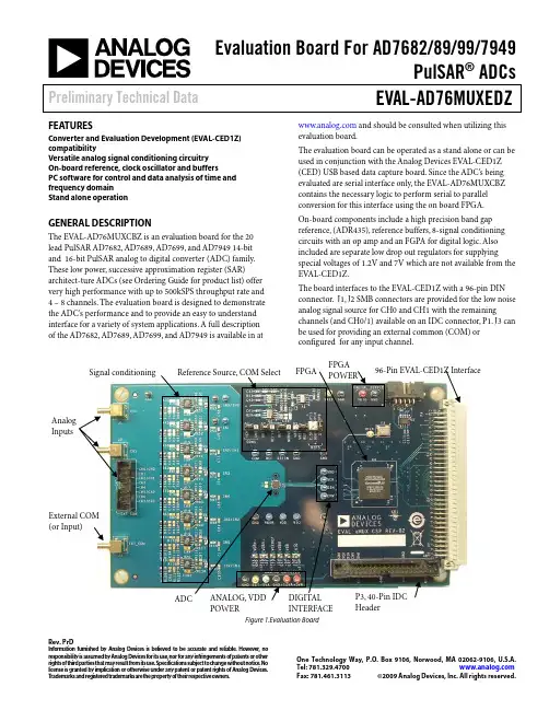
Evaluation Board For AD7682/89/99/7949PulSAR ® ADCs Preliminary Technical DataEVAL-AD76MUXEDZRev. PrDInformation furnished by Analog Devices is believed to be accurate and reliable. However , no responsibility is assumed by Analog Devices for its use, nor for any infringements of patents or other rights of third parties that may result from its use. Specifications subject to change without notice. No license is granted by implication or otherwise under any patent or patent rights of Analog Devices. T rademarks and registered trademarks are the property of their respective owners.O ne Technology Way, P.O. Box 9106, Norwood, MA 02062-9106, U.S.A.Tel: 781.329.4700 Fax: 781.461.3113 ©2009 Analog Devices, Inc. All rights reserved.FEATURESConverter and Evaluation Development (EVAL-CED1Z) compatibilityVersatile analog signal conditioning circuitry On-board reference, clock oscillator and buffersPC software for control and data analysis of time and frequency domain Stand alone operationGENERAL DESCRIPTIONThe EV AL-AD76MUXCBZ is an evaluation board for the 20 lead PulSAR AD7682, AD7689, AD7699, and AD7949 14-bit and 16-bit PulSAR analog to digital converter (ADC) family. These low power, successive approximation register (SAR)architect-ture ADCs (see Ordering Guide for product list) offer very high performance with up to 500kSPS throughput rate and 4 – 8 channels. The evaluation board is designed to demonstrate the ADC's performance and to provide an easy to understand interface for a variety of system applications. A full description of the AD7682, AD7689, AD7699, and AD7949 is available in at and should be consulted when utilizing this evaluation board.The evaluation board can be operated as a stand alone or can be used in conjunction with the Analog Devices EV AL-CED1Z (CED) USB based data capture board. Since the ADC’s being evaluated are serial interface only, the EV AL-AD76MUXCBZ contains the necessary logic to perform serial to parallel conversion for this interface using the on board FPGA. On-board components include a high precision band gapreference, (ADR435), reference buffers, 8-signal conditioning circuits with an op amp and an FGPA for digital logic. Also included are separate low drop out regulators for supplyingspecial voltages of 1.2V and 7V which are not available from the EV AL-CED1Z.The board interfaces to the EV AL-CED1Z with a 96-pin DIN connector. J1, J2 SMB connectors are provided for the low noise analog signal source for CH0 and CH1 with the remainingchannels (and CH0/1) available on an IDC connector, P1. J3 can be used for providing an external common (COM) or configured for any input channel.Figure 1.Evaluation BoardAnalog InputsSignal conditioningExternal COM (or Input)Header96-Pin EVAL-CED1Z InterfacePOWERINTERFACEEVAL-AD76MUXEDZPreliminary Technical DataRev. PrD | Page 2 of 26TABLE OF CONTENTSFeatures..............................................................................................1 Revision History...............................................................................2 Overview........................................................................................3 Conversion Control......................................................................3 Analog Inputs................................................................................3 Serial Interface..............................................................................3 Reference.......................................................................................3 Power Supplies and Grounding..................................................3 Schematics/PCB Layout...............................................................4 Hardware Setup............................................................................4 Software Installation.....................................................................4 Running the Evaluation Software..............................................5 Setup Screen...................................................................................5 Configuring the ADC...................................................................5 DC Testing - Histogram...............................................................5 AC Testing......................................................................................5 Software Operation.......................................................................8 ADC Configuration......................................................................9 Evaluation Board Schematics and Artwork............................15 Ordering Guide.. (26)LIST OF FIGURESFigure 1.Evaluation Board...............................................................1 Figure 2. Setup Screen......................................................................8 Figure 3. Default CFG.....................................................................9 Figure 4. CGF Enable/Disable Selection.......................................9 Figure 5. Input Configuration/Channel Selection........................9 Figure 6.BW Select............................................................................9 Figure 7. Reference Selection..........................................................9 Figure 8. Context Help, User Controls.........................................10 Figure 9. Histogram Screen...........................................................11 Figure 10. Summary.......................................................................12 Figure 11. FFT Spectrum...............................................................13 Figure 12 .Oscilloscope..................................................................14 Figure 13. Schematic, ADC + Block Diagram.............................15 Figure 14. Schematic, Supplies......................................................16 Figure 15. Schematic, Reference, Buffer, V CM , V BIAS ....................17 Figure 16. Schematic, AnalogCH0-CH3......................................18 Figure 17. Schematic, AnalogCH4-CH7......................................19 Figure 18. Schematic, FPGA..........................................................20 Figure 19. Schematic, 96-Pin Interface........................................21 Figure 20. Top Side Silk-Screen....................................................22 Figure 21. Inner Layer 1.................................................................22 Figure 22. Ground Plane................................................................23 Figure 23. Inner Layer 2.................................................................23 Figure 24.Inner Layer 3..................................................................24 Figure 25. Bottom Layer................................................................24 Figure 26. Bottom Layer. (25)LIST OF TABLESTable 1. Jumper Description............................................................6 Table 2.Test Points............................................................................7 Table 3. Bill of Materials for the Connectors (7)REVISION HISTORYPreliminary Technical DataEVAL-AD76MUXEDZRev. PrD | Page 3 of 26OVERVIEWFigure 1 shows the EV AL-AD76MUXCBZ evaluation board. When used in conjunction with the EV AL-CED1Z, the FPGA, U6, provides the necessary control signals for conversion and buffers the ADC serial output data into 16-bit wide transfers. The evaluation board is a flexible design that enables the user to choose among many different board configurations, analog signal conditioning, reference, and different interfaces for conversion results.In stand alone operation, the FPGA can be used to buffer the 4-wire interface via. P3, or directly to the 4 digital interface test points SDO, SCK, DIN and CNV . For stand alone mode, supply power to the evaluation board as detailed in the Power Supplies and Grounding section below.For FPGA buffered serial interface, supplying power is all that is necessary. For direct serial connection to the ADC, place a jumper across P3-39 and P3-40 as P3-40 pulled low places the FPGA into high impedance.CONVERSION CONTROLConversion start (CNV) controls the sample rate of the ADC and is the only input needed for conversion; all SAR timing is internally generated on the ADC. CNV is generated by the gate array and the frequency is selected with the software.While the ADC is converting, activity is indicated by the green LED, CR1. Operating the software in Burst mode as opposed to Continuous mode, will only light the LED when conversion is taking place.For stand alone operation, connect a low jitter source to eitherP3-8 or CNV .ANALOG INPUTSSMB connectors, J1 and J2, are provided for the ADC input channels IN0 and IN1 (IN0 only on AD7682). These inputs arealso on the IDC connector P1-2 and P1-4. The remaining inputs are also on P1-6 through P1-16 (even pins only). J3 can be configured for providing a common point (COM) for all input signals or for any analog input IN0-IN7. For using J3 as an external common point, remove the solder pad (bottom of PCB) from “COMS to COM” and solder “EXT_COM to COM” as shown below.To configure J3 to drive any of the analog input channels,remove R35 from the left pads (bottom of PCB) and solder it to the rightmost pads.The analog input amplifier circuitry U13 – U20 (see schematic - Figure 13) allows flexible configuration changes such as positive or negative gain, input range scaling, filtering, addition of a DC component, use of different op-amp and supplies. The analog input amplifiers are set as unity gain buffers at the factory. The supplies are selectable with solder pads VDRV- and VDRV+ and are set for the +7V , -5V range.Note that when using the unipolar configuration, COMS (P8) is set to (P8, 2-3) and for bipolar input configuration set to (P8, 1-2) with pin 1 being the leftmost pin.SERIAL INTERFACEThe 3-wire serial interface DIN, SCK, and SDO along with CNV are present on the digital interface test points and FPGAbuffered versions are on the 40-pin IDC connector, P3-2, -4, -6, -8. When connected to the EVAL-CED1Z and stand alone (without P3-39 to P3-40 jumper), signals are present at both locations. With P3-39 to P3-40 connected, these signals are only present at the test points SDO, SCK DIN and CNV .REFERENCEAll of the ADCs for this evaluation board can use a precision trimmed on-chip band gap reference, an on-board precision ADR435 band gap reference, or an external reference connected to the EXTREF test point (TP17). The on-chip reference is enabled or disabled with the software. The on-chip reference can be set for 2.5V or 4.096V outputs and also includes aninternal buffer, useful for external reference applications. When using the on-chip reference, remove the jumper on TP7 since this will overdrive the on-chip reference with the external one. The default configuration is for on-board ADR435 reference with a buffered output (P5 2-3), (P6 1-2) and (P7 1-2). For using an external reference connect to the EXTREF test point (TP17), select a buffer or not with P6 and select if driving the ADC REF directly or using the ADC’s internal reference buffer. When using the internal reference buffer with gain=1, the maximum output is limited to 4.096V (headroom from 5V supply).The default configuration sets the amplifiers output to be at V REF /2 (mid-scale) from the voltage divider at U1B (V BIAS ).POWER SUPPLIES AND GROUNDINGTo attain high resolution performance, the board was designed to ensure that all digital ground return paths do not cross the analog ground return paths by connecting the planes together directly under the converter. Power is supplied to the board through P3 when using with the EV AL-CED1Z. For stand aloneEVAL-AD76MUXEDZPreliminary Technical DataRev. PrD | Page 4 of 26operation, the evaluation board requires three diffeetn supplies and system ground. Connect a supply (7V to 12V) to the analog supplies tests points +12V and +5V A. Connect -5V to the -5V A test point. Connect a supply (+3.3V to +5.5V max) to the FPGA power test point, VDIG.Connect the power supply GNDs to the GND test point at the power supplies section of test points making certain the both analog and digital GNDs are at the same potential.SCHEMATICS/PCB LAYOUTThe EV AL-AD76MUXCBZ is a 6-layer board carefully laid out and tested to demonstrate the specific high accuracyperformance of the ADC. Figure 13 through Figure 19 shows the schematics of the evaluation board. The silkscreens for the PCB are given in Figure 20 and Figure 22.HARDWARE SETUPSystem Requirements• EV AL-AD7682CBZ, EV AL-AD7689CBZ, EV AL-AD7699CBZ, EV AL-AD7949CBZ• Evaluation Converter Evaluation and Development board, EV AL-CED1Z• Enclosed World compatible 7V DC supply • Enlcosed USB to mini USB cable• DC source (low noise for checking different input ranges) • AC source (low distortion)• Band pass filter suitable for 16 or 18 bit testing (value based on signal frequency)• PC operating Windows XP .Proceed to the Software Installation section to install the software. Note: The EV AL-CED1Z board must not be connected to the PC’s USB port until the Software is installed. The 7V DC supply can be connected however to check the board has power (green LED lit).SOFTWARE INSTALLATIONIt is recommended to close all Windows’ applications prior to installing the software.System Requirements• PC operating Windows XP . • USB 2.0 (for CED board) • Administrator privilegesCD-ROM –Navigate to Software\CED Version x.x, double click on setup.exe and follow the instructions on the screen. Ifanother version of Analog Devices PulSAR Evaluation Software is present, it may be necessary to remove this. To remove, click on the Windows “Start” button, select “Control Panel” and “Add or Remove Programs”. When the list populates, navigate to Analog Devices High Resolution sampling ADC’s Evaluation Software or PulSAR Evaluation Software and select Remove. Website DownloadThe software versions are also available from the Analog Devices PulSAR Analog to Digital Converter Evaluation Kitpage. After downloading the software, it is recommended to use the WinZip “Extract” function to extract all of the necessary components as opposed to just clicking on setup.exe in thezipped file. After extracting, click on seteup.exe in the folder created during the extraction and follow the instructions on the screen. If another version exists, it may be necessary to removeas detailed in the above CD-ROM section.USB DriversThe software will also install the necessary USB drivers. After installing the software, power up the CED board and connect to the PC USB 2.0 port. The Windows “Found New Hardware” Wizard will display. Click on Next to install the drivers automatically.When installed properly, Windows displays the following.On some PCs, the Found New hardware Wizard may show up again and if so follow the same procedure to install it properly. The “Device Manager” can be used to verify that the driver was installed successfully.Preliminary Technical DataEVAL-AD76MUXEDZRev. PrD | Page 5 of 26Troubleshooting the InstallIf the driver was not installed successfully the device manager will display a question mark for “Other devices” as Windows does not recognize the CED1Z board.The “USB Device” can be opened to view it’s uninstalled properties.This is usually the case if the software and drivers were installed by a user without administrator privileges. If so, log on as an administrator with full privileges and reinstall the software.RUNNING THE EVALUATION SOFTWAREThe evaluation board includes software for analyzing theAD7682, AD7689, AD7699 and AD7949. The EV AL-CED1Z is required when using the software. The software is used to perform the following tests:• Histogram for determining code transition noise (DC) • Fast Fourier transforms (FFT) for signal to noise ratio (SNR), SNR and distortion (SINAD), total harmonicdistortion (THD) and spurious free dynamic range (SFDR) • Decimation (digital filtering)The software is located at C:\Program Files\Analog Devices\ PulSAR ADC Evaluation Software\Eval PulSAR CED.exe . A shortcut is also added to the Windows “Start” menu under “Analog Devices PulSAR ADC Evaluation Software”, “Eval PulSAR CED”. To run the software, select the program from either location.SETUP SCREENFigure 2 is the setup screen where ADC device selection, test type, input voltage range, sample rate and number of samples are selected.CONFIGURING THE ADCThese ADCs need to be configured through a dedicated SPI compatible serial port. The included SW configures the part to a default configuration. Each of the different configurable parameters are shown in the ADC Configuration section, detailed in Figure 3 to Figure 7.DC TESTING - HISTOGRAMFigure 9 is the histogram screen, which tests the codedistribution for DC input and computes the mean and standard deviation or transition noise. To perform a histogram test, select “Histogram” from the test selection window and click on the “Start” radio button. Note: a histogram test can be performed without an external source since the evaluation board has a buffered V REF /2 source at the ADC input. To test other DC values, apply a source to the J1/J2/P1-x inputs. It is advised to filter the signal to make the DC source noise compatible with that of the ADC.AC TESTINGFigure 11 is the FFT screen, which performs an FFT on the captured data and computes the SNR, SINAD, THD and SFDR. Figure 12 is the time domain representation of the output. To perform an AC test, apply a sinusoidal signal to the evaluation board at the SMB inputs J1 for CH0 and J2 for CH1. Low distortion, better than 100dB, is required to allow trueevaluation of the part. One possibility is to filter the input signal from the AC source. There is no suggested bandpass filter butEVAL-AD76MUXEDZPreliminary Technical DataRev. PrD | Page 6 of 26consideration should be taken in the choice. Furthermore, if using a low frequency bandpass filter when the full-scale input range is more than a few Vpp, it is recommended to use the on board amplifiers to amplify the signal, thus preventing the filter from distorting the input signal.Table 1. Jumper DescriptionJumper Name Default Position Function P5-REFS Reference source selection.REFS to middle pin: uses ADR435 (A1) 5V, 4.096V or 2.5V output. VDD to middle pin: VDD supply is used as a reference. Open: optional source can be connected to TP17/V REF .P6 -BUF Reference buffer selection.BUF to middle pin: buffer selection from P5 with the AD8032-A (U2). NOBUFF to middle pin: use P5 direct (no buffer).P7 REF/REFINREF ADC REF/REFIN input selection.REF to middle pin: external source drives ADC REF pin.REFIN to middle pin: external source drives REFIN, reference buffer input pin Open: When using the on-chip reference.P8 COMSVCM Common channel select.VCM to middle pin: for bipolar mode, selects V REF /2. GND to middle pin: for unipolar operation, selects GND.JP9 5V 5V External reference selection of 5V. JP10 4.096V Open External reference selection of 4.096V. JP11 2.5VOpen External reference selection of 2.5V. SB0-7 BUF SelectBUF Use on-board analog amplifiers (U13 – U20)BUF: use amplifierNO BUF: bypass amplifier- VDRV- -5V Amplifiers (U13-U20) (-) supply. - VDRV+ 7V Amplifiers (U13-U20) (+) supply. - VCCREF 12V ADR435(A1) (+) supply. - VDDR 5V ADC (U7) VDD supply. Must always be the same as VDD. - VDD 5V ADC (U7) VDD supply. - VIO3.3V ADC (U7) VIO interface supply.Preliminary Technical DataEVAL-AD76MUXEDZRev. PrD | Page 7 of 26Table 2.Test PointsTest Point Available Signal Type Description TP8 GND P FPGA power supply GND. TP9 -5VA 1 P Amplifier negative supply. TP10 +5VA 1 P 5V analog supply. TP11 +12VA 1 P 12V analog supply. TP12 GND P Analog supply GND. TP13 VDD P ADC (U7) VDD supply.TP14 VDDR P ADC (U7) VDD supply. Must always be = AVDD above. TP15 VIO P ADC (U7) VIO interface supply. TP17 VREF AI External reference input.TP18 REFAI/O ADC on-chip reference output or external reference input.TP19 REFIN AI/O ADC on-chip band-gap output or external reference input when using on-chip reference buffer.TP20 IN0 AI Analog input for ADC IN0 on both 4 and 8-channel ADCs. TP21 IN1 AI Analog input for channel 1 on 8-channel ADCs only. TP22 COM AI Sets the level on ADC COM; GND or V REF /2. TP24 SDO DO Serial data output from ADC. TP25 SCK DI Serial clock data input to ADC.TP26 DIN DI Serial data input for part configuration. TP27 CNV DI Conversion input to ADC TP71 GND P Analog supply GND. TP76 VDIG 1PFPGA power supply.Table 3. Bill of Materials for the ConnectorsRef Des Connector Type Manf. Part No. J1, J2, J3 RT Angle SMB MalePasternack PE4177P1 0.100 X 0.100 straight IDC header 2X10 3M 2540-6002UB P2 0.100 X 0.100 straight IDC header 2X20 3M 2540-6002UB P432X3 RT PC MOUNT CONNECTOR ERNI 5334021Supplied by EVAL-CED1Z when connected.EVAL-AD76MUXEDZPreliminary Technical DataRev. PrD | Page 8 of 26Figure 2. Setup ScreenThe following details the operation of the software.1. The arrowis used to start the software. When runningis displayed.2.The part to be evaluated is selected here. 3. The controls are used to set:Sample Frequency – units can be used such as 500k (casesensitive) for 500,000 Hz.Capture Mode – This selects between continuous (Cont.) or burst conversion modes. In continuous mode, the ADC is continuously converting. In Burst mode, the ADC is not converting (sample clock held in inactive state) and the conversions begin once the “Single Capture ” or “Continuous Capture ” buttons have been selected.Interface mode – This selects the digital interface to the on-board FPGA.Input Range – this is used to adjust the LSB size in the data field of the plot window.4. These controls are used for saving, printing, help, etc. and are also accessed in the File menu.Save (F5): type – LabView config, allows the currentconfiguration to be saved to a filename.dat file. Useful when changing many of the default controls. To load the saved configuration, use the Load Previous Configuration. Note the location of the .dat file. It is recommended to place into the Support Files directory in the directory where the software was installed.Type – Html, saves the current screen shot to an Html file. Type – Spreadsheet, saves the current data displayed in the chart in a tab delimited spreadsheet. Raw ADC Data is time domain in V or Code, FFT or Decimated is in dB.5. Stop (F10) is used to stops the software. The can also be used to stop the software. RESET is used to reset the EVAL-CED1Z.Preliminary Technical DataEVAL-AD76MUXEDZRev. PrD | Page 9 of 26ADC CONFIGURATIONThe ADC needs to be configured for input configuration,reference, channel to be converted, temperature sensor, and on-chip low pass (LP) filter (optional) for full bandwidth (BW) or ¼ BW . These next figures show the pull down configurations available. Note the default value when the program is started isindicated by the √; or CFG writing enabled, unipolar INn to GND, CH0, full BW , and external reference. Note that after updating the CFG, the first conversion (when using burst mode) will be of the last configuration since the ADC has a 1-depp delay for the CFG. Figure 3 shows the default values.Figure 3. Default CFGFigure 4 details CFG Write Enabled/Disabled. When enabled, the MSB of the CFG is set high. When disabled the MSB is set low thus the remaining 13 bits are ignored.Figure 4. CGF Enable/Disable SelectionFigure 5 details the inputs (IN0-IN7) configuration and channelselection. Refer to the datasheet for more information about the input configure-ations. Note that in the bipolar mode, the input, IN+ and COM (or IN-) must be centered around VREF/2.Figure 5. Input Configuration/Channel SelectionFigure 6 details the bandwidth selection of the 1-pole low passfilter, which can reduce the noise from the amplifier circuit, if desired. Note that the throughout of the converter must also reduce to ¼ of the maximum when setting to ¼ BW .Figure 6.BW SelectFigure 7 details the reference selection. Note that the TEMP sensor can be used with an external reference. The Temp sensor can be used to monitor the temperature of the ADC and the output is straight binary and referenced to the ADC GND. The displayed results should be in Volts format as opposed to Hex.Figure 7. Reference SelectionEVAL-AD76MUXEDZPreliminary Technical DataRev. PrD | Page 10 of 261. To use the on-screen help. Select Help, Show Context Help or click the Help (F1). An example of the Context Help is shown above for the Sample Frequency. Placing the curser on most screen items displays useful help for the particular control or displayed unit.2. These controls are used for axes and zooming panning.Locks the graph axis to automatically fit the data. Uses last axis set by user. ,rescale the axes to theautomatic values. , are used to set axes properties such as format, precision, color, etc.Displays the cursor.Is used For zooming in and out. Is used for panning.Is used to set various graph properties such as graphtype, colors, lines, etc.Preliminary Technical DataEVAL-AD76MUXEDZRev. PrD | Page 11 of 26Figure 9. Histogram Screen1. These radio buttons are used to perform a Single Capture orContinuous Capture of data set in the # of Samples field. The results are displayed in the chart. Note that the results can be displayed as:AOr an(time domain)2., 3.These display the statistics for the X and Y-axes,respectively.EVAL-AD76MUXEDZPreliminary Technical DataRev. PrD | Page 12 of 26Figure 10. SummaryThe charts can be displayed together when the tab is selected.Rev. PrD | Page 13 of 26Figure 11. FFT Spectrum1. Displays the FFT when the Spectrum chart is selected2.,3. Display the data for the X and Y-axes, respectively.EVAL-AD76MUXEDZPreliminary Technical DataRev. PrD | Page 14 of 26Figure 12 .Oscilloscope1. Time domain data can be viewed with the oscilloscope also.Preliminary Technical Data EVAL-AD76MUXEDZ EVALUATION BOARD SCHEMATICS AND ARTWORKFigure 13. Schematic, ADC + Block DiagramRev. PrD | Page 15 of 26EVAL-AD76MUXEDZ Preliminary Technical DataRev. PrD | Page 16 of 26Preliminary Technical Data EVAL-AD76MUXEDZFigure 15. Schematic, Reference, Buffer, V CM, V BIASRev. PrD | Page 17 of 26EVAL-AD76MUXEDZ Preliminary Technical DataRev. PrD | Page 18 of 26Preliminary Technical Data EVAL-AD76MUXEDZRev. PrD | Page 19 of 26EVAL-AD76MUXEDZ Preliminary Technical DataRev. PrD | Page 20 of 26Preliminary Technical Data EVAL-AD76MUXEDZEVAL-AD76MUXEDZ Preliminary Technical DataFigure 20. Top Side Silk-Screen(Viewed from top side)Figure 21. Inner Layer 1(Viewed from top side)Preliminary Technical Data EVAL-AD76MUXEDZFigure 22. Ground Plane(Viewed from top side)Figure 23. Inner Layer 2(Viewed from top side)EVAL-AD76MUXEDZ Preliminary Technical DataFigure 24.Inner Layer 3(Viewed from top side)Figure 25. Bottom Layer(Viewed from top side)Preliminary Technical Data EVAL-AD76MUXEDZFigure 26. Bottom Layer(Viewed from Bottom Side)。