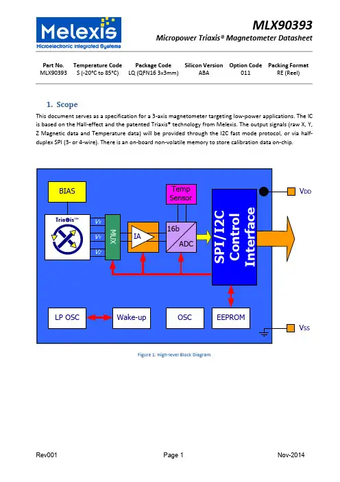
Part No. Temperature Code Package Code Silicon Version Option Code Packing Format MLX90393 S (-20°C to 85°C) LQ (QFN16 3x3mm) ABA 011 RE (Reel)1. ScopeThis document serves as a specification for a 3-axis magnetometer targeting low-power applications. The IC is based on the Hall-effect and the patented Triaxis® technology from Melexis. The output signals (raw X, Y, Z Magnetic data and Temperature data) will be provided through the I2C fast mode protocol, or via half-duplex SPI (3- or 4-wire). There is an on-board non-volatile memory to store calibration data on-chip.Figure 1: High-level Block DiagramV DDV SS2.Absolute Maximum RatingsThe MLX90393 can withstand the conditions described in the table below for short periods of time; they do not constitute conditions for normal operation.Parameter Remark Min Nom Max Unit V DD_MAX Analog Supply Voltage Limits -0.3 4 VV DD_IO_MAX Digital IO Supply Limits -0.3 min(4, V DD+0.3) V T STORAGE Storage (idle) temperature range -50 125 °C ESD HBM According to AEC-Q100-002 2.5 kV ESD CDM According to AEC-Q100-011-B (QFN) 750 V3.Thermal SpecificationThe MLX90393 has an on-board temperature sensor which measures the temperature of the MLX90393 sensor. The temperature can be read out via the communication protocol in a digital format.Parameter Remark Min Nom Max Unit T RES Temperature sensor resolution 45.2 LSB/°C T25Temperature sensor output at 25°C 46244 LSB16u T LIN Temperature Linearity(1)+/-3 °CT OPERATING Operating temperature range -20 25 85 °C(1)The linearity is defined as the best fit curve through the digital temperature outputs over the entiretemperature range. It includes ADC non-linearity effects.4.Electrical SpecificationThe specifications are applicable at 25degC, unless specified otherwise, and for the complete supply voltage range.(1)Standby current corresponds to the current consumed in the digital, where not the main oscillator isrunning which is used for analog sequencing, but only the low-power oscillator. This standby current is present in Burst mode; whenever the ASIC is counting down to start a new conversion.(2)Idle current is the current that is drawn by the ASIC in the IDLE mode, where it can only receive newcommands on the communication bus, but all other blocks are disabled. The analog (excluding the power-on-reset block) is disconnected, only the digital IO part allows clocking of a few vital gates.5.Timing SpecificationThe specifications are applicable at 25degC, unless specified otherwise, and for the complete supply voltage range.(1)This conversion time is defined as the time to acquire a single axis of the magnetic flux density.When measuring multiple axes, they are obtained through time-multiplexing, i.e. X(t), Y(t+T CONVM) and Z(t+2*T CONVM). The conversion time is programmable through parameters OSR and DIG_FILT for magnetic conversion time and OSR2 for temperature conversion time. The conversion sequence is always TXYZ, the opposite of the ZYXT argument of the command set.(2)The time T INTERVAL is defined as the time between the end of one set of measurements (anycombination of TXYZ) and the start of the following same set of measurements in BURST and WOC mode. As a result of this, the maximum output data rate is not only a function of T INTERVAL but equals 1/(T CONV_BURSTWOC + T INTERVAL).(3)6.Magnetic SpecificationThe specifications are applicable at 25degC, unless specified otherwise, and for the complete supply voltage range.(1)The offset thermal drift is defined as the deviation at 0Gauss from the output with respect to theoutput at 25°C when sweeping the temperature. The highest gradient (µT/°C) typically occurs at 85°C. The spec value is based on characterization on limited sample size at GAIN_SEL=0x7 and RES_XYZ=0x00.(2)The total axis sensitivity is programmable to support different applications, but has no AutomaticGain control on-chip as do the other angular position sensors from Melexis. The highest gain corresponds to at least the minimum +/-4.8mT magnetic measurement range and the magnetic resolution defined by SENS ii.(3)The sensitivity thermal drift is expressed as a band around the sensitivity at 25°C. It is applicable onwafer level trimming, but can be influenced by packaging (overmolding).,RES Z} X YFigure 2: XY axis RMS noise versus conversion time, expressed in mGauss for GAIN_SEL = 0x7Figure 3: Z axis RMS noise versus conversion time, expressed in mGauss for GAIN_SEL = 0x77.Functional SpecificationThe MLX90393 can operate in 3 modes:∙Burst mode: The ASIC will have a programmable data rate at which it willoperate. This data rate implies auto-wakeup and sequencing of the ASIC,flagging that data is ready on a dedicated pin (INT/DRDY). The maximumdata rate corresponds to continuous burst mode, and is a function of thechosen measurement axes. For non-continuous burst modes, the timeduring which the ASIC has a counter running but is not doing an actualconversion is called the Standby mode (STBY).∙Single Measure mode: The master will ask for data via the correspondingprotocol (I2C or SPI), waking up the ASIC to make a single conversion,immediately followed by an automatic return to sleep mode (IDLE) until thenext polling of the master. This polling can also be done by strobing the TRGpin instead, which has the same effect as sending a protocol command for asingle measurement.∙Wake-Up on Change: This mode is similar to the burst mode in the sensethat the device will be auto-sequencing, with the difference that themeasured component(s) is/are compared with a reference and in case thedifference is bigger than a user-defined threshold, the DRDY signal is set onthe designated pin. The user can select which axes and/or temperature fallunder this cyclic check, and which thresholds are allowed.The user can change the operating mode at all time through a specific command on the bus. The device waits in IDLE mode after power-up, but with a proper user command any mode can be set after power-up. Changing to Burst or WOC mode, coming from Single Measure mode, is always accompanied by a measurement first. The top-level state diagram indicating the different modes and some relevant timing is shown below in Figure 4. In the Measure state, the MDATA flag will define which components will be measured (ZYXT). The order of conversion is defined as TXYZ and can not be modified by the user, only the combination of axes is a degree of freedom.Arrows indicated in grey are the direct result of an Exit command. The main difference between STANDBY and WOC_IDLE is that in STANDBY mode, all analog circuitry is ready to make a conversion, but this is accompanied by a larger current consumption than IDLE mode. For burst mode this extra current consumption is justified because the emphasis is more on accurate timing intervals, avoiding the delay of T STBY before conversion and supporting an efficient continuous burst mode without standby overhead.It is the user’s responsibi lity to read back the measured data, the MLX90393 acts as a pure slave. Even in burst mode and WOC mode when the MLX90393 is auto-sequencing, the master will be responsible for collecting the acquired sensor data.TIMEm*T CONVM + T CONVTT ACTIVET STBYT PORFigure 4: Top-level state diagram with indication of timings7.1 Burst modeWhen the sensor is operating in burst mode, it will make conversions at specific time intervals. The programmability of the user is the following:∙ Burst speed (T INTERVAL ) through parameter BURST_DATA_RATE ∙ Conversion time (T CONV ) through parameters OSR, OSR2 and DIG_FILT∙ Axes/Temperature (MDATA) through parameter BURST_SEL or via the command argument (ZYXT)Whenever the MLX90393 has made the selected conversions (based on MDATA), the DRDY signal will be set (active H) on the INT and/or INT/TRG pin to indicate that the data is ready for readback. It will remain high until the master has sent the command to read out at least one of the converted quantities (ZYXT). Should the master have failed to read out any of them by the time the sensor has made a new conversion, the INT/DRDY pin will be strobed low for 10us, and the next rising edge will indicate a new set of data is ready.7.2 Single Measurement modeWhenever the sensor is set to this mode (or after startup) the MLX90393 goes to the IDLE state where it awaits a command from the master to perform a certain acquisition. The duration of the acquisition will be the concatenation of the T STBY, T ACTIVE, m*T CONVM(with m # of axes) and T CONVT. The conversion time will effectively be programmable by the user (see burst mode), but is equally a function of the required axes/temperature to be measured.Upon reception of such a polling command from the master, the sensor will make the necessary acquisitions, and set the DRDY signal high to flag that the measurement has been performed and the master can read out the data on the bus at his convenience. The INT/DRDY will be cleared either when:∙The master has issued a command to read out at least one of the measured components∙The master issues an Exit (EX) command to cancel the measurement∙The chip is reset, after POR (Power-on reset) or Reset command (RT)7.3Wake-Up on Change modeThe Wake-Up on Change (WOC) functionality can be set by the master with as main purpose to only receive an interrupt when a certain threshold is crossed. The WOC mode will always compare a new burst value with a reference value in order to assess if the difference between both exceeds a user-defined threshold. The reference value is defined as one of the following:∙The first measurement of WOC mode is stored as reference value once, as a result of a measurement. This measurement at “t=0” is then the basis for comparison or,∙The reference for acquisition(t) is always acquisition(t-1), in such a way that the INT signal will only be set if the derivative of any component exceeds a threshold.∙The in-application programmability is the same as for burst mode, but now the thresholds for setting the interrupt are also programmable by the user, as well as the reference, if the latter is data(t=0) or data(t-1).8.Digital SpecificationThe supported protocols are I2C and SPI. The SENB/CS pin is used to define the protocol to be used:∙/CS = 0 for SPI, addressing the MLX90393 slave in SPI mode (3- and 4-wire), but releasing this line in between commands (no permanent addressing allowed)∙/CS = 1 for I2C, addressing the MLX90393 slave when the correct address is transmitted over the bus (permanently kept high)To make sure the activity on the SPI bus can not be accidentally interpreted as I2C protocol, programming bits are available in the memory of the MLX90393 to force the communication mode. It concerns the COMM_MODE[1:0] bits with the following effect:8.1Command ListThe MLX90393 only listens to a specific set of commands. Apart from the Reset command, all commands generate a status byte that can be read out. The table below indicates the 10 different commands that are (conditionally) accepted by the MLX90393. The MLX90393 will always acknowledge a command in I2C, even if the command is not a valid command. Interpreting the associated status byte is the method for verification of command acceptance.The argument for the volatile memory access commands (RR/WR) «abc» should be set to 0x0h, in order to get normal read-out and write of the memory.The argument in all mode-starting commands (SB/SW/SM) is a nibble specifying the conversions to be performed by the sensor in the following order «zyxt». For example, if only Y axis and temperature are to be measured in Single Measurement mode the correct command to be transmitted is 0x35h. The sequence of measurement execution on-chip is inverted to «TXYZ», so T will be measured before X, followed by Y and finally Z. By issuing an all-zero «zyxt» nibble, the BURST_SEL value from RAM will be used instead of the empty argument of the command.8.2Status ByteThe status byte is the first byte transmitted by the MLX90393 in response to a command issued by the master. It is composed of a fixed combination of informative bits:∙MODE bitsthese bits define in which mode the MLX90393 is currently set. Whenever a mode transition command is rejected, the first status byte after this command will have the expected mode bit cleared, which serves as an indication that the command has been rejected, next to the ERROR bit. The SM_MODE flag can be the result of an SM command or from raising the TRG pin when TRG mode is enabled in the volatile memory of the MLX90393.∙ERROR bitthis bit is set in case a command has been rejected or in case an uncorrectable error is detected in the memory, a so called ECC_ERROR. A single error in the memory can be corrected (see SED bit), two errors can be detected and will generate the ECC_ERROR. In such a case all commands but the RT (Reset) command will be rejected. The error bit is equally set when the master is reading back data while the DRDY flag is low.∙SED bitthe single error detection bit simply flags that a bit error in the non-volatile memory has been corrected. It is purely informative and has no impact on the operation of the MLX90393.∙RS bitwhenever the MLX90393 gets out of a reset situation –both hard and soft reset –the RS flag is set to highlight this situation to the master in the first status byte that is read out. As soon as the first status byte is read, the flag is cleared until the next reset occurs.D[1:0] bitsthese bits only have a meaning after the RR and RM commands, when data is expected as a response from the MLX90393. The number of response bytes correspond to 2*D[1:0] + 2, so the expected byte counts are either 2, 4, 6 or 8. For commands where no response is expected, the content of D[1:0] should be ignored.8.3SPI CommunicationThe MLX90393 can handle SPI communication at a bitrate of 10Mhz. The SPI communication is implemented in a half-duplex way, showing high similarities with I2C communication, but addressing through the \CS (Chip Select) pin instead of through bus arbitration. The half-duplex nature is at the basis of the supported 3-wire SPI operation. SPI mode 3 is implemented: CPHA=1 (data changed on leading edge and captured on trailing edge, and CPOL=1 (high level is inactive state). The Chip Select line is active-low.The communication is also bundled in bytes, equally MSB first and MSByte first. A command can of course consist of more than 1 byte (refer to Chapter 8.1) as can the response be from the MLX90393 in the form of multiple bytes after the status byte (not shown in Figure 5)COMMAND[7:0]SCL MOSI 1234567812345678MISO/CS STATUS_BYTE[7:0]X (4-wire SPI) or Z (3-wire SPI)Z (3 & 4-wire SPI)ADDNADDFigure 5: SPI communication example8.4 I 2C CommuncationI 2C AddressThe I 2C address is made up of some hard-coded bits and a memory written value as follows:I2C_ADDR[6:0] = {EE_I2C_ADDR[4:0],A 1,A 0} with A i the user-selectable active-high value of the input pads of the MLX90393, referred to the V DD supply system and EE_I2C_ADDR[4:0] default programmed to 03h, but user accessible for overwrite.I 2C PrincipleThe MLX90393 supports I 2C communication in both Standard Mode and Fast Mode. Bytes are transmitted MSB first, and in order to reconstruct words, the bytes need to be concatenated MSByte first. The general principle of communication is always the same:∙ Initiating the communication is always done by the Master (Start condition S)∙ Addressing the Slave (MLX90393) followed by a cleared bit to indicate the Master intends to writesomething to the specific addressed Slave ∙ Acknowledging by the Slave if the transmitted address corresponds to the Slave’s I 2C address. If thelatter isn’t the case, any further activity on the bus except a Sr (Start Repeat) and P (Stop) condition will be ignored by the MLX90393 ∙ Sending a Command Byte by the Master, as depicted in Figure 6. The Slave will always acknowledgethis, even if it is an unrecognized command. A command such as WR and RR consist of more than 1 byte, which can then be transmitted sequentially over the I 2C bus. Referring to Figure 6 the COMMAND byte should then be a sequence of C OMMAND byte1, byte2, etc… ∙ Issuing a Start Repeat (Sr) condition by the Master in order to restart the addressing phase∙Addressing the Slave (MLX90393) followed by a set bit to indicate the Master intends to read something from the specific addressed Slave∙Acknowledging by the Slave if the transmitted address corresponds to the Slave’s I2C address. If the latter isn’t the case, any further activity on the bus except a Sr (Start Repeat) and P (Stop) condition will be ignored by the MLX90393∙Transmitting the Status Byte by the Slave, who is in control of the bus. Following the RR and RM commands the sensor returns additional data bytes after the status byte.∙Acknowledging by the Master if the data is well received∙Generating a Stop condition (P) by the masterThe Master controlled bus activity is shown in blue, the Slave controlled bus activity is shown in orange. In case a command is longer than a single byte (see Table 6), the bytes are transmitted sequentially before generating the Start Repeat (Sr) condition.I2C_ADDR[6:0]W ACKSCOMMAND[7:0]ACKI2C_ADDR[6:0]R ACK Sr STATUS_BYTE[7:0]ACKSCL SDA SCL SDA 123456789123456789123456789P 123456789Figure 6: Default I2C communication example with status byte readbackThe same applies to the Slave responses: following RR and RM commands, the Slave response is more than just the Status Byte. There as well, the data is partitioned in bytes that are transmitted sequentially by the slave. It is the Master’s responsibility to issue enough clocking p ulses to read back all the data. Finding out how many bytes is possible by decoding the Status Byte information, see Section Status Byte.Finally the master is also free to not read back the status byte when issuing a command. In doing so, he loses the ability to see if the command was received properly by the MLX90393. Moreover, the first SM command issued by the master after power-up or reset should have the status byte read back in order to get valid measurement data back.9. Memory MapThe MLX90393 has 1kbit of non-volatile memory, and the same amount of volatile memory. Each memory consists out of 64 addresses containing 16 bit words. The non-volatile memory has automatic 2-bit error detection and 1-bit error correction capabilities per address. The handling of such corrections & detections is explained in Section Status Byte. The memory is split in 2 areas:∙ Customer area [address 0x00h to 0x1Fh] ∙ Melexis area [address 0x20h to 0x3Fh]The RR and WR commands impact the volatile memory only, there no direct access possible to the non-volatile memory. The customer area of the volatile memory is bidirectionally accessible to the customer; the Melexis area is write-protected. Only modifications in the blue area are allowed with the WR command. The adjustments in the customer area can be stored in the permanent non-volatile memory with the STORE command HS, which copies the entire volatile memory including the Melexis area to the non-volatile one. With the HR command the non-volatile memory content can be recalled to the volatile memory, which can restore any modifications due to prior WR commands. The HR step is performed automatically at start-up of the ASIC, either through cold reset or warm reset with the RT command. The above is graphically shown in Figure 7.Figure 7: The memories of the MLX90393, their areas and the impacting commands.The customer area houses 3 types of data:∙Analog configuration bits∙Digital configuration bits∙Informative (free) bitsThe latter can be filled with customer content freely, and covers the address span from (and including) 0x0Ah to 0x1Fh, a total of 352 bits. The memory mapping of volatile and non-volatile memory on address level is identical. The volatile memory map is given in Figure 8.Figure 8: Customer area memory map.The non-volatile memory can only be written (HS store command) if pin VDD is supplied with 3.3V minimum, otherwise the write sequence can not be performed in a reliable way. Additionally, this HS command was designed to be used as one-time calibration, but not as multi write-cycle memory within the application. In case memory is written within the application, the number of write cycles should be kept to a minimum. There is no limit to the write cycles in the volatile memory (WR write command).9.1Parameter DescriptionThe meaning of each customer accessible parameter is explained in this section. The customer area of both the volatile and the non-volatile memory can be written through standard SPI and I2C communication, within the application. No external high-voltages are needed to perform such operations, nor access to dedicated pins that need to be grounded in the application.ANA_RESERVED_LOW : Reserved IO trimming bitsBIST : Enabled the on-chip coil, applying a Z-field [Built-In Self Test]Z_SERIES : Enable all plates for Z-measurementGAIN_SEL[2:0] : Analog chain gain setting, factor 5 between min and max code HALLCONF[3:0] : Hall plate spinning rate adjustmentTRIG_INT_SEL : Puts TRIG_INT pin in TRIG mode when cleared, INT mode otherwise COMM_MODE[1:0] : Allow only SPI [10b], only I2C [11b] or both [0Xb] according to CS pin WOC_DIFF : Sets the Wake-up On Change based on Δ{sample(t),sample(t-1)} EXT_TRIG : Allows external trigger inputs when set, if TRIG_INT_SEL = 0 TCMP_EN : Enables on-chip sensitivity drift compensationBURST_SEL[3:0] : Defines the MDATA in burst mode if SB command argument = 0 BURST_DATARATE[6:0] : Defines T INTERVAL as BURST_DATA_RATE * 20msOSR2[1:0] : Temperature sensor ADC oversampling ratioRES_XYZ[5:0] : Selects the desired 16-bit output value from the 19-bit ADCDIG_FILT[1:0] : Digital filter applicable to ADCOSR[1:0] : Magnetic sensor ADC oversampling ratioSENS_TC_HT[7:0] : Sensitivity drift compensation factor for T < T REFSENS_TC_LT[7:0] : Sensitivity drift compensation factor for T > T REFOFFSET_i[15:0] : Constant offset correction, independent for i = X, Y, ZWOi_THRESHOLD[15:0] : Wake-up On Change threshold, independent for i = X, Y, Z and T10.Packaging Specification10.1QFN packageThe MLX90393 shall be delivered in a QFN package as shown below in Figure 9.XZYFigure 9: Package Outline DrawingThe sensing elements – Hall plates with the patented IMC technology – are located in the center of the die, which on its turn is located in the center of the package. The pinout (in name and function) is given in Table 7 below.11.Standard information regarding manufacturability of Melexisproducts with different soldering processesOur products are classified and qualified regarding soldering technology, solderability and moisture sensitivity level according to following test methods:Reflow Soldering SMD’s (Surface Mount Devices)IPC/JEDEC J-STD-020Moisture/Reflow Sensitivity Classification for Nonhermetic Solid State Surface Mount Devices (classification reflow profiles according to table 5-2)∙EIA/JEDEC JESD22-A113Preconditioning of Nonhermetic Surface Mount Devices Prior to Reliability Testing (reflow profiles according to table 2)Wave Soldering SMD’s (Surface Mount D evices) and THD’s (Through Hole Devices)∙EN60749-20Resistance of plastic- encapsulated SMD’s to combined effect of moisture and soldering heat∙EIA/JEDEC JESD22-B106 and EN60749-15Resistance to soldering temperature for through-hole mounted devicesIron Soldering THD’s (Through Hole Devices)∙EN60749-15Resistance to soldering temperature for through-hole mounted devicesSolderability SMD’s (Surface Mount D evices) and THD’s (Through Hole Devices)∙EIA/JEDEC JESD22-B102 and EN60749-21SolderabilityFor all soldering technologies deviating from above mentioned standard conditions (regarding peak temperature, temperature gradient, temperature profile etc) additional classification and qualification tests have to be agreed upon with Melexis. The application of Wave Soldering for SMD’s is allowed only after consulting Melexis regarding assurance of adhesive strength between device and board.Melexis recommends reviewing on our web site the General Guidelines soldering recommendation (/Quality_soldering.aspx) as well as trim&form recommendations (/Assets/Trim-and-form-recommendations-5565.aspx).Melexis is contributing to global environmental conservation by promoting lead free solutions. For more information on qualifications of RoHS compliant products (RoHS = European directive on the Restriction Of the use of certain Hazardous Substances) please visit the quality page on our website: /quality.aspx12.ESD PrecautionsElectronic semiconductor products are sensitive to Electro Static Discharge (ESD). Always observe Electro Static Discharge control procedures whenever handling semiconductor products.13.Recommended Application Diagram13.1I2CA1A0 I2C Address13.2SPI14.Table of Contents1.Scope (1)2.Absolute Maximum Ratings (2)3.Thermal Specification (2)4.Electrical Specification (2)5.Timing Specification (3)6.Magnetic Specification (6)7.Functional Specification (9)7.1Burst mode (11)7.2Single Measurement mode (12)7.3Wake-Up on Change mode (12)8.Digital Specification (13)8.1Command List (13)8.2Status Byte (14)8.3SPI Communication (15)8.4I2C Communcation (16)I2C Address (16)I2C Principle (16)9.Memory Map (19)9.1Parameter Description (20)10.Packaging Specification (22)10.1QFN package (22)11.Standard information regarding manufacturability of Melexis products with different soldering processes (23)12.ESD Precautions (24)13.Recommended Application Diagram (25)13.1I2C (25)13.2SPI (25)。