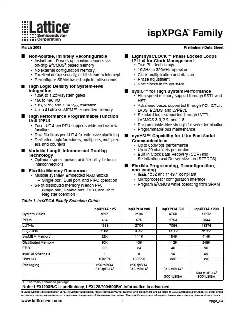
ispXPGA FamilyMarch 2003Preliminary Data SheetTM© 2003 Lattice Semiconductor Corp. All Lattice trademarks, registered trademarks, patents, and disclaimers are as listed at /legal. All other brand or product names are trademarks or registered trademarks of their respective holders. The speci fications and information herein are subject to change without notice.■Non-volatile, In finitely Recon figurable•Instant-on - Powers up in microseconds via on-chip E 2CMOS ® based memory •No external con figuration memory•Excellent design security , no bit stream to intercept •Recon figure SRAM based logic in milliseconds■High Logic Density for System-levelIntegration•139K to 1.25M system gates •160 to 496 I/O•1.8V , 2.5V , and 3.3V V CC operation•Up to 414Kb sysMEM™ embedded memory■High Performance Programmable FunctionUnit (PFU)•Four LUT -4 per PFU supports wide and narrow functions•Dual flip-flops per LUT -4 for extensive pipelining •Dedicated logic for adders, multipliers, multiplex-ers, and counters■Variable-Length Interconnect RoutingTechnology•Optimum speed, power, and flexibility for logic interconnections■ Flexible Memory Resources•Multiple sysMEM Embedded RAM Blocks–Single port, Dual port, and FIFO operation •64-bit distributed memory in each PFU–Single port, Double port, FIFO, and Shift Register operation■ Eight sysCLOCK™ Phase Locked Loops(PLLs) for Clock Management•T rue PLL technology•10MHz to 320MHz operation •Clock multiplication and division •Phase adjustment•Shift clocks in 250ps steps■ sysIO™ for High System Performance•High speed memory support through SSTL and HSTL•Advanced buses supported through PCI, GTL+, LVDS, BLVDS, and LVPECL•Standard logic supported through LVTTL, LVCMOS 3.3, 2.5, and 1.8•Programmable drive strength for series termination •Programmable bus maintenance■ sysHSI™ Capability for Ultra Fast SerialCommunications•Up to 850Mbps performance •Up to 20 channels per device•Built in Clock Data Recovery (CDR) and Serialization and De-serialization (SERDES)■ Flexible Programming, Recon figuration,and Testing•IEEE 1532 and 1149.1 compliant•Microprocessor con figuration interface•Program E 2 CMOS while operating from SRAMTable 1. ispXPGA Family Selection GuideispXPGA 125ispXPGA 200ispXPGA 500ispXPGA 1200System Gates 139K 210K 476K 1.25M PFUs 48467617643844LUT -4s 19362704705615376Logic FFs 3.8K 5.4K 14.1K 30.7K sysMEM Memory 92K 111K 184K 414K Distributed Memory 30K 43K 112K 246K EBR20244090sysHSI Channels 481220User I/O 160/176160/208336496Packaging256 fpBGA 516 fpBGA 1256 fpBGA 516 fpBGA 1516 fpBGA 1 900 fpBGA680 fpSBGA 1 900 fpBGA1.Thermally enhanced package.Note: LFX1200B/C is preliminary, LFX125/200/500B/C information is advanced.Lattice Semiconductor ispXPGA Family Data SheetispXPGA Family OverviewThe ispXPGA family of devices allows the creation of high-performance logic designs that are both non-volatile andinfinitely re-programmable. Other FPGA solutions force a compromise being either re-programmable or non-vola-tile. This family couples this capability with a mainstream architecture containing the features required for today’ssystem-level design.Electrically Erasable CMOS (E2CMOS) memory cells provide the ispXPGA family with non-volatile capability.These allow logic to be functional microseconds after power is applied, allowing easy interfacing in many applica-tions. This capability also means that expensive external configuration memories are not required and that designs can be secured from unauthorized read back. Internal SRAM cells allow the device to be infinitely reconfigured if desired. Both the SRAM and E2CMOS cells can be programmed and verified through the IEEE 1532 industry stan-dard. Additionally, the SRAM cells can be configured and read-back through the sysCONFIG™ peripheral port.The family spans the density and I/O range required for the majority of today’s logic designs, 139K to 1.25M systemgates and 160 to 496 I/O. The devices are available for operation from 1.8V, 2.5V, and 3.3V power supplies, provid-ing easy integration into the overall system.The system-level needs of designers are met through the incorporation of sysMEM dual-port memory blocks,sysIO advanced I/O support, and sysCLOCK Phase Locked Loops (PLLs). High-speed serial communications aresupported through multiple sysHSI blocks, which provide clock data recovery (CDR) and serialization/de-serializa-tion (SERDES).The ispLEVER™ design tool from Lattice allows designers easy implementation of designs using the ispXPGAproduct. Synthesis library support is available for the major logic synthesis tools. The ispLEVER tool takes the out-put from these common synthesis packages and place and routes the design in the ispXPGA product. The toolallows floor planning and the management of other constraints within the device. The tool also provides outputs tocommon timing analysis tools for timing analysis.T o increase designer productivity, Lattice provides a variety of pre-designed modules referred to as IP cores for theispXPGA product. These IP cores allow designers to concentrate on the unique portions of their design while usingpre-designed block to implement standard functions such as bus-interfaces, standard communication-interfaces,and memory-controllers.Through the use of advanced technology and innovative architecture the ispXPGA FPGA devices provide design-ers with excellent speed performance. Although design dependent, many typical designs can run at over 150MHz.Certain designs can run at over 300MHz. T able 2 details the performance of several building blocks commonlyused by logic designers.Table 2. ispXPGA Speed Performance for Typical Building BlocksFunction Performance8:1 Asynch MUX150 MHz1:32 Asynch Demultiplexer125 MHz8 x 8 2-LL Piped Multiplier225 MHz32-bit Up/Down Counter290 MHz32-bit Shift Register360 MHzLattice Semiconductor ispXPGA Family Data SheetArchitecture OverviewThe ispXPGA architecture is a symmetrical architecture consisting of an array of Programmable Function Units(PFUs) enclosed by Input Output Groups (PICs) with columns of sysMEM Embedded Block RAMs (EBRs) distrib-uted throughout the array. Figure 1 illustrates the ispXPGA architecture. Each PIC has two corresponding sysIOblocks, each of which includes one input and output buffer. On two sides of the device, between the PICs and thesysIO blocks, there are sysHSI High-Speed Interface blocks. The symmetrical architecture allows designers to eas-ily implement their designs, since any logic function can be placed in any section of the device.The PFUs contain the basic building blocks to create logic, memory, arithmetic, and register functions. They areoptimized for speed and flexibility allowing complex designs to be implemented quickly and efficiently.The PICs interface the PFUs and EBRs to the external pins of the device. They allow the signals to be registeredquickly to minimize setup times for high-speed designs. They also allow connections directly to the different logicelements for fast access to combinatorial functions.The sysMEM EBRs are large, fast memory elements that can be configured as RAM, ROM, FIFO, and other stor-age types. They are designed to facilitate both single and dual-port memory for high-speed applications.These three components of the architecture are interconnected via a high-speed, flexible routing array. The routing array consists of Variable Length Interconnect (VLI) lines between the PICs, PFUs, and EBRs. There is additionalrouting available to the PFU for feedback and direct routing of signals to adjacent PFUs or PICs.The sysIO blocks consist of configurable input and output buffers connected directly to the PICs. These buffers canbe configured to interface with 16 different I/O standards. This allows ispXPGA to interface with other devices with-out the need for external transceivers.The sysHSI blocks provide the necessary components to allow the ispXPGA device to transfer data at up to850Mbps using the LVDS standard. These components include serializing, de-serializing, and clock data recovery(CDR) logic.The sysCLOCK blocks provide clock multiplication/division, clock distribution, delay compensation, and increasedperformance through the use of PLL circuitry that manipulates the global clocks. There is one sysCLOCK block foreach global clock tree in the device.Lattice Semiconductor ispXPGA Family Data SheetLattice Semiconductor ispXPGA Family Data SheetLattice Semiconductor ispXPGA Family Data SheetLattice Semiconductor ispXPGA Family Data SheetLattice Semiconductor ispXPGA Family Data SheetLattice Semiconductor ispXPGA Family Data SheetLattice Semiconductor ispXPGA Family Data SheetLattice Semiconductor ispXPGA Family Data SheetLattice Semiconductor ispXPGA Family Data SheetLattice Semiconductor ispXPGA Family Data SheetLattice Semiconductor ispXPGA Family Data SheetLattice Semiconductor ispXPGA Family Data SheetLattice Semiconductor ispXPGA Family Data SheetLattice SemiconductorispXPGA Family Data SheetTable 5. ispXPGA Supported I/O StandardsTable 6. Differential Interface Standard Support 1sysIO StandardV CCO V REF V TT LVTTL 3.3V N/A N/A LVCMOS-3.3 3.3V N/A N/A LVCMOS-2.5 2.5V N/A N/A LVCMOS-1.8 1.8V N/A N/A PCI 3.3V N/A N/A AGP-1X3.3V N/A N/A SSTL3, Class I, II 3.3V 1.5V 1.5V SSTL2, Class I, II 2.5V 1.25V 1.25V HSTL, Class I 1.5V 0.75V 0.75V HSTL, Class III 1.5V 0.9V 1.5V GTL+N/A 1.0V 1.5V LVPECL 3.3V N/A N/A LVDS 1 2.5V N/A N/A BLVDS2.5VN/AN/A1.V CCO must be2.5V for high speed serial operations (sysHSI block).sysIO Buffer Not Using sysHSI BlocksysIO Buffer Using sysHSI Block LVDS Driver Supported with external resistor network SupportedReceiver Supported with standard termination Supported with standard termination BLVDS Driver Supported with external resistor network Not supportedReceiver Supported (may need termination)Supported (may need termination)LVPECLDriver Supported with external resistor network Not supportedReceiverSupported with terminationSupported with termination1.For more information, refer to Lattice technical note TN1000, sysIO Usage Guidelines,available at .Lattice Semiconductor ispXPGA Family Data SheetTable 7. sysHSI Block REFCLK Selections1sysHSI Block Available Global Clock Nets0CLK0, CLK1, CLK2, CLK31CLK0, CLK1, CLK2, CLK42CLK0, CLK1, CLK2, CLK53CLK0, CLK1, CLK3, CLK64CLK0, CLK1, CLK3, CLK75CLK0, CLK3, CLK5, CLK76CLK0, CLK2, CLK5, CLK77CLK0, CLK1, CLK5, CLK68CLK0, CLK5, CLK69CLK0, CLK5, CLK6, CLK71.T able 6 applies to all devices. Ignore sysHSI blocks not availablein a specific device.Configuration and ProgrammingThe ispXPGA family of devices takes a unique approach to FPGA configuration memory. It contains two types of memory, Static RAM and non-volatile E2CMOS cells. The static RAM is used to control the functionality of the device during normal operation and the E2CMOS memory cells are used to load the SRAM. The E2CMOS memory module can be thought of as the hard drive for the ispXPGA configuration and the SRAM as the working configura-tion memory. There is a one-to-one relationship between SRAM memory and the E2CMOS cells. The SRAM can be configured either from the E2CMOS memory or from an external source, as shown in Figure 21.Figure 21 shows the different ports and modes that are used in the configuration and programming of the ispXPGA devices. There are two possible ports that can be used for configuration of the SRAM memory: the ISP port which is compliant to the IEEE 1149.1 T est Access Port (T AP) Std. and the ISP port which accommodates bit-wide config-uration. The sysCONFIG port allows byte-wide configuration of the SRAM configuration memory. When program-ming the E2CMOS memory, only the 1149.1 T AP can be used.Configuration and programming done through the 1149.1 T est Access Port (T AP) are fully compliant to both the IEEE Std. 1149.1 Boundary Scan T AP specification and the IEEE Std. 1532 In-System Configuration specification. T o configure or program the device using the 1149.1 T AP the device must be in the ISP mode. T o configure the SRAM memory using the sysCONFIG Port, the device must be in the sysCONFIG mode. Upon power-up, the device’s SRAM memory can be configured either from the E2CMOS memory or from an external source through the sysCONFIG mode. Additionally, the SRAM can be re-configured from the E2CMOS memory by executing a “REFRESH.” See Lattice technical note number TN1026, is pXP Configuration Us age Guide, for more in depth information on the different programming modes, timing and wake-up, available at .Absolute Maximum Ratings 1, 2, 31.8V2.5V/3.3VSupply Voltage (V CC ). . . . . . . . . . . . . . . . . . . . . . -0.5 to 2.5V . . . . . . . . . .-0.5 to 5.5V PLL Supply Voltage (V CCP ) . . . . . . . . . . . . . . . . . -0.5 to 2.5V . . . . . . . . . .-0.5 to 5.5V Output Supply Voltage (V CCO ). . . . . . . . . . . . . . . -0.5 to 4.5V . . . . . . . . . .-0.5 to 4.5V IEEE 1149.1 T AP Supply Voltage (V CCJ ). . . . . . . -0.5 to 4.5V . . . . . . . . . .-0.5 to 4.5V Input Voltage Applied 4 . . . . . . . . . . . . . . . . . . . . . -0.5 to 4.5V . . . . . . . . . .-0.5 to 4.5V Storage T emperature . . . . . . . . . . . . . . . . . . . . . .-65 to 150°C. . . . . . . . . -65 to 150°C Junction T emperature (T J ) with Power Applied . .-55 to 150°C. . . . . . . . . -55 to 150°C1. Stress above those listed under the “Absolute Maximum Ratings” may cause permanent damage to the device. Functional operation of the device at these or any other conditions above those indicated in the operational sections of this speci fication is not implied (while programming, following the programming speci fications).2. Compliance with the Lattice Thermal Management technical note is required.3. All voltages referenced to GND.4. Overshoot and undershoot of -2V to (V IH (MAX) + 2) volts is permitted for a duration of <20nsRecommended Operating ConditionsE 2CMOS Erase Reprogram Speci ficationsHot Socketing Characteristics 1, 2, 3, 4SymbolParameterMin Max Units V CCSupply Voltage for 1.8V device1.65 1.95V Supply Voltage for2.5V device 2.3 2.7V Supply Voltage for3.3V device3.0 3.6V V CCPSupply Voltage for PLL block for 1.8V device1.65 1.95V Supply Voltage for PLL block for2.5V device 2.3 2.7V Supply Voltage for PLL block for3.3V device3.0 3.6V V CCJ Supply Voltage for IEEE 1149.1 T est Access Port for LVCMOS 1.8V1.65 1.95V Supply Voltage for IEEE 1149.1 T est Access Port for LVCMOS2.5V 2.3 2.7V Supply Voltage for IEEE 1149.1 T est Access Port for LVCMOS3.3V 3.0 3.6V T J (COM)Junction T emperature Commercial Operation 085C T J (IND)Junction T emperature Industrial Operation-40105CParameterMin Max Units Erase/Reprogram Cycle 11,000—Cycles1.Valid over commercial temperature range.Symbol ParameterConditionMin Typ Max Units I DKInput or I/O Leakage Current0 ≤ V IN ≤ 3.0V—+/-50+/-800µA1. Insensitive to sequence of V CC and V CCO . However, assumes monotonic rise / fall rates for V CC and V CCO .2. LVTTL, LVCMOS only3. 0 < V CC ≤ V CC (MAX), 0 < V CCO ≤ V CCO (MAX)4.I DK is additive to I PU , I PD or I BH . Device defaults to pull-up until fuse circuitry is active.DC Electrical CharacteristicsOver Recommended Operating ConditionsSupply CurrentOver Recommended Operating ConditionsSymbol ParameterConditionMin Typ Max Units I IL , I IH 1Input or I/O Low Leakage 0 ≤ V IN < (V CCO - 0.2V)——10µA (V CCO - 0.2V) ≤ V IN ≤ 3.6V ——40µA I PU I/O Active Pull-up Current 0 ≤ V IN ≤ 0.7 V CCO30—150µA I PD I/O Active Pull-down CurrentV IL (MAX) ≤ V IN ≤ V IH (MAX)30—150µA I BHLS Bus Hold Low Sustaining Current V IN = V IL (MAX)30——µA I BHHS Bus Hold High Sustaining Current V IN = 0.7 V CCO 30——µA I BHLO Bus Hold Low Overdrive Current 0 ≤ V IN ≤ V IH (MAX)——150µA I BHHO Bus Hold High Overdrive Current 0 ≤ V IN ≤ V IH (MAX)——150µA V BHT Bus Hold T rip Points V CCO * 0.35—V CCO * 0.65V C 1I/O Capacitance 2V CCO = 3.3V , 2.5V , 1.8V—8—pf V CC = 1.8V , V IO = 0 to V IH (MAX) ——C 2Clock Capacitance 2V CCO = 3.3V , 2.5V , 1.8V—6—pf V CC = 1.8V , V IO = 0 to V IH (MAX) ——C 3Global Input Capacitance 2V CCO = 3.3V , 2.5V , 1.8V—6—pfV CC = 1.8V , V IO = 0 to V IH (MAX)——1.Input or I/O leakage current is measured with the pin con figured as an input or as an I/O with the output driver tri-stated. It is not measured with the output driver active. Bus maintenance circuits are disabled.2.T A = 25°C, f = 1.0MHz.Symbol ParameterCondition Min Typ Max Units I CC 1, 2Standby Core Operating Power Supply CurrentV CC = 3.3V —220—mA V CC = 2.5V —220—mA V CC = 1.8V —200—mA I CCO 3Standby Output Power Supply CurrentV CCO = 3.3V— 2.0—mA V CCO = 2.5V — 2.0—mA V CCO = 1.8V — 2.0—mA V CCO = 1.5V — 2.0—mA I CCP 4Standby PLL Operating Supply CurrentV CCP = 3.3V—17.0—mA V CCP = 2.5V —17.0—mA V CCP = 1.8V —15.0—mA I CCJ 5Standby IEEE 1149.1 T AP Power Supply CurrentV CCJ = 3.3V— 2.0—mA V CCJ = 2.5V — 1.5—mA V CCJ = 1.8V—1.0—mA1.T A = 25˚C, frequency = 1.0 MHz, device con figured with 16-bit counters.2.I CC varies with speci fic device con figuration and operating frequency. For more accurate power calculation use the ispXPGA Power Estimator.3.T A = 25˚C, per bank, no DC load, frequency = 0 MHz.4.T A = 25˚C, per PLL, frequency = 10 MHz.5.T A = 25˚CsysIO Differential Standards DC Electrical CharacteristicsParameter Description Test Conditions Min.Typ.Max. LVDS1V INP, V INM Input voltage 0V— 2.4V V THD Differential input threshold+/-100mV——V CM Input Common Mode voltage Half the sum of the two inputs 0.05V— 2.35V I IN Input current Power on or Power off ——+/-10uA V OH Output High Voltage for V OP or V OM RT = 100 Ohm— 1.38V 1.60V V OL Output Low Voltage for V OP or V OM RT = 100 Ohm0.9V 1.03V—V OD Output Voltage Differential|V OP - V OM|, R T = 100 ohm250mV350mV450mV ∆V OD Change in V OD between high and low——50mVV OS Output Voltage Offset|V OP + V OM|/2, R T = 100 ohm 1.125V 1.25V 1.375V ∆V OS Change in V OS between H and L——50mV——24mA I OSD Output short circuit current V OD = 0V Driver outputsshortedBLVDS1V INP, V INM Input voltage 0V— 2.4V V THD Differential input threshold+/-100mV——V CM Input Common Mode voltage Half the sum of the two inputs 0.05V— 2.35V I IN Input current Power on or Power off ——+/-10uA V OH Output High Voltage for V OP or V OM R T = 27Ω— 1.4V 1.80V V OL Output Low Voltage for V OP or V OM R T = 27Ω0.95V 1.1V—V OD Output Voltage Differential|V OP - V OM|, RT = 27Ω240mV300mV460mV ∆V OD Change in V OD Between H and L27mV V OS Output Voltage Offset|V OP + V OM| /2, RT = 27Ω 1.1V 1.3V 1.5V ∆V OS Change in V OS Between H and L27mVI OSD Output Short Circuit Current V OD = 0. Driver Outputs36mA65mAShorted.1.V OP and V OM are the two outputs of the LVDS/BLVDS output buffer.LVPECL1DCParameter Parameter Description Min.Max.Min.Max.Min.Max.Units V CCO 3.0 3.3 3.6V V IH Input Voltage High 1.49 2.72 1.49 2.72 1.49 2.72V V IL Input Voltage Low0.86 2.1250.86 2.1250.86 2.125V V OH Output Voltage High 1.8 2.11 1.92 2.28 2.13 2.41V V OL Output Voltage Low0.96 1.27 1.06 1.43 1.3 1.57V V DIFF Differential Input voltage0.3—0.3—0.3—V 1.These values are valid at the output of the source termination pack as shown above with 100-ohm differential load only (see Figure 22). The V OH levels are 200mV below the standard LVPECL levels and are compatible with devices tolerant of the lower common mode ranges.ispXPGA PFU Timing ParametersOver Recommended Operating ConditionsParameter Description-4-3Units Min.Max.Min.Max.Functional DelaysLUTst LUT44-Input LUT Delay—0.44—0.51ns t LUT55-Input LUT Delay—0.79—0.91ns t LUT66-Input LUT Delay—0.93— 1.07ns Shift Register (LUT)t LSR_S Shift Register Setup Time-0.62—-0.53—ns t LSR_H Shift Register Hold Time0.63—0.72—ns t LSR_CO Shift Register Clock to Output Delay—0.75—0.86ns Arithmetic Functionst LCTHRUR MC (Macro Cell) Carry In to MC Carry Out Delay (Rip-ple)—0.09—0.10ns t LCTHRUL1MC Carry In to MC Carry Out Delay (Look Ahead)—0.05—0.06ns t LSTHRU MC Sum In to MC Sum Out Delay—0.45—0.52ns t LSINCOUT MC Sum In to MC Carry Out Delay—0.31—0.36ns t LCINSOUTR MC Carry In to MC Sum Out Delay (Ripple)—0.39—0.45ns t LCINSOUTL MC Carry In to MC Sum Out Delay (Look Ahead)—0.28—0.32ns Feed-thrut LFT PFU Feed-Thru Delay—0.16—0.18ns Distributed RAMt LRAM_CO Clock to RAM Output— 1.33— 1.53ns t LRAMAD_S Address Setup Time-0.40—-0.34—ns t LRAMD_S Data Setup Time0.22—0.25—ns t LRAMWE_S Write Enable Setup Time0.46—0.53—ns t LRAMAD_H Address Hold Time0.60—0.69—ns t LRAMD_H Data Hold Time0.11—0.13—ns t LRAMWE_H Write Enable Hold Time0.12—0.14—ns t LRAMCPW Clock Pulse Width (High or Low) 3.00— 3.45—ns t LRAMADO Address to Output Delay—0.93— 1.07ns Register/Latch DelaysRegisterst L_CO Register Clock to Output Delay—0.62—0.71ns t L_S Register Setup Time (Data before Clock)0.14—0.16—ns t L_H Register Hold Time (Data after Clock)-0.12—-0.10—ns t LCE_S Register Clock Enable Setup Time-0.11—-0.09—ns t LCE_H Register Clock Enable Hold Time0.11—0.13—ns Latchest L_GO Latch Gate to Output Delay—0.10—0.12ns t LL_S Latch Setup Time0.14—0.16—ns t LL_H Latch Hold Time-0.12—-0.10—ns t LLPD Latch Propagation Delay (T ransparent Mode)—0.10—0.12nsispXPGA PIC Timing ParametersReset/Sett LASSRO Asynchronous Set/Reset to Output — 1.17— 1.35ns t LASSRPW Asynchronous Set/Reset Pulse Width — 4.50— 5.18ns t LASSRR Asynchronous Set/Reset Recovery —0.55—0.63ns t LSSR_S Synchronous Set/Reset Setup Time -0.03—-0.03—ns t LSSR_HSynchronous Set/Reset Hold Time0.03—0.03—ns1.t LCTHRUL quoted bit by bit.Timing v.2.0Parameter Description -4-3UnitsMin.Max.Min.Max.Register/Latch Delays t IO_CO Register Clock to Output Delay— 1.09— 1.25ns t IO_S Register Setup Time (Data before Clock)0.05—0.06—ns t IO_H Register Hold Time (Data after Clock)0.06—0.07—ns t IOCE_S Register Clock Enable Setup Time -0.03—-0.03—ns t IOCE_H Register Clock Enable Hold Time 0.13—0.15—ns t IO_GO Latch Gate to Output Delay —0.91— 1.05ns t IOL_S Latch Setup Time 0.05—0.06—ns t IOL_H Latch Hold Time0.06—0.07—ns t IOLPD Latch Propagation Delay (T ransparent Mode)—0.10—0.12ns t IOASRO Asynchronous Set/Reset to Output — 1.26— 1.45ns t IOASRPW Asynchronous Set/Reset Pulse Width — 4.50— 5.18ns t IOASRR Asynchronous Set/Reset Recovery Time —0.25—0.29ns Input/Output Delayst IOBUF Output Buffer Delay — 1.06— 1.22ns t IOIN Input Buffer Delay —0.76—0.87ns t IOEN Output Enable Delay —0.56—0.64ns t IODIS Output Disable Delay —-0.10—-0.09ns t IOFTFeed-thru Delay—0.20—0.23nsTiming v.2.0ispXPGA PFU Timing Parameters (Continued)Over Recommended Operating ConditionsParameterDescription-4-3Units Min.Max.Min.Max.ispXPGA EBR Timing ParametersParameter Description-4-3Units Min.Max.Min.Max.Synchronous Writet EBSWAD_S Address Setup Delay0.61—0.70—nst EBSWAD_H Address Hold Delay-0.39—-0.33—nst EBSWCPW Clock Pulse Width— 3.40— 3.91nst EBSWWE_S Write Enable Setup Time-0.12—-0.10—nst EBSWWE_H Write Enable Hold Time0.16—0.18—nst EBSWD_S Data Setup Time0.28—0.32—nst EBSWD_H Data Hold Time-0.26—-0.22—ns Synchronous Readt EBSR_CO Clock to Data Delay— 2.19— 2.52nst EBSRAD_S Address Setup Delay0.10—0.12—nst EBSRAD_H Address Hold Delay-0.07—-0.06—nst EBSRCPW Clock Pulse Width— 3.40— 3.91nst EBSRCE_S Clock Enable Setup Time-1.71—-1.45—nst EBSRCE_H Clock Enable Hold Time 1.69— 1.94—nst EBSRWE_S Write Enable Setup Time-0.17—-0.14—nst EBSRWE_H Write Enable Hold Time0.12—0.14—nst EBSRWEEN Write Enable to Data Enable Time— 1.05— 1.21nst EBSRWEDIS Write Enable to Data Disable Time— 1.02— 1.17nst EBSREN Output Enable to Data Enable Time— 1.05— 1.21nst EBSRDIS Output Enable to Data Disable Time—0.86—0.99ns Asynchronous Readt EBARADO Address to New Valid Data Delay— 2.46— 2.83nst EBARAD_H Address to Previous Valid Data Delay— 2.17— 2.50nst EBARWEEN Write Enable to Data Enable Time— 1.04— 1.20nst EBARWEDIS Write Enable to Data Disable Time— 1.01— 1.16nst EBAREN Output Enable to Data Enable Time— 1.05— 1.21nst EBARDIS Output Enable to Data Disable Time—0.86—0.99nsTiming v.2.0ispXPGA Family Timing AddersParameter DescriptionBaseParameter-4-3Units Min.Max.Min.Max.Optional Adderst INDIO Input Delay—— 6.0— 6.9ns t IOI Input AdjustersLVTTL_in Using 3.3V TTL t IOIN— 0.5—0.5ns LVCMOS_18_in Using 1.8V CMOS t IOIN— 0.0—0.0ns LVCMOS_25_in Using 2.5V CMOS t IOIN— 0.3—0.3ns LVCMOS_33_in Using 3.3V CMOS t IOIN— 0.5—0.5ns AGP_1X_in Using AGP 1x t IOIN— 1.0— 1.0ns CTT25_in Using CTT 2.5V t IOIN— 1.0— 1.0ns CTT33_in Using CTT 3.3V t IOIN— 1.0— 1.0ns GTL+_in Using GTL+t IOIN— 0.5—0.5ns HSTL_I_in Using HSTL 2.5V, Class I t IOIN—0.5—0.5ns HSTL_III_in Using HSTL 2.5V, Class III t IOIN—0.5—0.5ns LVDS_in Using Low VoltageDifferential Signaling (LVDS)t IOIN— 0.8—0.8nsBLVDS_in Using Bus Low VoltageDifferential Signaling (BLVDS)t IOIN—0.8—0.8ns LVPECL_in Using Low Voltage PECL t IOIN— 0.8—0.8ns PCI_in Using PCI t IOIN— 1.0— 1.0ns SSTL2_I_in Using SSTL 2.5V, Class I t IOIN— 0.8—0.8ns SSTL2_II_in Using SSTL 2.5V, Class II t IOIN— 0.5—0.5ns SSTL3_I_in Using SSTL 3.3V, Class I t IOIN— 0.8—0.8ns SSTL3_II_in Using SSTL 3.3V, Class II t IOIN— 0.8—0.8ns t IOO Output AdjustersSlow Slew Using Slow Slew (LVTTL andLVCMOS Outputs only)t IOBUF, t IOEN—0.7—0.7nsLVTTL_out Using 3.3V TTL Drive t IOBUF, t IOEN,t IODIS— 1.0 — 1.0 nsLVCMOS_18_4mA_out Using 1.8V CMOS Standard,4mA Drive t IOBUF, t IOEN,t IODIS—0.8—0.8nsLVCMOS_18_5.33mA_out Using 1.8V CMOS Standard,5.33mA Drive t IOBUF, t IOEN,t IODIS—0.6—0.6nsLVCMOS_18_8mA_out Using 1.8V CMOS Standard,8mA Drive t IOBUF, t IOEN,t IODIS—0.0—0.0nsLVCMOS_18_12mA_out Using 1.8V CMOS Standard,12mA Drive t IOBUF, t IOEN,t IODIS—0.2—0.2nsLVCMOS_25_4mA_out Using 2.5V CMOS Standard,4mA Drive t IOBUF, t IOEN,t IODIS—0.7—0.7nsLVCMOS_25_5.33mA_out Using 2.5V CMOS Standard,5.33 mA Drive t IOBUF, t IOEN,t IODIS—0.5—0.5nsLVCMOS_25_8mA_out Using 2.5V CMOS Standard,8mA Drive t IOBUF, t IOEN,t IODIS—0.5—0.5nsLVCMOS_25_12mA_out Using 2.5V CMOS Standard,12mA Drive t IOBUF, t IOEN,t IODIS—0.5—0.5nsLVCMOS_25_16mA_out Using 2.5V CMOS Standard,16mA Drive t IOBUF, t IOEN,t IODIS—0.5—0.5nsLVCMOS_33_4mA_outUsing 3.3V CMOS Standard, 4mA Drive t IOBUF , t IOEN, t IODIS— 1.0— 1.0ns LVCMOS_33_5.33mA_out Using 3.3V CMOS Standard, 5.33mA Drive t IOBUF , t IOEN,t IODIS — 1.0— 1.0ns LVCMOS_33_8mA_out Using 3.3V CMOS Standard, 8mA Drivet IOBUF , t IOEN, t IODIS —0.7—0.7ns LVCMOS_33_12mA_out Using 3.3V CMOS Standard, 12mA Drivet IOBUF , t IOEN, t IODIS —0.5—0.5ns LVCMOS_33_16mA_out Using 3.3V CMOS Standard, 16mA Drivet IOBUF , t IOEN, t IODIS —0.5—0.5ns LVCMOS_33_24mA_out Using 3.3V CMOS Standard, 24mA Drivet IOBUF , t IOEN, t IODIS —0.5—0.5ns AGP_1X_out Using AGP 1x Standard t IOBUF , t IOEN, t IODIS—0.5—0.5ns CTT25_out Using CTT 2.5V t IOBUF , t IOEN, t IODIS—0.5—0.5ns CTT33_out Using CTT 3.3V t IOBUF , t IOEN, t IODIS—0.5—0.5ns GTL+_out Using GTL+t IOBUF , t IOEN, t IODIS—0.5—0.5ns HSTL_I_out Using HSTL 2.5V , Class I t IOBUF , t IOEN, t IODIS—0.5—0.5ns HSTL_III_out Using HSTL 2.5V , Class III t IOBUF , t IOEN, t IODIS—0.5—0.5ns LVDS_out Using Low Voltage Differen-tial Signaling (LVDS)t IOBUF , t IOEN, t IODIS— 1.0— 1.0ns BLVDS_out Using Bus Low Voltage Differ-ential Signaling (BLVDS)t IOBUF , t IOEN,t IODIS — 1.0— 1.0ns LVPECL_out Using Low Voltage PECL t IOBUF , t IOEN, t IODIS— 1.0— 1.0ns PCI_out Using PCI Standard t IOBUF , t IOEN, t IODIS—0.5—0.5ns SSTL2_I_out Using SSTL 2.5V , Class I t IOBUF , t IOEN, t IODIS—0.5—0.5ns SSTL2_II_out Using SSTL 2.5V , Class II t IOBUF , t IOEN, t IODIS—0.5—0.5ns SSTL3_I_out Using SSTL 3.3V , Class I t IOBUF , t IOEN, t IODIS—0.5—0.5ns SSTL3_II_outUsing SSTL 3.3V , Class IIt IOBUF , t IOEN, t IODIS—0.5—0.5nsTiming v.2.0ispXPGA Family Timing Adders (Continued)ParameterDescriptionBase Parameter-4-3Units Min.Max.Min.Max.。