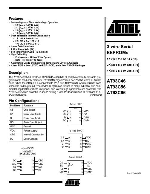
1Features•Low-voltage and Standard-voltage Operation–5.0 (V CC = 4.5V to 5.5V)–2.7 (V CC = 2.7V to 5.5V)–2.5 (V CC = 2.5V to 5.5V)–1.8 (V CC= 1.8V to 5.5V)•User-selectable Internal Organization –1K: 128 x 8 or 64 x 16–2K: 256 x 8 or 128 x 16–4K: 512 x 8 or 256 x 16•3-wire Serial Interface • 2 MHz Clock Rate (5V)•Self-timed Write Cycle (10 ms max)•High Reliability–Endurance: 1 Million Write Cycles –Data Retention: 100 Years•Automotive Grade and Extended Temperature Devices Available•8-lead PDIP , 8-lead JEDEC and EIAJ SOIC, and 8-lead TSSOP PackagesDescriptionThe AT93C46/56/66 provides 1024/2048/4096 bits of serial electrically erasable pro-grammable read only memory (EEPROM) organized as 64/128/256 words of 16 bits each, when the ORG pin is connected to VCC and 128/256/512 words of 8 bits each when it is tied to ground. The device is optimized for use in many industrial and com-mercial applications where low power and low voltage operations are essential. The AT93C46/56/66 is available in space-saving 8-lead PDIP and 8-lead JEDEC and EIAJSOIC packages.Pin ConfigurationsPin Name Function CS Chip Select SK Serial Data Clock DI Serial Data Input DO Serial Data Output GND Ground VCC Power Supply ORG Internal Organization DCDon ’t Connect8-lead PDIP8-lead SOIC Rotated (R)(1K JEDEC Only)8-lead SOIC (continued)8-lead TSSOP2AT93C46/56/660172O –08/01The AT93C46/56/66 is enabled through the Chip Select pin (CS), and accessed via a 3-wire serial interface consisting of Data Input (DI), Data Output (DO), and Shift Clock (SK). Upon receiving a READ instruction at DI, the address is decoded and the data is clocked out serially on the data output pin DO. The WRITE cycle is completely self-timed and no separate ERASE cycle is required before WRITE. The WRITE cycle is only enabled when the part is in the ERASE/WRITE ENABLE state. When CS is brought “high ” following the initiation of a WRITE cycle, the DO pin outputs the READY/BUSY status of the part.The AT93C46 is available in 4.5V to 5.5V, 2.7V to 5.5V, 2.5V to 5.5V, and 1.8V to 5.5V versions. The AT93C56/66 is available in 4.5V to 5.5V, 2.7V to 5.5V, and 2.5V to 5.5V versions.Block DiagramAbsolute Maximum Ratings*Operating Temperature..................................-55°C to +125°C *NOTICE:Stresses beyond those listed under “Absolute Maximum Ratings ” may cause permanent dam-age to the device. This is a stress rating only and functional operation of the device at these or any other conditions beyond those indicated in the operational sections of this specification is not implied. Exposure to absolute maximum rating conditions for extended periods may affect device reliabilityStorage Temperature.....................................-65°C to +150°C Voltage on Any Pinwith Respect to Ground.....................................-1.0V to +7.0V Maximum Operating Voltage..........................................6.25V DC Output Current........................................................5.0 mANotes:1. When the ORG pin is connected to VCC, the x 16 organization is selected. When it is connected to ground, the x 8 orga-nization is selected. If the ORG pin is left unconnected and the application does not load the input beyond the capability of the internal 1 Meg ohm pullup, then the x 16 organization is selected. The feature is not available on the 1.8V devices.2.For the AT93C46, if x 16 organization is the mode of choice and Pin 6 (ORG) is left unconnected, Atmel recommendsusing the AT93C46A device. For more details, see the AT93C46A datasheet.3AT93C46/56/660172O –08/01Note:1.This parameter is characterized and is not 100% tested.Note:1.V IL min and V IH max are reference only and are not tested.Pin Capacitance (1)Applicable over recommended operating range from T A = 25°C, f = 1.0 MHz, V CC = +5.0V (unless otherwise noted).Symbol Test Conditions Max Units Conditions C OUT Output Capacitance (DO)5pF V OUT = 0V C IN Input Capacitance (CS, SK, DI)5pFV IN = 0VDC CharacteristicsApplicable over recommended operating range from: T AI = -40°C to +85°C, V CC = +1.8V to +5.5V, T AC = 0°C to +70°C, V CC = +1.8V to +5.5V (unless otherwise noted).Symbol Parameter Test ConditionMin TypMax Unit V CC1Supply Voltage 1.8 5.5V V CC2Supply Voltage 2.5 5.5V V CC3Supply Voltage 2.7 5.5V V CC4Supply Voltage 4.55.5V I CC Supply Current V CC = 5.0V READ at 1.0 MHz 0.5 2.0mA WRITE at 1.0 MHz 0.5 2.0mA I SB1Standby Current V CC = 1.8V CS = 0V 00.1µA I SB2Standby Current V CC = 2.5V CS = 0V6.010.0µA I SB3Standby Current V CC = 2.7V CS = 0V 6.010.0µA I SB4Standby Current V CC = 5.0VCS = 0V1730µA I IL Input Leakage V IN = 0V to V CC 0.1 1.0µA I OL Output Leakage V IN = 0V to V CC 0.1 1.0µA V IL1(1)V IH1(1)Input Low Voltage Input High Voltage 4.5V ≤ V CC ≤ 5.5V -0.62.00.8V CC + 1V V IL2(1)V IH2(1)Input Low Voltage Input High Voltage 1.8V ≤ V CC ≤ 2.7V -0.6V CC x 0.7V CC x 0.3V CC + 1V V OL1V OH1Output Low Voltage Output High Voltage 4.5V ≤ V CC ≤ 5.5VI OL = 2.1 mA 0.4V I OH = -0.4 mA 2.4V V OL2V OH2Output Low Voltage Output High Voltage1.8V ≤ V CC ≤2.7VI OL = 0.15 mA 0.2V I OH = -100 µAV CC - 0.2V4AT93C46/56/660172O –08/01Note: 1.This parameter is characterized and is not 100% tested.AC CharacteristicsApplicable over recommended operating range from T A = -40°C to + 85°C, V CC = As Specified, CL = 1 TTL Gate and 100 pF (unless otherwise noted).SymbolParameter Test Condition Min TypMax Unitsf SKSK Clock Frequency4.5V ≤ V CC ≤5.5V 2.7V ≤ V CC ≤ 5.5V 2.5V ≤ V CC ≤ 5.5V 1.8V ≤ V CC ≤ 5.5V 0000210.50.25MHzt SKHSK High Time 4.5V ≤ V CC ≤ 5.5V 2.7V ≤ V CC ≤ 5.5V 2.5V ≤ V CC ≤ 5.5V 1.8V ≤ V CC ≤ 5.5V 2502505001000nst SKLSK Low Time 4.5V ≤ V CC ≤ 5.5V 2.7V ≤ V CC ≤ 5.5V 2.5V ≤ V CC ≤ 5.5V 1.8V ≤ V CC ≤ 5.5V 2502505001000nst CSMinimum CS Low Time4.5V ≤ V CC ≤5.5V 2.7V ≤ V CC ≤ 5.5V 2.5V ≤ V CC ≤ 5.5V 1.8V ≤ V CC ≤ 5.5V2502505001000nst CSSCS Setup Time Relative to SK 4.5V ≤ V CC ≤ 5.5V 2.7V ≤ V CC ≤ 5.5V 2.5V ≤ V CC ≤ 5.5V 1.8V ≤ V CC ≤ 5.5V 5050100200nst DISDI Setup Time Relative to SK 4.5V ≤ V CC ≤ 5.5V 2.7V ≤ V CC ≤ 5.5V 2.5V ≤ V CC ≤ 5.5V 1.8V ≤ V CC ≤ 5.5V100100200400nst CSHCS Hold Time Relative to SK 0nst DIHDI Hold Time Relative to SK 4.5V ≤ V CC ≤ 5.5V 2.7V ≤ V CC ≤ 5.5V 2.5V ≤ V CC ≤ 5.5V 1.8V ≤ V CC ≤ 5.5V 100100200400nst PD1Output Delay to ‘1’AC Test 4.5V ≤ V CC ≤ 5.5V 2.7V ≤ V CC ≤ 5.5V 2.5V ≤ V CC ≤ 5.5V 1.8V ≤ V CC ≤ 5.5V 2502505001000nst PD0Output Delay to ‘0’AC Test 4.5V ≤ V CC ≤ 5.5V 2.7V ≤ V CC ≤ 5.5V 2.5V ≤ V CC ≤ 5.5V 1.8V ≤ V CC ≤ 5.5V 2502505001000nst SVCS to Status Valid AC Test 4.5V ≤ V CC ≤ 5.5V 2.7V ≤ V CC ≤ 5.5V 2.5V ≤ V CC ≤ 5.5V 1.8V ≤ V CC ≤ 5.5V 2502505001000nst DFCS to DO in High ImpedanceAC Test CS = V IL4.5V ≤ V CC ≤5.5V 2.7V ≤ V CC ≤ 5.5V 2.5V ≤ V CC ≤ 5.5V 1.8V ≤ V CC ≤ 5.5V100100200400nst WPWrite Cycle Time 10ms 4.5V ≤ V CC ≤ 5.5V3ms Endurance (1)5.0V, 25°C, Page Mode1MWrite Cycles5AT93C46/56/660172O –08/01Instruction Set for the AT93C46Instruction SB Op Code Address DataCommentsx 8x 16x 8x 16READ 110A 6 - A 0A 5 - A 0Reads data stored in memory, at specified address.EWEN 10011XXXXX 11XXXX Write enable must precede all programming modes.ERASE 111A 6 - A 0A 5 - A 0Erase memory location A n - A 0.WRITE 101A 6 - A 0A 5 - A 0D 7 - D 0D 15 - D 0Writes memory location A n - A 0.ERAL 10010XXXXX 10XXXX Erases all memory locations. Valid only at V CC = 4.5V to 5.5V.WRAL 10001XXXXX 01XXXX D 7 - D 0D 15 - D 0Writes all memory locations. Valid only at V CC = 4.5V to 5.5V.EWDS10000XXXXX00XXXXDisables all programming instructions.6AT93C46/56/660172O –08/01Functional DescriptionThe AT93C46/56/66 is accessed via a simple and versatile 3-wire serial communication interface. Device operation is controlled by seven instructions issued by the host pro-cessor. A valid instruction starts with a rising edge of CS and consists of a Start Bit (logic “1”) followed by the appropriate Op Code and the desired memory Address location.READ (READ): The Read (READ) instruction contains the Address code for the mem-ory location to be read. After the instruction and address are decoded, data from the selected memory location is available at the serial output pin DO. Output data changes are synchronized with the rising edges of serial clock SK. It should be noted that a dummy bit (logic “0”) precedes the 8- or 16-bit data output string.ERASE/WRITE (EWEN): To assure data integrity, the part automatically goes into the Erase/Write Disable (EWDS) state when power is first applied. An Erase/Write Enable (EWEN) instruction must be executed first before any programming instructions can be carried out. Please note that once in the Erase/Write Enable state, programming remains enabled until an Erase/Write Disable (EWDS) instruction is executed or V CC power is removed from the part.ERASE (ERASE): The Erase (ERASE) instruction programs all bits in the specified memory location to the logical “1” state. The self-timed erase cycle starts once the ERASE instruction and address are decoded. The DO pin outputs the READY/BUSY status of the part if CS is brought high after being kept low for a minimum of 250 ns (t CS ).A logic “1” at pin DO indicates that the selected memory location has been erased, and the part is ready for another instruction.WRITE (WRITE): The Write (WRITE) instruction contains the 8 or 16 bits of data to be written into the specified memory location. The self-timed programming cycle, t WP , starts after the last bit of data is received at serial data input pin DI. The DO pin outputs the READY/BUSY status of the part if CS is brought high after being kept low for a minimum of 250 ns (t CS ). A logic “0” at DO indicates that programming is still in progress. A logic “1” indicates that the memory location at the specified address has been written with the data pattern contained in the instruction and the part is ready for further instructions. A READY/BUSY status cannot be obtained if the CS is brought high after the end of the self-timed programming cycle, t WP .ERASE ALL (ERAL): The Erase All (ERAL) instruction programs every bit in the mem-ory array to the logic “1” state and is primarily used for testing purposes. The DO pin outputs the READY/BUSY status of the part if CS is brought high after being kept low for a minimum of 250 ns (t CS ). The ERAL instruction is valid only at V CC = 5.0V ± 10%. WRITE ALL (WRAL): The Write All (WRAL) instruction programs all memory locations with the data patterns specified in the instruction. The DO pin outputs the READY/BUSY status of the part if CS is brought high after being kept low for a minimum of 250 ns (t CS ).The WRAL instruction is valid only at V CC = 5.0V ± 10%.ERASE/WRITE DISABLE (EWDS): To protect against accidental data disturb, the Erase/Write Disable (EWDS) instruction disables all programming modes and should be executed after all programming operations. The operation of the READ instruction is independent of both the EWEN and EWDS instructions and can be executed at any time.7AT93C46/56/660172O –08/01Timing DiagramsSynchronous Data TimingNote: 1.This is the minimum SK period.Notes:1.A 8 is a DON ’T CARE value, but the extra clock is required.2.A 7 is a DON ’T CARE value, but the extra clock is required.READ TimingOrganization Key for Timing DiagramsI/O AT93C46 (1K)AT93C56 (2K)AT93C66 (4K)x 8x 16x 8x 16x 8x 16A N A 6A 5A 8(1)A 7(2)A 8A 7D ND 7D 15D 7D 15D 7D 158AT93C46/56/660172O –08/01EWEN TimingEWDS TimingWRITE TimingWRAL Timing (1)Note:1.Valid only at V CC = 4.5V to 5.5V.9AT93C46/56/660172O –08/01ERASE TimingERAL Timing (1)Note:1.Valid only at V CC = 4.5V to 5.5V.10AT93C46/56/660172O –08/01AT93C46 Ordering Informationt WP (max)(ms)I CC (max)(µA)I SB (max)(µA)f MAX (kHz)Ordering Code Package Operation Range 10200030.02000AT93C46-10PC AT93C46-10SC AT93C46R-10SC AT93C46W-10SC AT93C46-10TC 8P38S18S18S28T Commercial (0°C to 70°C)30.02000AT93C46-10PI AT93C46-10SI AT93C46R-10SI AT93C46W-10SI AT93C46-10TI 8P38S18S18S28T Industrial (-40°C to 85°C)1080010.01000AT93C46-10PC-2.7AT93C46-10SC-2.7AT93C46R-10SC-2.7AT93C46W-10SC-2.7AT93C46-10TC-2.78P38S18S18S28T Commercial (0°C to 70°C)10.01000AT93C46-10PI-2.7AT93C46-10SI-2.7AT93C46R-10SI-2.7AT93C46W-10SI-2.7AT93C46-10TI-2.78P38S18S18S28TIndustrial (-40°C to 85°C)Package Type8P38-lead, 0.300" Wide, Plastic Dual Inline Package (PDIP)8S18-lead, 0.150" Wide, Plastic Gull Wing Small Outline (JEDEC SOIC)8S28-lead, 0.200" Wide, Plastic Gull Wing Small Outline (EIAJ SOIC)8T8-lead, 0.170" Wide, Thin Shrink Small Outline Package (TSSOP)OptionsBlank Standard Operation (4.5V to 5.5V)-2.7Low Voltage (2.7V to 5.5V)-2.5Low Voltage (2.5V to 5.5V)RRotated Pinout11AT93C46/56/660172O –08/011060010.0500AT93C46-10PC-2.5AT93C46-10SC-2.5AT93C46R-10SC-2.5AT93C46W-10SC-2.5AT93C46-10TC-2.58P38S18S18S28T Commercial (0°C to 70°C)10.0500AT93C46-10PI-2.5AT93C46-10SI-2.5AT93C46R-10SI-2.5AT93C46W-10SI-2.5AT93C46-10TI-2.58P38S18S18S28T Industrial (-40°C to 85°C)10800.1250AT93C46-10PC-1.8AT93C46-10SC-1.8AT93C46R-10SC-1.8AT93C46W-10SC-1.8AT93C46-10TC-1.88P38S18S18S28T Commercial (0°C to 70°C)0.1250AT93C46-10PI-1.8AT93C46-10SI-1.8AT93C46R-10SI-1.8AT93C46W-10SI-1.8AT93C46-10TI-1.88P38S18S18S28TIndustrial (-40°C to 85°C)AT93C46 Ordering Information (Continued)t WP (max)(ms)I CC (max)(µA)I SB (max)(µA)f MAX (kHz)Ordering Code Package Operation Range Package Type8P38-lead, 0.300" Wide, Plastic Dual Inline Package (PDIP)8S18-lead, 0.150" Wide, Plastic Gull Wing Small Outline (JEDEC SOIC)8S28-lead, 0.200" Wide, Plastic Gull Wing Small Outline (EIAJ SOIC)8T8-lead, 0.170" Wide, Thin Shrink Small Outline Package (TSSOP)OptionsBlank Standard Operation (4.5V to 5.5V)-2.7Low Voltage (2.7V to 5.5V)-2.5Low Voltage (2.5V to 5.5V)-1.8Low Voltage (1.8V to 5.5V)RRotated Pinout12AT93C46/56/660172O –08/01AT93C56 Ordering Informationt WP (max)(ms)I CC (max)(µA)I SB (max)(µA)f MAX (kHz)Ordering Code Package Operation Range 10200030.02000AT93C56-10PC AT93C56-10SC AT93C56W-10SC 8P38S18S2Commercial (0°C to 70°C)30.02000AT93C56-10PI AT93C56-10SI AT93C56W-10SI 8P38S18S2Industrial (-40°C to 85°C)1080010.01000AT93C56-10PC-2.7AT93C56-10SC-2.7AT93C56W-10SC-2.78P38S18S2Commercial (0°C to 70°C)10.01000AT93C56-10PI-2.7AT93C56-10SI-2.7AT93C56W-10SI-2.78P38S18S2Industrial (-40°C to 85°C)1060010.0500AT93C56-10PC-2.5AT93C56-10SC-2.5AT93C56W-10SC-2.58P38S18S2Commercial (0°C to 70°C)10.0500AT93C56-10PI-2.5AT93C56-10SI-2.5AT93C56W-10SI-2.58P38S18S2Industrial (-40°C to 85°C)Package Type8P38-lead, 0.300" Wide, Plastic Dual Inline Package (PDIP)8S18-lead, 0.150" Wide, Plastic Gull Wing Small Outline (JEDEC SOIC)8S28-lead, 0.200" Wide, Plastic Gull Wing Small Outline (EIAJ SOIC)OptionsBlank Standard Operation (4.5V to 5.5V)-2.7Low Voltage (2.7V to 5.5V)-2.5Low Voltage (2.5V to 5.5V)13AT93C46/56/660172O –08/01AT93C66 Ordering Informationt WP (max)(ms)I CC (max)(µA)I SB (max)(µA)f MAX (kHz)Ordering Code Package Operation Range 10200030.02000AT93C66-10PC AT93C66-10SC AT93C66W-10SC AT93C66-10TC 8P38S18S28T Commercial (0°C to 70°C)30.02000AT93C66-10PI AT93C66-10SI AT93C66W-10SI AT93C66-10TI 8P38S18S28T Industrial (-40°C to 85°C)1080010.01000AT93C66-10PC-2.7AT93C66-10SC-2.7AT93C66W-10SC-2.7AT93C66-10TC-2.78P38S18S28T Commercial (0°C to 70°C)10.01000AT93C66-10PI-2.7AT93C66-10SI-2.7AT93C66W-10SI-2.7AT93C66-10TI-2.78P38S18S28T Industrial (-40°C to 85°C)1060010.0500AT93C66-10PC-2.5AT93C66-10SC-2.5AT93C66W-10SC-2.5AT93C66-10TC-2.58P38S18S28T Commercial (0°C to 70°C)10.0500AT93C66-10PI-2.5AT93C66-10SI-2.5AT93C66W-10SI-2.5AT93C66-10TI-2.58P38S18S28T Industrial (-40°C to 85°C)10800.1250AT93C66-10PC-1.8AT93C66-10SC-1.8AT93C66W-10SC-1.8AT93C66-10TC-1.88P38S18S28T Commercial (0°C to 70°C)0.1250AT93C66-10PI-1.8AT93C66-10SI-1.8AT93C66W-10SI-1.8AT93C66-10TI-1.88P38S18S28TIndustrial (-40°C to 85°C)Package Type8P38-lead, 0.300" Wide, Plastic Dual Inline Package (PDIP)8S18-lead, 0.150" Wide, Plastic Gull Wing Small Outline (JEDEC SOIC)8S28-lead, 0.200" Wide, Plastic Gull Wing Small Outline (EIAJ SOIC)8T8-lead, 0.170" Wide, Thin Shrink Small Outline Package (TSSOP)OptionsBlank Standard Operation (4.5V to 5.5V)-2.7Low Voltage (2.7V to 5.5V)-2.5Low Voltage (2.5V to 5.5V)-1.8Low Voltage (1.8V to 5.5V)Packaging Information14AT93C46/56/660172O–08/01© Atmel Corporation 2001.Atmel Corporation makes no warranty for the use of its products, other than those expressly contained in the Company ’s standard warranty which is detailed in Atmel ’s Terms and Conditions located on the Company ’s web site. The Company assumes no responsibility for any errors which may appear in this document, reserves the right to change devices or specifications detailed herein at any time without notice, and does not make any commitment to update the information contained herein. No licenses to patents or other intellectual property of Atmel are granted by the Company in connection with the sale of Atmel products, expressly or by implication. Atmel ’s products are not authorized for use as critical components in life support devices or systems.Atmel HeadquartersAtmel Product OperationsCorporate Headquarters2325 Orchard Parkway San Jose, CA 95131TEL (408) 441-0311FAX (408) 487-2600EuropeAtmel SarLRoute des Arsenaux 41Casa Postale 80CH-1705 Fribourg SwitzerlandTEL (41) 26-426-5555FAX (41) 26-426-5500AsiaAtmel Asia, Ltd.Room 1219Chinachem Golden Plaza 77 Mody Road Tsimhatsui East Kowloon Hong KongTEL (852) 2721-9778FAX (852) 2722-1369JapanAtmel Japan K.K.9F, Tonetsu Shinkawa Bldg.1-24-8 ShinkawaChuo-ku, Tokyo 104-0033JapanTEL (81) 3-3523-3551FAX (81) 3-3523-7581Atmel Colorado Springs1150 E. Cheyenne Mtn. Blvd.Colorado Springs, CO 80906TEL (719) 576-3300FAX (719) 540-1759Atmel GrenobleAvenue de Rochepleine BP 12338521 Saint-Egreve Cedex, France TEL (33) 4-7658-3000FAX (33) 4-7658-3480Atmel HeilbronnTheresienstrasse 2POB 3535D-74025 Heilbronn, Germany TEL (49) 71 31 67 25 94FAX (49) 71 31 67 24 23Atmel NantesLa Chantrerie BP 7060244306 Nantes Cedex 3, France TEL (33) 0 2 40 18 18 18FAX (33) 0 2 40 18 19 60Atmel RoussetZone Industrielle13106 Rousset Cedex, France TEL (33) 4-4253-6000FAX (33) 4-4253-6001Atmel Smart Card ICsScottish Enterprise Technology Park East Kilbride, Scotland G75 0QR TEL (44) 1355-357-000FAX (44) 1355-242-743e-mailliterature@Web Site BBS1-(408) 436-43090172O –08/01/xMATMEL ® is the registered trademark of Atmel.Other terms and product names may be the trademarks of others.。