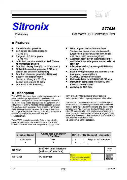
STSitronixST7036PreliminaryDot Matrix LCD Controller/DriverFeaturesz 5 x 8 dot matrix possiblez Low power operation support: -- 2.7 to 5.5Vz Range of LCD driver power -- 2.7 to 7.0Vz 4-bit, 8-bit, serial or 400kbits/s fast I 2C-bus MPU interface enabledz 80 x 8-bit display RAM (80 characters max.) z 10,240-bit character generator ROM for a total of 256 character fonts(max)z 64 x 8-bit character generator RAM(max) zSupport two display mode: 16-com x 100-seg and 80 ICON 24-com x 80-seg and 80 ICON z 16 x 5 –bit ICON RAM(max)zWide range of instruction functions:Display clear, cursor home, display on/off, cursor on/off, display character blink, cursor shift, display shift, double height fontzAutomatic reset circuit that initializes the controller/driver after power on and external reset pinz Internal oscillator(Frequency=540kHz) and external clockz Built-in voltage booster and follower circuit (low power consumption ) z COM/SEG direction selectablez Multi-selectable for CGRAM/CGROM size z Instruction compatible to ST7066U and KS0066U and HD44780 zAvailable in COG typeDescriptionT he ST7036 dot-matrix liquid crystal display controller anddriver LSI displays alphanumeric, Japanese kanacharacters, and symbols. It can be configured to drive a dot-matrix liquid crystal display under the control of a 4-/8-bit, serial or fast I 2C interface microprocessor. Since all the functions such as display RAM, character generator, and liquid crystal driver, required for driving a dot-matrix liquid crystal display are internally provided on one chip, a minimal system can be interfaced with this controller/driver.The ST7036 character generator ROM is extended to generate 256 5x8dot character fonts for a total of 256 different character fonts. The low power supply (2.7V to5.5V) of the ST7036 is suitable for any portablebattery-driven product requiring low power dissipation.The ST7036 LCD driver consists of 17 common signal drivers and 100 segment signal drivers. And the second mode is consists of 25 common signal and 80 segment signal drivers. The maximum display RAM size can be either 80 characters in 1-line display or 40 characters in 2-line display or 16 characters in 3-line. A single ST7036 can display up to one 20-character line or two 20-character lines or three 16-character lines. No extra drivers can be cascaded.product NameCharacter generatorROM SizeOPR1OPR2Support CharacterST7036-0A 256 1 1 English / Japan/Europe- - - - -Table 4 Correspondence between Character Codes and Character PatternsCGRAM/CGROM arrangement with (OPR1, OPR2)=When BS=”High”, the bias will be 1/4When BS=”Low”, the bias will be 1/5Set ICON RAM address to AC.This instruction makes ICON data available from MPU. When IS=1 at Extension mode,Reset FunctionInitializing by Internal Reset CircuitAn internal reset circuit automatically initializes the ST7036 when the power is turned on. Thefollowing instructions are executed during the initialization. The busy flag (BF) is kept in the busy state (BF = 1) until the initialization ends. The busy state lasts for 40 ms after VDD rises to stable.1. Displayclearset:2. FunctionDL = 1; 8-bit interface dataN = 0; 1-line displayDH=0; normal 5x8 fontIS[2:1]=(0,0); use instruction table 03. Display on/off control:D = 0; Display offC = 0; Cursor offB = 0; Blinking off4. Entry mode set:I/D = 1; Increment by 1S = 0; No shift5. 3 line: FX=11/2 line: FX=0control6. ICONIon=0; ICON off7. PowercontrolBS=0; 1/5biasBon=0; booster offFon=0; follower off(C5,C4,C3,C2,C1,C0)=(1,0,0,0,0,0)(Rab2,Rab1,Rab0)=(0,1,0)8. Double Height Position SelectUD=0, double height font is show on Com9~Com24.Note:If the electrical characteristics conditions listed under the table Power Supply Conditions UsingInternal Reset Circuit are not met, the internal reset circuit will not operate normally and will failto initialize the ST7036.When internal Reset Circuit not operate,ST7036 can be reset by XRESET pin from MPU control signal.¾Initial Program Code Example For 8051 MPU(8 Bit Interface): ;--------------------------------------------------------------------------------- INITIAL_START:CALL DELAY40mSMOV A,#38H ;FUNCTION SETCALL WRINS_NOCHK ;8 bit, N=1,5*7dotCALL DELAY30uSMOV A,#38H ;FUNCTION SETCALL WRINS_NOCHK ;8 bit, N=1,5*7dotCALL DELAY30uSMOV A,#14H ;set biasCALL WRINS_CHKCALL DELAY30uSMOV A,#78H ;Contrast set adjustmentCALL WRINS_CHKCALL DELAY30uSMOV A,#5EH ;Power/ICON/Contrast controlCALL WRINS_CHKCALL DELAY30uSMOV A,#6AH ;Follower controlCALL WRINS_CHKCALL DELAY30uSMOV A,#0CH ;DISPLAY ONCALL WRINS_CHKCALL DELAY30uSMOV A,#01H ;CLEAR DISPLAYCALL WRINS_CHKCALL DELAY2mSMOV A,#06H ;ENTRY MODE SETCALL WRINS_CHK ;CURSOR MOVES TO RIGHTCALL DELAY30uS;---------------------------------------------------------------------------------MAIN_START:XXXXXXXXXXXXXXXX;--------------------------------------------------------------------------------- WRINS_CHK:CALL CHK_BUSYWRINS_NOCHK:CLR RS ;EX: Port 3.0CLR RW ;EX: Port 3.1SETB E ;EX:Port 3.2MOV P1,A ;EX:Port 1=Data BusCLR EMOV P1,#FFH ;For Check Busy FlagRET;---------------------------------------------------------------------------------FlagBusy;CheckCHK_BUSY:CLR RSSETB RWSETB EJB P1.7,$CLR ERET元器件交易网ST70364-bit Interface (fosc=380kHz)V1.141/722003/12/24元器件交易网ST7036Initial Program Code Example For 8051 MPU(4 Bit Interface):;------------------------------------------------------------------INITIAL_START: CALL DELAY40mS MOV A,#30H ; FUNCTION SET CALL WRINS_ONCE ; 8 bit, DL = 1 CALL DELAY2mS MOV CALL CALL MOV CALL CALL CALL MOV CALL CALL MOV CALL CALL MOV CALL CALL MOV CALL CALL MOV CALL CALL MOV CALL CALL MOV CALL CALL MOV CALL CALL A,#30H ; FUNCTION SET WRINS_ONCE ; 8 bit, DL = 1 DELAY30uS A,#30H ; FUNCTION SET WRINS_ONCE ; 8 bit, DL = 1 DELAY30uS CHK_BUSY A,#20H ; FUNCTION SET WRINS_ONCE ; 4 bit, DL = 0 DELAY30uS A,#29H WRINS_CHK DELAY30uS A,#14H WRINS_CHK DELAY30uS A,#78H WRINS_CHK DELAY30uS A,#5EH WRINS_CHK DELAY30uS A,#6AH WRINS_CHK DELAY30uS A,#0CH WRINS_CHK DELAY30uS A,#01H WRINS_CHK DELAY2mS ; FUNCTION SET ; 4 bit, DL = 0, N = 1, ; IS2 = 0, IS1 = 1 ;bias;Contrast set;Power/ICON/Contrast;Follower control;DISPLAY ONXXXX ;------------------------------------------------------------------WRINS_CHK: CALL CHK_BUSY WRINS_NOCHK: PUSH A ANL A,#F0H CLR RS ;EX: Port 3.0 CLR RW ;EX: Port 3.1 SETB E ;EX: Port 3.2 MOV P1,A ;EX:Port1=Data Bus CLR E POP A SWAP A WRINS_ONCE: ANL A,#F0H CLR RS CLR RW SETB E MOV P1,A CLR E MOV P1,#FFH ;For Check Bus Flag RET ;------------------------------------------------------------------CHK_BUSY: ;Check Busy Flag PUSH A MOV P1,#FFH $1 CLR RS SETB RW SETB E MOV A,P1 CLR E MOV P1,#FFH CLR RS SETB RW SETB E NOP CLR E JB A.7,$1 POP A RET;CLEAR DISPLAYMOV A,#06H ;ENTRY MODE SET CALL WRINS_CHK CALL DELAY30uS ;------------------------------------------------------------------MAIN_START: XXXX XXXX XXXXV1.142/722003/12/24元器件交易网ST7036Serial interface & IIC interface ( fosc = 380kHz )POWER ON and external resetWait time >40mS After VDD stableFunction setRS 0 R/W DB7 DB6 DB5 DB4 DB3 DB2 DB1 DB0 0 0 0 1 1 N DH IS2 IS1Wait time >26.3μSFunction setRS 0 R/W DB7 DB6 DB5 DB4 DB3 DB2 DB1 DB0 0 0 0 1 1 N DH IS2 IS1Wait time >26.3μSInternal OSC frequencyRS 0 R/W DB7 DB6 DB5 DB4 DB3 DB2 DB1 DB0 0 0 0 0 1 BS F2 F1 F0 RS 0Power/ICON/Contrast controlR/W DB7 DB6 DB5 DB4 DB3 DB2 DB1 DB0 C5 C4 0 0 1 0 1 Ion BonWait time >26.3μSWait time >26.3μSContrast setRS 0 R/W DB7 DB6 DB5 DB4 DB3 DB2 DB1 DB0 0 0 1 1 1 C3 C2 C1 C0 RS 0Follower controlR/W DB7 DB6 DB5 DB4 DB3 DB2 DB1 DB0 0 0 1 1 0 Fon Rab2 Rab1 Rab0Wait time >26.3μSWait time >200mS (for power stable)Display ON/OFF controlRS 0 R/W DB7 DB6 DB5 DB4 DB3 DB2 DB1 DB0 0 0 0 0 0 1 D C BWait time >26.3μSInitialization endV1.143/722003/12/24元器件交易网ST7036Initial Program Code Example For 8051 MPU ( Serial Interface ) : ;--------------------------------------------------------------------------------INITIAL_START: CALL HARDWARE_RESET CALL DELAY40mS MOV A,#38H ;FUNCTION SET CALL WRINS_NOCHK ;8 bit, N=1,5*7dot CALL DELAY30uS MOV A,#39H ;FUNCTION SET CALL WRINS_NOCHK ;8 bit, N=1,5*7dot,IS=1 CALL DELAY30uS MOV A,#14H ;bias CALL WRINS_NOCHK CALL DELAY30uS MOV A,#78H ;Contrast set CALL WRINS_NOCHK CALL DELAY30uS MOV A,#5EH ;Power/ICON/Contrast control CALL WRINS_NOCHK CALL DELAY30uS MOV A,#6AH ;Follower control CALL WRINS_NOCHK CALL DELAY200mS ;for power stable MOV A,#0CH ;DISPLAY ON CALL WRINS_NOCHK CALL DELAY30uS MOV A,#01H ;CLEAR DISPLAY CALL WRINS_NOCHK CALL DELAY2mS MOV A,#06H ;ENTRY MODE SET CALL WRINS_NOCHK ;CURSOR MOVES TO RIGHT CALL DELAY30uS ;--------------------------------------------------------------------------------MAIN_START: XXXX XXXX XXXX XXXX . . .;--------------------------------------------------------------------------------WRINS_NOCHK: PUSH 1 MOV R1,#8 CLR RS $1 RLC A MOV SI,C SETB SCL NOP CLR SCL DJNZ R1,$1 POP 1 CALL RET DLY1.5mSV1.144/722003/12/24元器件交易网ST7036 Interfacing to the MPUThe ST7036 can send data in two 4-bit operations/one 8-bit operation, serial 1 bit operation or fast I2C operation, thus allowing interfacing with 4-bit, 8-bit or I2C MPU.For 4-bit interface data, only four bus lines (DB4 to DB7) are used for transfer. Bus lines DB0 to DB3are disabled. The data transfer between the ST7036 and the MPU is completed after the 4-bit data has been transferred twice. As for the order of data transfer, the four high order bits (for 8-bit operation, DB4 to DB7) are transferred before the four low order bits (for 8-bit operation, DB0 to DB3). The busy flag must be checked (one instruction) after the 4-bit data has been transferred twice. Two more 4-bit operations then transfer the busy flag and address counter data.Example of busy flag check timing sequenceCSBRSR/WEInternal operationFunctioningDB7IR7IR3AC3Not BusyAC3IR7IR3Instruction writeBusy flag checkBusy flag checkInstruction writeIntel 8051 interface(4 Bit)P1.0 to P1.3 P3.0 P3.1 P3.2 P3.3 Intel 8051 Serial4COM1 to COM16/24 DB4 to DB7 RS R/W E CSB ST703616/24SEG1 to SEG100/80100/80V1.145/722003/12/24元器件交易网ST7036For 8-bit interface data, all eight bus lines (DB0 to DB7) are used.Example of busy flag check timing sequenceCSBRSR/WEInternal operationFunctioningDB7DataBusyBusyNot BusyDataInstruction writeBusy flag checkBusy flag checkBusy flag checkInstruction writeIntel 8051 interface(8 Bit)P1.0 to P1.7 P3.0 P3.1 P3.2 P3.3 Intel 8051 Serial8COM1 to COM16/24 DB0 to DB7 RS R/W E CSB ST703616/24SEG1 to 100/80 SEG100/80V1.146/722003/12/24元器件交易网ST7036For serial interface data, only two bus lines (DB6 to DB7) are used.Example of timing sequenceCSBSID7D6D5D4D3D2D1D0D7D6D5D4D3D2SCL1 2 3 4 5 6 7 8 9 10 11 12 13 14RSIntel 8051 interface ( Serial 4-line )P1.6 to P1.7 P3.0 P3.32COM1 to COM16/24 SI , SCL RS CSB16/24SEG1 to 100/80 SEG100/80 Intel 8051 Serial ST7036V1.147/722003/12/24元器件交易网ST7036For I2C interface data, all eight bus lines (DB0 to DB7) are used.Example of timing sequenceSDAD7D6D5D4D3D2D1D0ACK.......D0ACKSCL1 2 3 4 5 6 7 8 9......Intel 8051 interface ( I2C interface )V1.148/722003/12/24元器件交易网ST7036 Supply Voltage for LCD DriveWhen external bias resistors are used (OPF1=1,OPF2=1)VCC (2.7~ 5.5V) Vext VCC (2.7~ 5.5V) VextOPF1 OPF2 VDD VOUT VIN CAP1P CAP1NOPF1 OPF2VDD V0 V1 V2 V3 R V4 R VSS VR R R VLCDV0 V1 V2 V3 V4VR R R VLCD R RVOUT VIN CAP1P CAP1NVSS 1/4 bias GND 1/5 biasGNDWhen built-in bias resistors(9.6KΩ) are used (OPF1=1,OPF2=0)VCC(2.7~5.5V) VextOPF1 VOUT VIN CAP1P CAP1NVDD V0 V1 V2 V3 V4 VSS VLCD VROPF2GNDV1.149/722003/12/24元器件交易网ST7036When built-in bias resistors(3.3KΩ) are used (OPF1=0,OPF2=1)VCC (2.7~ 5.5V) VextOPF2 VOUT VIN CAP1P CAP1NVDD V0 V1 V2 V3 V4 VSS VLCD VROPF1GNDWhen built-in voltage followers with external Vout are used (OPF1=0,OPF2=0 and instruction setting Bon=0,Fon=1)Vext ≧ V0 VCC (2.7~ 5.5V) Don't need to connect stable capacitor when use internal follower circuitVOUT VIN CAP1P CAP1NVDD V0 V1 V2 V3 V4 VLCDOPF1 OPF2 VSSGNDV1.150/722003/12/24。