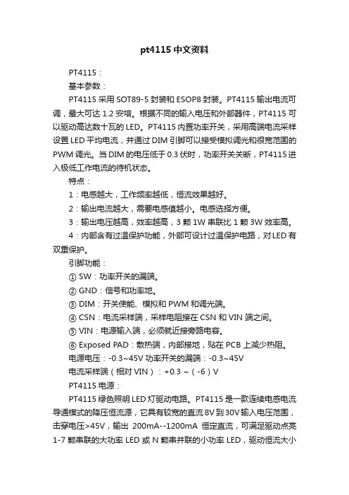
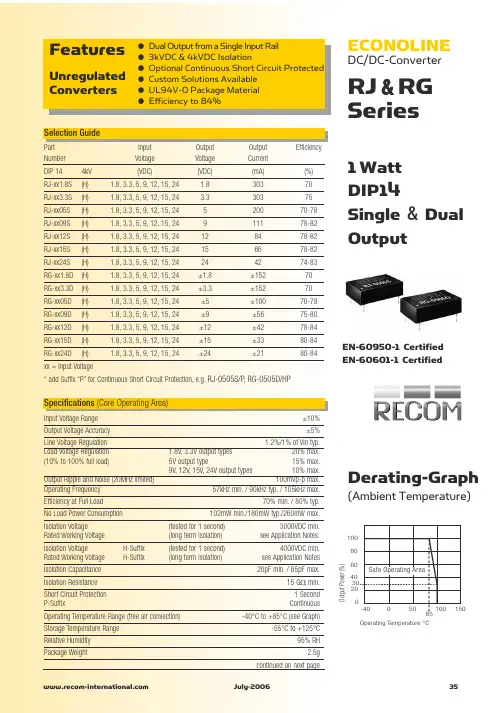
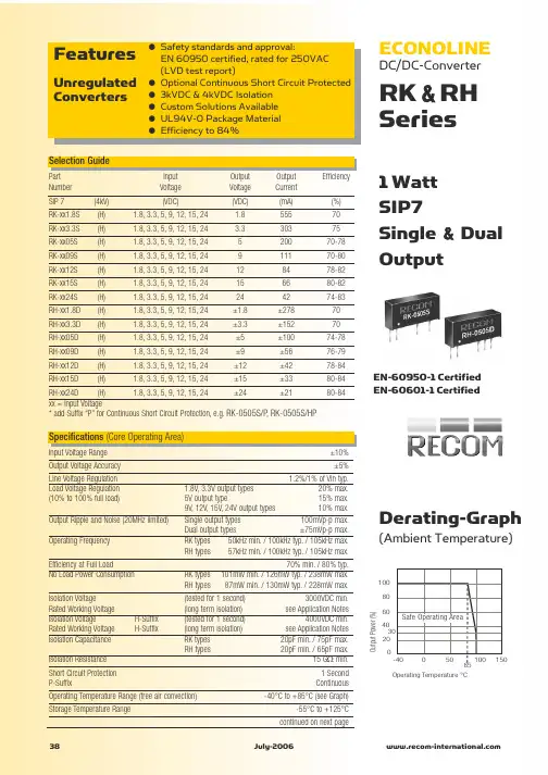
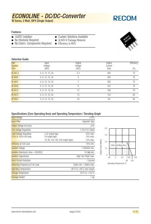
RT8009-15PJ5中文资料
- 格式:pdf
- 大小:281.94 KB
- 文档页数:13
RT80091DS8009-03 March 2007www.richtek.comFeatures+2.5V to +5.5V Input RangeAdjustable Output From 0.5V to VIN1.0V, 1.2V, 1.5V, 1.8V, 2.5V and 3.3V Fixed/Adjustable Output Voltage600mA Output Current95% EfficiencyNo Schottky Diode Required1.25MHz Fixed-Frequency PWM OperationSmall SOT-23-5 and TSOT-23-5 PackageRoHS Compliant and 100% Lead (Pb)-FreeApplicationsCellular TelephonesPersonal Information AppliancesWireless and DSL ModemsMP3 PlayersPortable Instruments1.25MHz, 600mA, High Efficiency PWM Step-Down DC/DCConverterGeneral DescriptionThe RT8009 is a high-efficiency pulse-width-modulated(PWM) step-down DC-DC converter. Capable of delivering600mA output current over a wide input voltage range from2.5 to 5.5V, the RT8009 is ideally suited for portableelectronic devices that are powered from 1-cell Li-ionbattery or from other power sources within the range suchas cellular phones, PDAs and handy-terminals.Internal synchronous rectifier with low RDS(ON) dramaticallyreduces conduction loss at PWM mode. No externalSchottky diode is required in practical application. TheRT8009 automatically turns off the synchronous rectifierwhile the inductor current is low and enters discontinuousPWM mode. This can increase efficiency at light loadcondition.The RT8009 enters Low-Dropout mode when normal PWMcannot provide regulated output voltage by continuouslyturning on the upper P-MOSFET. RT8009 enter shutdownmode and consumes less than 0.1uA when EN pin is pulledlow.The switching ripple is easily smoothed-out by smallpackage filtering elements due to a fixed operationfrequency of 1.25MHz. This along with small SOT-23-5and TSOT-23-5 package provides small PCB areaapplication. Other features include soft start, lower internalreference voltage with 2% accuracy, over temperatureprotection, and over current protection.Note :RichTek Pb-free and Green products are :`RoHS compliant and compatible with the current require- ments of IPC/JEDEC J-STD-020.`Suitable for use in SnPb or Pb-free soldering processes.`100% matte tin (Sn) plating.Ordering InformationPin Configurations(TOP VIEW)SOT-23-5/TSOT-23-5VINGNDENLX23541FB/VOUTRT8009(- )Package TypeB : SOT-23-5J5 : TSOT-23-5Operating Temperature RangeP : Pb Free with Commercial StandardG : Green (Halogen Free with Commer- cial Standard)Output VoltageDefault : Adjustable10 : 1.0V12 : 1.2V15 : 1.5V18 : 1.8V25 : 2.5V33 : 3.3V元器件交易网www.cecb2b.comRT80092DS8009-03 March 2007www.richtek.comTypical Application CircuitFigure 1. Fixed Voltage RegulatorFigure 2. Adjustable Voltage Regulator0.5VVand 1MR2R1 withR2R11 x VVREF(Typ.)REFOUT=Ω≤+⎟⎠⎞⎜⎝⎛+=Layout GuideLayout note:1.The distance that CIN connects to VIN is as close as possible (Under 2mm).2. COUT should be placed near RT8009.Figure 3VINGNDENLX23541VOUTVINCINVOUTLGNDCOUTVINGNDENLX23541FBVINCINVOUTLGNDVOUTCOUTR2R1C14.7uF10uFVINLXGNDRT8009ENVOUT4.7uH2.5V to 5.5VVINVOUTCINL45132COUT4.7uF10uFVINLXGNDRT8009ENFB4.7uH2.5V to 5.5VVINVOUTCINL45132COUTR1R2C1元器件交易网www.cecb2b.comRT80093DS8009-03 March 2007www.richtek.comFunction Block DiagramFunctional Pin DescriptionPin Number Pin Name Pin Function 1 VIN Power Input. 2 GND Ground. 3 EN Chip Enable (Active High, do not leave EN pin floating, and VEN < VIN + 0.6V). 4 FB/VOUT Feedback Input Pin. 5 LX Pin for Switching. COMPRCRS1RS2ENVINLXFB/VOUTUVLO &Power GoodDetectorVREFSlopeCompensationCurrentSenseOSC &ShutdownControlZeroDetectorCurrentLimitDetectorDriverControlLogicPWMComparatorErrorAmplifierGND元器件交易网www.cecb2b.comRT80094DS8009-03 March 2007www.richtek.comAbsolute Maximum Ratings (Note 1)Supply Input Voltage------------------------------------------------------------------------------------------------------6.5VEnable, FB Voltage-------------------------------------------------------------------------------------------------------VIN + 0.6VPower Dissipation, PD @ TA = 25°CSOT-23-5, TSOT-23-5-----------------------------------------------------------------------------------------------------0.4WPackage Thermal Resistance (Note 4)SOT-23-5, TSOT-23-5, θJA-----------------------------------------------------------------------------------------------250°C/WSOT-23-5, TSOT-23-5, θJC-----------------------------------------------------------------------------------------------130°C/WJunction Temperature Range--------------------------------------------------------------------------------------------150°CLead Temperature (Soldering, 10 sec.)-------------------------------------------------------------------------------260°CStorage Temperature Range--------------------------------------------------------------------------------------------−65°C to 150°CESD Susceptibility (Note 2)HBM (Human Body Mode)----------------------------------------------------------------------------------------------2kVMM (Machine Mode)------------------------------------------------------------------------------------------------------200VElectrical Characteristics(VIN = 3.6V, VOUT = 2.5V, VREF = 0.5V, L = 4.7μH, CIN = 4.7μF, COUT = 10μF, TA = 25°C, IMAX = 600mA unless otherwise specified)Parameter Symbol Test Conditions Min Typ Max Units Input Voltage Range VIN 2.5 -- 5.5 V Quiescent Current IQ IOUT = 0mA, VFB = VREF + 5% -- 50 100 μA Shutdown Current ISHDN EN = GND -- 0.1 1 μA Reference Voltage VREF For adjustable output voltage 0.49 0.5 0.51 V Adjustable Output Range VOUT VREF -- VIN − 0.2 V Output Voltage Accuracy Fix ΔVOUT VIN = 2.5 to 5.5V, VOUT = 1.0V 0A < IOUT < 600mA −3 -- +3 % ΔVOUT VIN = 2.5 to 5.5V, VOUT = 1.2V 0A < IOUT < 600mA −3 -- +3 % ΔVOUT VIN = 2.5 to 5.5V, VOUT = 1.5V 0A < IOUT < 600mA −3 -- +3 % ΔVOUT VIN = 2.5 to 5.5V, VOUT = 1.8V 0A < IOUT < 600mA −3 -- +3 % ΔVOUT VIN = VOUT + ΔV to 5.5V (Note 5) VOUT = 2.5V, 0A < IOUT < 600mA −3 -- +3 % ΔVOUT VIN = VOUT + ΔV to 5.5V (Note 5) VOUT = 3.3V, 0A < IOUT < 600mA −3 -- +3 % ΔVOUT VIN = VOUT + 0.2V to 5.5V 0A < IOUT < 600mA −3 -- +3 % To be continuedRecommended Operating Conditions (Note 3)Supply Input Voltage------------------------------------------------------------------------------------------------------2.5V to 5.5VJunction Temperature Range--------------------------------------------------------------------------------------------−40°C to 125°CAmbient Temperature Range--------------------------------------------------------------------------------------------−40°C to 85°C元器件交易网www.cecb2b.com