MC74HCT541ADWG中文资料
- 格式:pdf
- 大小:114.60 KB
- 文档页数:8
© Semiconductor Components Industries, LLC, 2006June, 2006 − Rev. 51Publication Order Number:
MC74HCT541A/DMC74HCT541A
Octal 3−State Non−Inverting
Buffer/Line Driver/
Line Receiver With
LSTTL−Compatible Inputs
High−Performance Silicon−Gate CMOS
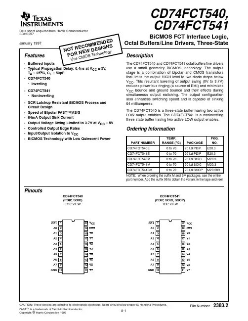
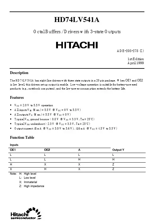
The MC74HCT541A is identical in pinout to the LS541. Thisdevice may be used as a level converter for interfacing TTL or NMOSoutputs to high speed CMOS inputs.The HCT541A is an octal non−inverting buffer/line driver/linereceiver designed to be used with 3−state memory address drivers,clock drivers, and other bus−oriented systems. This device featuresinputs and outputs on opposite sides of the package and two ANDedactive−low output enables.
Features•Output Drive Capability: 15 LSTTL Loads•TTL/NMOS−Compatible Input Levels•Outputs Directly Interface to CMOS, NMOS and TTL•Operating Voltage Range: 4.5 to 5.5 V•Low Input Current: 1mA•In Compliance With the JEDEC Standard No. 7A Requirements•Chip Complexity: 134 FETs or 33.5 Equivalent Gates•Pb−Free Packages are Available*18Y12A1
17Y23A2
16Y34A3
15Y45A4
14Y56A5
13Y67A6
12Y78A7
11Y89A8
OE1OE21
19OutputEnablesDataInputsNon−InvertingOutputs
PIN 20 = VCCPIN 10 = GNDLOGIC DIAGRAM
*For additional information on our Pb−Free strategy and soldering details, pleasedownload the ON Semiconductor Soldering and Mounting Techniques
Reference Manual, SOLDERRM/D.
20
1HCT541AAWLYYWWGhttp://onsemi.com
MARKING DIAGRAMS
20
1
1
1PDIP−20N SUFFIXCASE 738
SOIC−20WBDW SUFFIXCASE 751DMC74HCT541ANAWLYYWWG
A= Assembly LocationWL, L= Wafer LotYY, Y= YearWW, W= Work WeekG or G= Pb−Free Package(Note: Microdot may be in either location)
See detailed ordering and shipping information in the packagedimensions section on page 5 of this data sheet.ORDERING INFORMATIONTSSOP−20DT SUFFIXCASE 948E
SOEIAJ−20F SUFFIXCASE 96774HCT541AAWLYWWG
1120
1
20
1HCT541AALYWGG元器件交易网www.cecb2b.comMC74HCT541A
http://onsemi.com2PINOUT: 20−LEAD PACKAGES19201817161514
2134567VCC13
812
911
10OE2Y1Y2Y3Y4Y5Y6Y7Y8
OE1A1A2A3A4A5A6A7A8GND
LLHXLLXHLHXXFUNCTION TABLE
InputsOutput YOE1OE2ALHZZZ = High ImpedanceX = Don’t Care(Top View)MAXIMUM RATINGS
SymbolParameterValueUnitVCCDC Supply Voltage (Referenced to GND)– 0.5 to + 7.0V
VinDC Input Voltage (Referenced to GND)– 0.5 to VCC + 0.5V
VoutDC Output Voltage (Referenced to GND)– 0.5 to VCC + 0.5V
IinDC Input Current, per Pin±20mA
IoutDC Output Current, per Pin±35mA
ICCDC Supply Current, VCC and GND Pins±75mA
PDPower Dissipation in Still AirPlastic DIP†SOIC Package†750500mW
TstgStorage Temperature Range
– 65 to + 150_C
TLLead Temperature, 1 mm from Case for 10 SecondsPlastic DIP or SOIC Package260_C
Stresses exceeding Maximum Ratings may damage the device. Maximum Ratings are stressratings only. Functional operation above the Recommended Operating Conditions is not implied.Extended exposure to stresses above the Recommended Operating Conditions may affect devicereliability.†Derating—Plastic DIP: – 10 mW/_C from 65_ to 125_CSOIC Package: – 7 mW/_C from 65_ to 125_CFor high frequency or heavy load considerations, see Chapter 2 of the ON Semiconductor High−Speed CMOS Data Book (DL129/D).
RECOMMENDED OPERATING CONDITIONS
SymbolParameterMinMaxUnitVCCDC Supply Voltage (Referenced to GND)4.55.5V
Vin, VoutDC Input Voltage, Output Voltage(Referenced to GND)0VCCV
TAOperating Temperature Range, All Package Types– 55+ 125_C
tr, tfInput Rise/Fall Time (Figure 1)0500nsThis device contains protectioncircuitry to guard against damage dueto high static voltages or electricfields. However, precautions must betaken to avoid applications of anyvoltage higher than maximum ratedvoltages to this high−impedancecircuit. For proper operation, Vin andVout should be constrained to therange GND v (Vin or Vout) v VCC.Unused inputs must always be tiedto an appropriate logic voltage level(e.g., either GND or VCC). Unusedoutputs must be left open.元器件交易网www.cecb2b.comMC74HCT541A
http://onsemi.com3DC CHARACTERISTICS (Voltages Referenced to GND)
VCCVGuaranteed LimitSymbolParameterCondition−55 to 25°C≤85°C≤125°CUnitVIHMinimum High−Level Input VoltageVout = 0.1V or VCC − 0.1V|Iout| ≤ 20mA4.55.52.02.02.02.02.02.0V
VILMaximum Low−Level Input VoltageVout = 0.1V or VCC − 0.1V|Iout| ≤ 20mA4.55.50.80.80.80.80.80.8V
VOHMinimum High−Level Output VoltageVin = VIH or VIL|Iout| ≤ 20mA4.55.54.45.44.45.44.45.4V
Vin = VIH or VIL|Iout| ≤ 6.0mA4.53.983.843.70
VOLMaximum Low−Level Output VoltageVin = VIH or VIL|Iout| ≤ 20mA4.55.50.10.10.10.10.10.1V
Vin = VIH or VIL|Iout| ≤ 6.0mA4.50.260.330.40
IinMaximum Input Leakage CurrentVin = VCC or GND5.5±0.1±1.0±1.0mA
IOZMaximum 3−State Leakage CurrentOutput in High Impedance StateVin = VIL or VIHVout = VCC or GND5.5±0.5±5.0±10.0mA
ICCMaximum Quiescent Supply Current(per Package)Vin = VCC or GNDIout = 0mA5.5440160mA