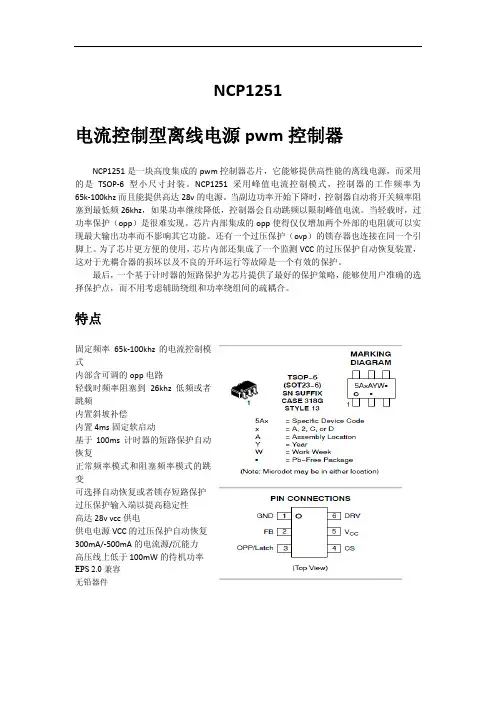
LFX125B-3F900C中文资料
- 格式:pdf
- 大小:972.62 KB
- 文档页数:89
www.latticesemi.com1
xpga_04ispXPGA Family
March 2003Preliminary Data SheetTM
© 2003 Lattice Semiconductor Corp. All Lattice trademarks, registered trademarks, patents, and disclaimers are as listed at www.latticesemi.com/legal. All other brandor product names are trademarks or registered trademarks of their respective holders. The specifications and information herein are subject to change without notice.■Non-volatile, Infinitely Reconfigurable •Instant-on - Powers up in microseconds via on-chip E2CMOS® based memory•No external configuration memory•Excellent design security, no bit stream to intercept•Reconfigure SRAM based logic in milliseconds
■High Logic Density for System-level Integration•139K to 1.25M system gates•160 to 496 I/O•1.8V, 2.5V, and 3.3V VCC operation•Up to 414Kb sysMEM™ embedded memory
■High Performance Programmable Function Unit (PFU)•Four LUT-4 per PFU supports wide and narrow functions•Dual flip-flops per LUT-4 for extensive pipelining•Dedicated logic for adders, multipliers, multiplex-ers, and counters
■Variable-Length Interconnect Routing Technology•Optimum speed, power, and flexibility for logic interconnections
■
Flexible Memory Resources
•Multiple sysMEM Embedded RAM Blocks–Single port, Dual port, and FIFO operation•64-bit distributed memory in each PFU–Single port, Double port, FIFO, and Shift Register operation
■
Eight sysCLOCK™ Phase Locked Loops (PLLs) for Clock Management
•True PLL technology•10MHz to 320MHz operation•Clock multiplication and division•Phase adjustment•Shift clocks in 250ps steps
■
sysIO™ for High System Performance
•High speed memory support through SSTL and HSTL•Advanced buses supported through PCI, GTL+, LVDS, BLVDS, and LVPECL•Standard logic supported through LVTTL, LVCMOS 3.3, 2.5, and 1.8•Programmable drive strength for series termination•Programmable bus maintenance
■
sysHSI™ Capability for Ultra Fast Serial Communications
•Up to 850Mbps performance•Up to 20 channels per device•Built in Clock Data Recovery (CDR) and Serialization and De-serialization (SERDES)
■
Flexible Programming, Reconfiguration, and Testing
•IEEE 1532 and 1149.1 compliant •Microprocessor configuration interface•Program E
2
CMOS while operating from SRAM
Table 1. ispXPGA Family Selection Guide ispXPGA 125ispXPGA 200ispXPGA 500ispXPGA 1200
System Gates139K210K476K1.25M
PFUs48467617643844
LUT-4s19362704705615376
Logic FFs3.8K5.4K14.1K30.7K
sysMEM Memory92K111K184K414K
Distributed Memory30K43K112K246K
EBR20244090
sysHSI Channels481220
User I/O160/176160/208336496
Packaging256 fpBGA516 fpBGA
1
256 fpBGA516 fpBGA
1
516 fpBGA
1
900 fpBGA680 fpSBGA
1
900 fpBGA
1.Thermally enhanced package.
Note: LFX1200B/C is preliminary, LFX125/200/500B/C information is advanced.www.cecb2b.com
Lattice SemiconductorispXPGA Family Data Sheet
2 ispXPGA Family Overview
The ispXPGA family of devices allows the creation of high-performance logic designs that are both non-volatile andinfinitely re-programmable. Other FPGA solutions force a compromise being either re-programmable or non-vola-tile. This family couples this capability with a mainstream architecture containing the features required for today’ssystem-level design.
Electrically Erasable CMOS (E
2
CMOS) memory cells provide the ispXPGA family with non-volatile capability.These allow logic to be functional microseconds after power is applied, allowing easy interfacing in many applica-tions. This capability also means that expensive external configuration memories are not required and that designscan be secured from unauthorized read back. Internal SRAM cells allow the device to be infinitely reconfigured ifdesired. Both the SRAM and E
2
CMOS cells can be programmed and verified through the IEEE 1532 industry stan-dard. Additionally, the SRAM cells can be configured and read-back through the sysCONFIG™ peripheral port.
The family spans the density and I/O range required for the majority of today’s logic designs, 139K to 1.25M systemgates and 160 to 496 I/O. The devices are available for operation from 1.8V, 2.5V, and 3.3V power supplies, provid-ing easy integration into the overall system.
The system-level needs of designers are met through the incorporation of sysMEM dual-port memory blocks,sysIO advanced I/O support, and sysCLOCK Phase Locked Loops (PLLs). High-speed serial communications aresupported through multiple sysHSI blocks, which provide clock data recovery (CDR) and serialization/de-serializa-tion (SERDES).
The ispLEVER™ design tool from Lattice allows designers easy implementation of designs using the ispXPGAproduct. Synthesis library support is available for the major logic synthesis tools. The ispLEVER tool takes the out-put from these common synthesis packages and place and routes the design in the ispXPGA product. The toolallows floor planning and the management of other constraints within the device. The tool also provides outputs tocommon timing analysis tools for timing analysis.